Digital Building Blocks
September 8, 202655 min readbeginner
The gates of Chapter 4 are the atoms of digital hardware. A working CPU is not, however, a flat sea of AND, OR, and NOT gates. It is a hierarchy of named blocks. A datapath diagram shows muxes, decoders…
The gates of Chapter 4 are the atoms of digital hardware. A working CPU is not, however, a flat sea of AND, OR, and NOT gates. It is a hierarchy of named blocks. A datapath diagram shows muxes, decoders, adders, and shifters as labeled boxes whose internal structure is taken for granted, the same way a software diagram shows functions and modules whose internal statements are taken for granted. This chapter develops that intermediate layer of structure. Each block introduced here is combinational, meaning its output depends only on the current input pattern and not on any clocked state. The clocked storage that turns combinational logic into a stateful machine waits for Chapter 6. The arithmetic blocks of the present chapter then carry forward into every datapath in the book, from the single-cycle CPU of Chapter 25 to the out-of-order execution engines of Chapters 50 through 54.
01.From Gate Networks to Reusable Blocks
Chapter 4 introduced a small inventory of gate-level constructions: the four logic gates of the basic algebra, the multiplexer as a sum-of-products selector, the decoder as a one-hot generator, and a sketch of an encoder and comparator. Every one of those blocks could be redrawn from scratch any time it appeared in a design. Doing so would obscure the design rather than clarify it. A 32-bit ALU drawn as the gate network it ultimately becomes would fill a large wall and tell the reader almost nothing about what the circuit does.
The practical alternative is to name a small set of blocks, fix their input-output contracts, and treat them as primitives at the next layer up. The same idea drives modular programming: a function with a clear signature hides its body so that callers can reason about the program at the level of names rather than statements. The hardware payoff is identical. A datapath drawn at the block level fits on one page, makes the data flow obvious, and exposes the few places that control signals enter the picture.
The blocks of this chapter come in two groups. The first group is the access and selection family. Multiplexers, demultiplexers, decoders, encoders, and comparators move data from one place to another or describe a relationship between two values. The second group is the arithmetic family. Adders, subtractors, and shifters transform values according to the rules of integer arithmetic. A simple arithmetic logic unit at the end of the chapter combines selected members of both groups under a function-code input, producing the workhorse that every instruction set is wired to exercise.
A standing convention applies throughout. Every block is drawn with inputs on the left and outputs on the right. Multi-bit buses are drawn as a single thick line with a slash through it and a width label such as or . Single-bit lines have no slash. Active-low signals are named with an overbar (for example ) and drawn with a small bubble at the gate terminal they enter. These conventions match the textbook standard [1] and the schematic conventions of all four major ISA reference manuals.
02.Multiplexers Revisited
The 2-to-1 multiplexer was introduced in Chapter 4 with the algebraic expression , and the 4-to-1 mux was drawn as a tree of three 2-to-1 muxes. This section develops the two related ideas that the earlier treatment touched on but did not unfold: how wider muxes are built in practice, and how a mux can be used to implement an arbitrary Boolean function directly.
Wider multiplexers
An -to- multiplexer has data inputs, select inputs, and one output. The output equals the data input chosen by the select pattern. For the algebra is
where is the minterm of the select bits that is for input index . The expression is a sum of products in which each product is the AND of the three select-pattern literals with one data input. A direct gate-level realization of an 8-to-1 mux therefore uses three inverters (for ), eight four-input ANDs (one per data input), and one eight-input OR. The fan-in of the final OR scales with , which is impractical for above eight or sixteen on most cell libraries. The hierarchical alternative is to build the wider mux from copies of the 2-to-1 or 4-to-1 primitive cell. Chapter 4 showed that construction for a 4-to-1 mux. An 8-to-1 mux is two 4-to-1 muxes feeding a 2-to-1 mux. A 16-to-1 mux is two 8-to-1 muxes feeding a 2-to-1 mux, and so on. The delay of the hierarchical mux scales as in primitive-mux stages, which is excellent.
Multiplexers as universal logic
A less-obvious property of the multiplexer is that it can implement any Boolean function of its select inputs by an appropriate choice of constants on its data inputs. An -to- mux whose select inputs are the input variables of the function reads the truth table directly, one output value per data input. The data inputs serve as the truth table.
Consider the three-input majority function from Chapter 4. Its truth table has eight rows. Wire , , to of an 8-to-1 mux, and tie data inputs through to the constants taken straight from the truth table. The mux output is the majority function. The realization needs no AND or OR gates beyond the mux itself.
The construction generalizes. Any Boolean function of variables can be implemented by a single -to- mux with the function’s truth table wired to the data inputs. The same function can also be implemented by a -to- mux with one variable folded into the data lines. The folded variable appears on the data inputs as itself, its complement, , or , depending on the cofactor of the function with respect to that variable on each pair of truth-table rows. The folded realization halves the mux size at the cost of an inverter and a small amount of cofactor logic per data line. Sequential folding yields the mux-tree structure of Lookup Tables (LUTs) inside an FPGA.
The pedagogical takeaway is that the multiplexer is structurally identical to a programmable truth-table reader. Wherever a Boolean function appears in a datapath, a mux with appropriate constants can stand in its place. Real cell libraries do not always use this substitution because dedicated AND-OR gates are typically smaller and faster than a mux of equivalent function. The structural equivalence still matters because it underlies the LUT-based logic fabric of every FPGA in production.
Demultiplexers
The demultiplexer is the structural inverse of the multiplexer. A 1-to- demux has one data input, select inputs, and outputs. The output indexed by the select pattern equals the data input, and every other output is . Figure 1 shows the gate-level realization of a 1-to-4 demux as a 2-to-4 decoder whose four outputs are gated by the data input.
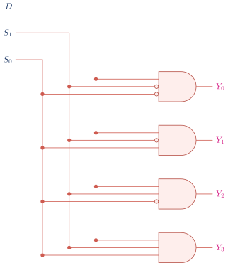
The defining behavior is that exactly one output equals the data input and the rest are forced to . Demultiplexers appear at the write side of a register file (the write-enable broadcast to exactly one of registers), at the output of a memory address decoder (the data write driven into exactly one cell), and at every place where a single source must be steered to one of several sinks under control of a select pattern.
03.Decoders and Encoders Revisited
The 2-to-4 decoder of Chapter 4 is the prototype of the decoder family. An -to- decoder takes input bits and produces outputs in which exactly one output is and the rest are . The asserted output is selected by the binary value of the input. Wider decoders appear inside every register file (the read-address decoder selects one of registers) and inside every memory array (the address decoder selects one of rows).
Hierarchical decoders
A direct 5-to-32 decoder uses thirty-two 5-input ANDs and the ten inverters that produce both polarities of the five input bits. The fan-in of each AND is and the total gate count is on the order of forty gates. A more compact alternative is to build the wider decoder hierarchically from smaller decoders. A 5-to-32 decoder can be built from one 2-to-4 decoder and four 3-to-8 decoders: the 2-to-4 decoder picks one of four groups of eight outputs by gating the enable of each 3-to-8, and each 3-to-8 selects one output within its group. The fan-in of every gate in the hierarchical version is at most rather than . The delay of the hierarchical decoder is two decoder stages rather than one, but two stages of low fan-in gates are typically faster in real cell libraries than one stage of high fan-in gates.
The trade-off generalizes. Decoder depth and fan-in are related by for an -input decoder built from -input decoder cells stacked to depth . The optimal point on the curve depends on the cell library’s fan-in versus delay characteristics. Most ASIC libraries treat or as the practical maximum, so address decoders for memories with rows are built as four stages of 4-to-16 or 5-to-32 decoders.
Decoders with enable
A decoder with enable adds a single input. When the decoder behaves normally. When every output is forced to , regardless of the address inputs. The mechanism is simple: each output AND gate receives as an additional input. The enable signal is what makes the hierarchical construction of the previous subsection work. The 2-to-4 decoder at the top of the hierarchy provides one of its four outputs as the input to each 3-to-8 decoder at the next level. Only the chosen 3-to-8 decoder is active at any time. The other three have and emit all-zeros, which is the correct behavior for a decoder whose group of eight outputs is not selected.
The enable input also serves a clocking role in some asynchronous designs and a power-saving role in others (the decoder consumes no dynamic energy when its outputs are forced to zero). The register file address decoder in Chapter 25 uses the enable input as the gate that distinguishes a read access from no-access.
Binary encoders
An encoder is the inverse of a decoder. The -to- encoder accepts input lines and produces the -bit binary index of the asserted input. The encoder assumes exactly one input line is asserted at any time. If zero or more than one input is asserted, the simple encoder’s output is meaningless.
Consider a 4-to-2 encoder with inputs and outputs . The truth table contains four valid rows, one for each pattern. Reading the binary index out of the asserted input gives the equations
The encoder is therefore an OR network. The output bit is the OR of every input whose binary index has bit set. The structure scales directly to wider encoders. A -to- encoder has output ORs, each with inputs.
The fragility of the construction is the requirement that exactly one input be asserted. Two inputs simultaneously asserted produce the OR of their indices, which is in general neither of the two input indices. A 4-to-2 encoder with outputs , which is the index of , a line that is not asserted. The priority encoder is the standard fix.
Priority encoders
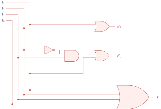
A priority encoder establishes a fixed ranking among its inputs. When multiple inputs are asserted, the encoder outputs the index of the highest-priority asserted input. A second output line called the valid signal (commonly ) is asserted when at least one input is high, allowing a downstream block to distinguish the all-zeros input pattern from a legitimate index of zero.
The standard 4-to-2 priority encoder gives highest priority to and lowest priority to . The output equations are
\begin{align} E_{1} &\;=\; I_{3} + I_{2}, \\ E_{0} &\;=\; I_{3} + \overline{I_{2}} \cdot I_{1}, \\ V &\;=\; I_{3} + I_{2} + I_{1} + I_{0}. \end{align}
Figure 2 shows the gate-level realization. The priority encoder is the natural front end of an interrupt controller, where multiple devices may request service simultaneously and the controller must select the highest-priority pending request [1][2]. The mechanism reappears in instruction scheduling (Chapter 53) where multiple ready instructions compete for issue slots and a priority encoder picks the highest- priority ready candidate.
A wider -to- priority encoder generalizes the same pattern. Each output bit is the OR of products where is an input whose binary index has bit set, and the run over all inputs strictly higher than in the priority order. The product term thus enforces the priority by blocking lower-priority inputs whenever a higher-priority input is asserted. The valid output remains the OR of all inputs. The product terms grow large for wide encoders, so practical implementations use the hierarchical leading-one detector structure that scans in steps rather than the flat OR-of-products form.
04.Comparators
A comparator reports a relationship between two multi-bit operands. The simplest variant is the equality comparator, which emits a single output bit set to when its two inputs are identical bit for bit. The magnitude comparator goes further and emits separate outputs for the three mutually exclusive relationships , , and . Both variants appear inside every CPU. The branch unit compares the contents of two registers to decide whether to take a conditional branch. The load-store queue compares addresses to detect overlapping memory accesses. The cache controller compares tag bits to decide whether a memory request hit or missed the cache.
The equality comparator
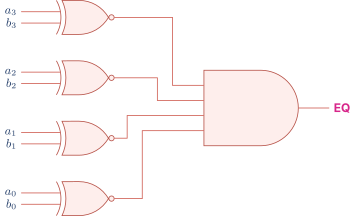
For two -bit values and , the equality output is
Each bit pair feeds an XNOR gate whose output is if and only if the two bits agree. The XNOR outputs feed one wide AND. The AND is exactly when every bit pair matches, which is the definition of equality. Figure 3 draws the structure for .
For wide operands the single wide AND becomes impractical. A 32-bit equality comparator is therefore built from eight 4-bit equality blocks whose outputs feed an 8-input AND, or from sixteen 2-bit blocks whose outputs feed a 16-input AND, or as a fully balanced tree of 2-input ANDs. The total gate count is the same either way (about XNORs plus 2-input ANDs in the balanced tree). The tree depth keeps the critical path short.
The magnitude comparator
The magnitude comparator emits the three mutually exclusive signals , , and . The recipe is a bitwise scan from the most significant bit down to the least significant. At each bit position , the comparator considers three cases. If , the relation is decided and the rest of the bits are irrelevant. If , the relation is decided. If , the decision is deferred to the next bit. The structure terminates with the equality signal when no bit position has decided the relation.
A one-bit comparator slice with inputs and inherited inputs from the bit above produces
\begin{align} \text{LT}_{i} &\;=\; \text{LT}_{i+1} + \text{EQ}_{i+1} \cdot \overline{a_{i}} \cdot b_{i}, \\ \text{GT}_{i} &\;=\; \text{GT}_{i+1} + \text{EQ}_{i+1} \cdot a_{i} \cdot \overline{b_{i}}, \\ \text{EQ}_{i} &\;=\; \text{EQ}_{i+1} \cdot \overline{a_{i} \oplus b_{i}}. \end{align}
The chain is initialized with and , meaning that before any bit has been examined the relation is tentatively equality. After processing all bits, the outputs are the final relation.
The iterative form is exactly analogous to a ripple-carry adder. Each bit’s decision feeds the next. The critical path is linear in , which limits the speed for wide operands. Parallel magnitude comparators are built by adapting the same prefix-tree ideas used for fast adders, which the next section develops in detail.
Iterative versus parallel magnitude comparison
A subtle observation makes the parallel comparator’s structure easier to see. The relations and are the same problem with the roles of and swapped. A circuit that produces the bit pattern of implicitly contains both relations: if and only if the subtraction’s result is positive and nonzero, if and only if it borrows (the sign bit of the result is under two’s-complement subtraction), and if and only if all result bits are . The magnitude comparator is therefore built into every adder/subtractor at no extra cost beyond a small bit-OR for the zero detect and the sign-bit fan-out for the negative detect. RISC-V’s SLT (set less than) and ARM’s flag-setting subtract use exactly this construction [3][4].
05.Binary Adders
The adder is the workhorse of integer arithmetic. Every instruction that increments the program counter, every offset calculation in a memory access, every signed or unsigned add instruction, and every shift-and-add multiplier turns ultimately on an -bit adder. The design space for adders is one of the richest in digital hardware. Trade-offs of area, delay, and power have been studied for sixty years, and at least a dozen distinct adder families remain in active use across modern designs. This section starts at the bit-level full-adder and works up through the four families that appear in production CPUs today.
The half-adder
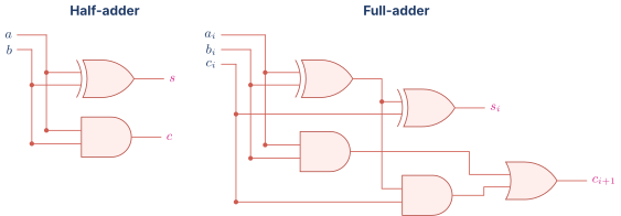
The simplest adder is the half-adder. It takes two one-bit inputs and and produces a sum bit and a carry bit . The defining equations are
The sum is the XOR of the two inputs and the carry is their AND. Implementing a half-adder takes one XOR gate and one AND gate. The half-adder is not directly useful for chaining because it has no carry-in input. The only place a half-adder appears as itself in modern CPUs is at the least significant bit of an adder when the carry-in is known to be zero, and even there a full-adder is typically substituted to keep the design regular.
The full-adder
The full-adder is the atomic unit of every chained adder. It takes three one-bit inputs and produces two outputs:
The sum is the three-way XOR of the operand bits and the incoming carry. The carry-out is asserted when at least two of the three inputs are asserted, which is the same as saying that the bit’s local generate () is asserted, or the bit’s local propagate () is asserted while a carry-in is present. Figure 4 shows both adders side by side.
The two outputs are related to a useful invariant. The numerical sum is an integer between and . The two output bits are exactly the two-bit binary representation of that integer. The full-adder thus performs a correct binary addition for the bit position, with the carry-out carrying the overflow into the next position.
The ripple-carry adder
Chaining full-adders so that the carry-out of bit becomes the carry-in of bit produces an -bit adder. The incoming carry to bit is set to for ordinary addition or to to add one (a common trick used in two’s-complement subtraction, see a later section). The chain delivers an -bit result , where is the carry-out of the most significant bit. Figure 5 draws a 4-bit ripple-carry adder.
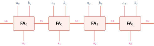
The ripple-carry adder is correct by construction and uses the smallest amount of hardware of any practical -bit adder. The single drawback is speed. The carry-out of bit cannot be computed until the carry-out of bit has settled, which in turn cannot be computed until bit has settled, and so on down to bit . The critical path through the adder traverses every full-adder in sequence. If a single full-adder’s carry-input-to-carry-output delay is , the -bit ripple-carry adder’s worst-case delay is approximately . For a 64-bit adder the linear delay is prohibitive in modern designs. The next subsections describe the three families of fast adders that break the linear scaling.
The carry-propagation bottleneck
Speeding up the adder requires breaking the chain of carry dependencies. Two observations frame the rest of the section. The first observation is that each bit position has two relevant local signals. The first, called generate, is the condition under which the bit produces a carry-out regardless of the carry-in. The second, called propagate, is the condition under which the bit passes an incoming carry through to its carry-out. For bit position , these signals are
The XOR form of matches what the full-adder already computes inside itself. Some texts use instead. Both definitions give correct carry equations because the carry-out involves as the dominant term and the distinction matters only when both and are , in which case the bit generates a carry regardless of . The XOR form has the advantage that it equals zero when the bit generates, which simplifies the prefix-tree adders introduced below. The rest of this chapter uses the XOR form.
The second observation is that the carry-out of every bit position can be expressed as a function of all the generate and propagate signals at or below it. Unrolling the recurrence from the equation above gives, for example,
\begin{align} c_{1} &\;=\; g_{0} + p_{0} c_{0}, \\ c_{2} &\;=\; g_{1} + p_{1} c_{1} \;=\; g_{1} + p_{1} g_{0} + p_{1} p_{0} c_{0}, \\ c_{3} &\;=\; g_{2} + p_{2} g_{1} + p_{2} p_{1} g_{0} + p_{2} p_{1} p_{0} c_{0}, \end{align}
and in general
The carry to position is a sum-of-products of generate and propagate signals. The critical-path delay through such a sum-of-products is independent of if the products are computed in parallel. The fan-in of the products and of the final OR grows with , however, so the scheme cannot be applied to a 64-bit adder as one flat layer. The fast adders of the next subsections are the different ways of organizing the parallel carry computation while keeping fan-in bounded.
The atomic recurrence deserves a name. It is the defining identity of every fast adder.
Every adder family below is a different way of computing the equation above for all in parallel.
The carry-lookahead adder
The carry-lookahead adder (CLA) computes the equation above directly for a fixed block size, typically four bits. A 4-bit CLA block has the four carries as outputs of a flat AND-OR network whose inputs are and the eight signals . The network has the structure
\begin{align} c_{1} &= g_{0} + p_{0} c_{0}, \\ c_{2} &= g_{1} + p_{1} g_{0} + p_{1} p_{0} c_{0}, \\ c_{3} &= g_{2} + p_{2} g_{1} + p_{2} p_{1} g_{0} + p_{2} p_{1} p_{0} c_{0}, \\ c_{4} &= g_{3} + p_{3} g_{2} + p_{3} p_{2} g_{1} + p_{3} p_{2} p_{1} g_{0} + p_{3} p_{2} p_{1} p_{0} c_{0}. \end{align}
Each is computed in parallel from the and signals of all lower bits. The longest product in the 4-bit block has five terms, which is within the fan-in budget of most cell libraries. Figure 6 draws the structure.
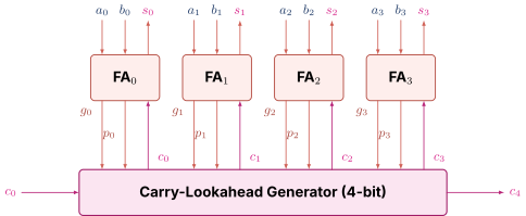
Wider adders are built from 4-bit CLA blocks chained at the block level. A 16-bit adder has four 4-bit CLA blocks. The block-level carry into block is computed by a second CLA block whose inputs are the block-level generate and propagate signals, defined as
with a similar definition for . The block-level generate is when the block produces a carry-out regardless of its carry-in, and the block-level propagate is the AND of all four bit-level propagates. A second-level CLA computes the inter-block carries from these signals. The construction extends to a hierarchy of arbitrary depth.
The total delay of a CLA built as a hierarchy of 4-bit blocks grows logarithmically in the adder width. A 64-bit hierarchical CLA has three levels: sixteen 4-bit blocks at the leaves, four second-level CLA blocks combining their signals, and one third-level CLA at the top. Each level adds about two gate delays, so the total carry latency is around six gate delays plus the final sum-bit XOR. Compared to the linear delay of the ripple-carry adder, the CLA’s delay is a qualitative speedup that made fast adders practical in the medium-scale integration era.
The carry-select adder
The carry-select adder takes a different approach to breaking the linear dependence. Rather than computing carries directly, it duplicates the higher-order ripple-carry adder once for each possible value of its carry-in (zero or one), runs both copies in parallel, and selects the correct result once the actual carry from the lower-order block arrives.
Figure 7 shows the structure for a 16-bit operand partitioned into four 4-bit blocks. The least significant 4-bit block is a normal ripple-carry adder. Each of the three higher-order 4-bit blocks is duplicated: one copy computes its sum assuming carry-in , and the other copy assuming carry-in . Both copies run concurrently with the lower ripple-carry stages. A 2-to-1 mux at the output of each duplicated block selects between the two precomputed sums when the actual carry-in arrives. The carry-out of each block is the mux selection bit for the next block.
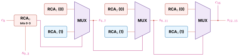
The trade-off is direct: the carry-select adder doubles the ripple hardware in every block above the LSB but cuts the worst-case delay from to with the right block size. The optimal block size grows as under the simplification that mux delay equals carry-bit delay per full-adder, which is roughly true on a typical standard-cell library. Carry-select adders are common in the upper stages of modern multipliers, where the area cost of duplication is acceptable in exchange for the latency win.
Prefix-tree adders
The prefix-tree adder family takes the most aggressive approach to parallelism. The key insight is that the carry recurrence of the equation above has the algebraic structure of an associative operator. Define the prefix operator on pairs by
This operator is associative. The carry into bit is the pair obtained by combining bits through under . The result component is when . The carry-in is folded in by combining with .
Associativity matters because it admits a parallel-prefix computation. The prefix sum of elements over an associative operator can be computed in time using a tree of operator applications, in any of several canonical structures known as parallel-prefix networks [5][6][7]. The fast adders that result are the prefix-tree adders.
Figure 8 shows the Kogge-Stone prefix tree for a 4-bit adder. The tree has levels. The first level combines adjacent pairs of bit-level generate and propagate signals. The second level combines pairs separated by two positions. The output of the tree is, at each bit position, the prefix-combined pair representing the contribution of all lower bits to that position’s carry.
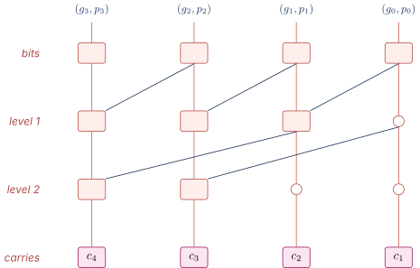
For an -bit Kogge-Stone adder, the number of levels is . The fan-in of every cell is bounded at two, which is favorable for the cell library, and the fan-out of every cell is bounded as well. The cost is the number of prefix cells: a Kogge-Stone adder uses cells, which is asymptotically . A 64-bit Kogge-Stone adder has six levels and prefix cells.
The Brent-Kung prefix tree [6] reduces the cell count to at the cost of doubling the number of levels. The tree first builds an upward sweep that combines pairs of pairs, quads of quads, and so on, then a downward sweep that distributes the combined prefixes to every position. The total cell count is , which is roughly half the Kogge-Stone count for moderate , and the level count is . The Brent-Kung adder is preferred when area matters more than absolute latency.
Two further canonical structures are common. The Han-Carlson adder is a hybrid of Kogge-Stone and Brent-Kung that runs Kogge-Stone on the odd-indexed bits and a single Brent-Kung pass on the even-indexed bits, giving an intermediate area-latency trade-off. The Sklansky adder [7] has the same logical depth as Kogge-Stone with about half the cells, but it requires much higher fan-out on internal nodes, which complicates physical implementation.
Modern industrial processors invariably use one of these four adder families for the integer ALU. Recent disclosures from Intel and AMD report Kogge-Stone variants in performance-oriented cores and Brent-Kung variants in power-oriented cores, with custom hybrids in the very widest adders inside vector units [8][1]. The proprietary details vary, but the underlying prefix structures are universally one of the four classics.
Choosing an adder for a given technology
The four adder families above span the full design space from minimum area (ripple-carry) to minimum latency (Kogge-Stone). The decision in practice depends on the operand width, the cell library’s gate delays and fan-out budget, and the timing constraints of the surrounding datapath. A few rules of thumb guide the choice. For 8-bit adders or narrower, ripple-carry is typically fast enough and unbeatable on area. For 16-bit through 64-bit adders in the integer ALU’s critical path, prefix-tree adders dominate, with Kogge-Stone in the very fastest cores and Brent-Kung or Han-Carlson in area-constrained cores. For 32-bit adders in non-critical positions (program-counter increment, memory address generation outside the load-store queue) the carry-select adder offers a good middle ground. For wide adders inside multiplier reduction trees, the operand widths shift with each reduction stage and a redundant-form representation called carry-save is used instead, as developed in Chapter 7.
The decision becomes more interesting when the surrounding datapath provides additional timing slack. A pipelined CPU can spread a wide addition across two cycles by inserting a register between two halves of the operand. The 32-bit upper-half addition can then run as a ripple-carry, since its delay budget doubled. This pipelined-add trick was the path to high-frequency operation in early superscalar designs and remains in use for the operand-forwarding paths described in Chapter 30.
06.Subtractors and Two’s-Complement Arithmetic
A circuit that adds two numbers can be repurposed to subtract them. The trick is the two’s-complement representation introduced in Chapter 3, which encodes a negative number as the bit pattern , where the addition is modulo . Substituting into gives the identity
The right-hand side is an addition of , the bitwise complement of , and the constant . The same -bit adder that computes computes if we feed it and on its operand inputs and force the carry-in to . Figure 9 shows the standard adder-subtractor unit. A single mode bit selects between addition () and subtraction (). The mode bit XORs into every bit of operand on the way to the adder, which inverts the operand bits when and leaves them unchanged when . The same mode bit feeds the carry-in of the adder, producing the trailing when .
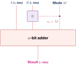
The adder-subtractor unit is what every CPU ALU contains. RISC-V’s ADD and SUB instructions are implemented by exactly this circuit, with the funct7 bit of the instruction encoding mapped directly to the mode bit [3]. ARM’s ADD and SUB likewise share the unit, with the additional complication of an optional shift on operand before it enters the XOR bank [4]. Intel x86-64 ADD and SUB share the same arithmetic core inside the integer execution unit, with additional flag-generation logic that the RISC-V and ARM cores do not produce.
Carry, borrow, and overflow
The adder-subtractor produces two pieces of side-channel information beyond the sum bits themselves. The carry-out of the most significant bit and the overflow flag have distinct interpretations under the two operand encodings.
Under unsigned arithmetic, the carry-out of the most significant bit is set when the true mathematical sum exceeds . For an -bit addition this means the result wrapped around modulo . For a two’s-complement subtraction implemented as , the carry-out reads as a borrow signal inverted. The carry-out is when no borrow was required (the unsigned result was nonnegative) and when a borrow was required. Architecturally, x86-64 inverts the carry-out on subtraction so that the carry flag has the natural borrow semantics. RISC-V does not have a carry flag at all and emits the same hardware signal under the alternative name when the programmer needs it.
Under signed (two’s-complement) arithmetic, the carry-out of the most significant bit does not directly indicate overflow. Signed overflow occurs when the result of a signed addition or subtraction cannot be represented in bits as a two’s-complement integer. The detection rule was developed in Chapter 3: signed overflow occurs when the operand signs are the same and the result sign is different (for addition), or when the operand signs are different and the result sign differs from the sign of the minuend (for subtraction). The standard circuit-level test is
where is the carry-out of the most significant bit and is the carry-out of the second most significant bit. The two carries match when no overflow has occurred and differ when overflow has occurred. The XOR of the two top carries is therefore exactly the signed-overflow flag. Most ALUs route both top carries out of the adder to a small overflow-detection block that produces for the flag register.
Decimal subtraction in passing
The two’s-complement trick also has a binary-coded-decimal (BCD) analog. A decimal subtractor exists in some legacy CPUs (most visibly x86’s AAS and DAS instructions, which are decoded but no longer perform their original function on recent x86-64 microarchitectures) and operates by precomputing the nine’s-complement of the subtrahend digit and adding it with a carry-in of one to the minuend. The decimal nine’s-complement plus one is the decimal analog of the binary two’s-complement. The BCD adder/subtractor has additional correction logic when a digit-sum exceeds nine, but the overall pattern of "complement and add" is identical to the binary case. The decimal arithmetic unit is rare in modern CPUs and is included here only as acknowledgment that the two’s-complement subtraction trick is not specific to binary.
07.Shifters
A shifter takes an -bit input and produces an -bit output whose bits are the input bits shifted left or right by a specified amount. Shifters appear inside the integer ALU as direct support for the shift instructions in every modern ISA. They also appear inside multipliers (as part of the shift-and-add construction) and inside floating-point units (to align operands before addition).
Fixed shifts and arithmetic shifts
The simplest shifter shifts by a fixed amount known at synthesis time. A 1-bit left shifter takes an input and produces . The output is a permutation of the input wires plus a constant zero filling the vacated bit. A fixed shifter consumes no logic gates at all: it is implemented as a permutation of wires, which is free in cost terms (silicon area is consumed only by the wiring itself, not by any logic cell).
A fixed right shifter introduces a complication. Logical right shift fills the vacated bits at the high end with zeros. Arithmetic right shift fills them with copies of the most significant input bit (the sign bit). The two operations differ only in the high- end fill pattern, but the difference is essential under two’s-complement: arithmetic right shift preserves the sign of a negative number, while logical right shift treats the number as unsigned. RISC-V exposes both via SRL (logical) and SRA (arithmetic), and the same distinction exists in every other major ISA [3][4][9].
The barrel shifter
A barrel shifter accepts a variable shift amount as an input operand. The output is the input shifted by the requested amount in a single pass. The standard structure is a logarithmic tree of multiplexer stages. Each stage shifts conditionally by a power of two: the first stage shifts by or , the second stage by or , the third stage by or , and so on. A shifter that handles all shift amounts from to has stages. Figure 10 draws a 4-bit left barrel shifter with two stages.
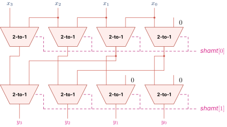
The total mux count is , and the critical-path delay is mux delays. A 32-bit barrel shifter has 160 muxes and a five-stage delay. The barrel structure is the canonical implementation in every modern ISA’s shift unit. Some ISAs reuse the same shifter for both left and right shifts by gating the routing direction with a one-bit control input, and some provide separate left and right shifter units. The trade-off is a small amount of additional control logic against the unit duplication.
The barrel shifter also handles arithmetic right shifts. The fill bits at the high end are gated by the sign bit of the input operand. A single AND gate per mux input on the rightmost path of each stage suffices. Most cell-library implementations include sign-extension as part of the shifter cell rather than as a separate stage.
Rotation operations
A rotation is a shift that wraps the bits shifted out of one end back into the other. A 1-bit left rotation of is . The barrel-shifter structure of the previous subsection supports rotation with one minor change. The bits shifted in from one end are the bits shifted out from the other end, rather than zeros. Each mux’s second-input source is therefore the bit at position rather than zero. The hardware is the same shape, and only the routing is different.
Rotation appears in cryptographic primitives (the AES round transformation, SHA-256 round constants, many block-cipher substitution boxes), in bit-manipulation extensions, and in some hash-function inner loops where a fast bit rotation is essential. RISC-V’s Zbb provides ROL and ROR. ARMv8 provides ROR via the immediate-shift form of arithmetic instructions. x86-64 provides ROL, ROR, RCL and RCR.
Funnel shifters
A funnel shifter takes a -bit concatenation of two -bit inputs and produces an -bit window extracted at a variable offset. The structure is a generalization of the barrel shifter in which the "fill" bits are not zero but the second input operand’s bits. Two operations make the funnel shifter visible to the programmer.
The x86-64 SHRD (shift right double) and SHLD (shift left double) instructions implement funnel shifts directly. SHRD dst, src, count extracts the -bit window from the -bit concatenation src | dst shifted right by count bits and stores the result in dst [9]. The ARMv8 EXTR instruction performs the same operation under a slightly different syntax [4].
The microarchitectural implementation is a single barrel shifter operating on the -bit concatenation, with the output taken from a fixed window. The shift unit’s silicon cost is roughly twice that of an -bit barrel shifter, but it provides the fast funnel-shift operation that arbitrary-precision arithmetic and string-search inner loops depend on.
08.Putting It Together: A Sketch of a Simple ALU
The blocks of this chapter combine into an arithmetic logic unit (ALU), the workhorse functional unit of every general-purpose CPU. The ALU takes two operand inputs and a function code, performs the selected arithmetic or logical operation, and produces a single result output together with a set of side-channel flags. The simple ALU developed below supports eight functions: add, subtract, AND, OR, XOR, NOR, set- less-than, and barrel-shift-left. The function code is a 3-bit input that selects among the eight.
Function selection through a mux
The ALU computes the results of all eight functions and selects one with an 8-to-1 multiplexer. Seven functional units supply those results in parallel, because the shared adder/subtractor emits either or according to its mode bit rather than both at once. The candidate results are
-
(add) and (sub), both from the adder/subtractor unit of a later section.
-
(bitwise AND), in the Boolean sense (bitwise OR), (bitwise XOR), and (bitwise NOR), all produced by a parallel bank of corresponding 2-input logic gates.
-
Set-less-than: a 1-bit signal asserted when under signed comparison, packaged as an -bit value whose low bit is the signal and whose upper bits are zero. The signal comes from the sign bit of the subtraction XORed with the overflow flag, which gives a correct signed less-than for the two’s-complement encoding.
-
(logical left shift by the low bits of ), produced by a barrel shifter.
Figure 11 shows the block-level structure.
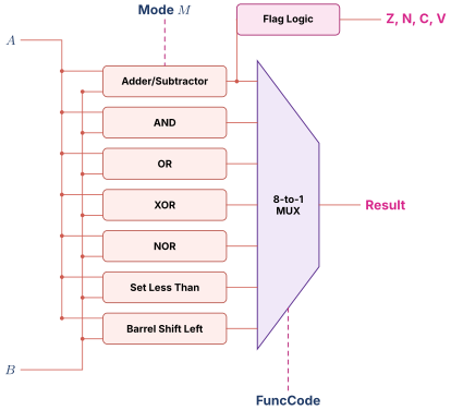
The structure shown is the eager-execution form: every functional unit runs on every cycle and the mux at the end selects which result reaches the output. The unselected units still consume dynamic power as they switch. A low-power alternative is the lazy-execution form, in which a decoder upstream of the functional units selectively enables only the unit corresponding to the function code. The latter form is more energy-efficient but adds one decoder-stage delay to the critical path. Modern CPUs use both forms in different parts of the datapath. The integer ALU in a high-frequency core is typically eager. The integer ALU in a low-power core is typically lazy. The trade-off is the same area-versus-power trade-off that recurs throughout digital design.
Flag generation
The flag-logic block at the top of Figure 11 produces four single-bit outputs that downstream blocks use to make decisions. The Zero flag is asserted when every bit of the ALU result is . The Negative flag is the most significant bit of the ALU result, which under two’s-complement is the sign of the integer. The Carry flag is the carry-out of the adder’s most significant bit (or its inverse under subtraction, depending on the ISA’s convention). The oVerflow flag is the XOR of the top two carries from the adder, the equation above.
The exact set of flags differs across ISAs. x86-64 carries a six-flag register (Carry, Parity, Auxiliary Carry, Zero, Sign, Overflow), ARMv8 carries the four flags above under the names N, Z, C, V, and RISC-V carries no flag register at all and instead expects the programmer or compiler to materialize the equivalent information via explicit compare instructions when needed [9][4][3]. The underlying ALU hardware is structurally similar. The variation is in which side-channel signals are exposed at the architectural level.
What the simple ALU does not include
The ALU sketched above is deliberately minimal. Three substantial omissions are worth noting.
Multiplication is not present. A combinational -bit multiplier is significantly larger than an adder and is the main subject of Chapter 7. Most CPUs implement multiplication as a multi-cycle sequential block that uses a much smaller hardware footprint than a full combinational multiplier. The sequential multiplier consumes an adder of the type developed in this chapter plus a small shift register and a control state machine.
Division is also not present. Division is even more expensive than multiplication and is invariably implemented as a multi- cycle iterative algorithm. Restoring division, non-restoring division, SRT division, and Newton-Raphson division are the four families that production CPUs use, all developed in Chapter 7.
Floating-point operations are not present in this ALU. They live in a separate functional unit, the floating-point unit (FPU), which has its own adder, multiplier, and shifter sized for the IEEE 754 representation. The FPU is the topic of Chapter 8.
09.Looking Ahead
The combinational vocabulary of this chapter is complete enough to express almost every datapath operation in a CPU. Adders feed the program counter and the load-store address generator. Subtractors and comparators implement conditional branches. Multiplexers route data between register file, ALU output, and memory read. Decoders enable register-file writes and memory-row selection. Encoders and priority encoders pick the highest- priority ready instruction in an issue queue. Shifters implement the explicit shift instructions and the implicit shifts inside multiplication and floating-point alignment.
What is still missing is time. Every block of this chapter is combinational, meaning its outputs settle to a fixed function of its inputs after a propagation delay and then sit there until the inputs change again. A working processor needs storage that holds a value across cycles, edges that synchronize updates, and a clock distribution network that keeps every storage element ticking together. Chapter 6 introduces those elements. Chapter 7 returns to arithmetic to develop multiplication and division. Chapter 25 combines the combinational blocks of the present chapter with the sequential storage of Chapter 6 into the first complete CPU datapath in the book.
10.Worked Examples
11.Exercises
References
- [1]Harris, Sarah L. and Harris, David Money (2021). “Digital Design and Computer Architecture.” Morgan Kaufmann.
- [2]Patterson, David A. and Hennessy, John L. (2020). “Computer Organization and Design RISC-V Edition: The Hardware Software Interface.” Morgan Kaufmann.
- [3]Waterman, Andrew and Asanovi\'c (2024). “The RISC-V.”
- [4](2024). “ARM.”
- [5]Kogge, Peter M. and Stone, Harold S. (1973). “A Parallel Algorithm for the Efficient Solution of a General Class of Recurrence Equations.” IEEE Transactions on Computers, C-22(8), pp. 786--793. doi:10.1109/TC.1973.5009159
- [6]Brent, Richard P. and Kung, H. T. (1982). “A Regular Layout for Parallel Adders.” IEEE Transactions on Computers, C-31(3), pp. 260--264. doi:10.1109/TC.1982.1675982
- [7]Sklansky, Jack (1960). “Conditional-Sum Addition Logic.” IRE Transactions on Electronic Computers, EC-9(2), pp. 226--231. doi:10.1109/TEC.1960.5219822
- [8]Hennessy, John L. and Patterson, David A. (2019). “Computer Architecture: A Quantitative Approach.” Morgan Kaufmann.
- [9](2024). “Intel.”