ARM A64: The Mobile and Server Workhorse
September 8, 202640 min readintermediate
ARM processors power nearly every smartphone on the planet, a growing share of laptops and desktops (the Apple M series, Qualcomm Snapdragon X), and an expanding footprint in servers and supercomputers (AWS…
ARM processors power nearly every smartphone on the planet, a growing share of laptops and desktops (the Apple M series, Qualcomm Snapdragon X), and an expanding footprint in servers and supercomputers (AWS Graviton, Ampere Altra, Fujitsu A64FX in the former #1-ranked Fugaku). The ARM ecosystem ships more processors per year than any other ISA family. The 64-bit instruction set, A64, introduced with ARMv8-A in 2011, was a clean-slate redesign that broke encoding compatibility with the earlier 32-bit A32 and Thumb encodings while preserving toolchain continuity and a shared architectural philosophy.
This chapter examines the A64 instruction set in detail. It covers the register file, the instruction encoding groups, the exception-level hierarchy, the NEON and SVE/SVE2 vector extensions, and the evolution from ARMv8-A through ARMv9-A. The presentation assumes the vocabulary of Chapter 13 and the RISC/CISC classification framework of Chapter 14. Where comparisons with RISC-V illuminate a design choice, the chapter draws them explicitly [1].
01.The AArch64 Register File
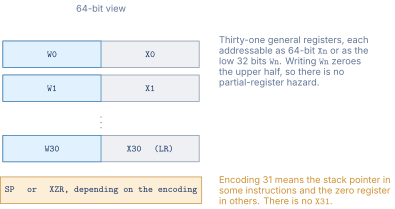
Figure 1 shows the file and its one irregularity.
General-purpose registers
AArch64 provides 31 general-purpose registers, X0 through X30, each 64 bits wide. Every register has a 32-bit alias: W0 through W30. An instruction that writes to a W register zeros the upper 32 bits of the corresponding X register. This zero-extension rule eliminates the partial-register stalls that plagued the x86 architecture when a write to EAX left the upper 32 bits of RAX unchanged.
Register X30 serves as the link register (LR). The BL (branch with link) instruction writes the return address to X30 before branching. A function returns by executing RET, which branches to the address in X30 (or another register, if specified).
The zero register and the stack pointer
A64 does not dedicate a register number to the zero register the way RISC-V dedicates x0. Instead, the encoding that would refer to a 32nd register (register number 31) is interpreted differently depending on the instruction. Some instructions interpret register 31 as the zero register XZR/WZR, which always reads as zero and discards writes. Other instructions interpret register 31 as the stack pointer SP. The distinction is documented per instruction in the ARM Architecture Reference Manual [1]. The dual interpretation is a clever encoding trick that saves an opcode bit at the cost of a small lookup table in the decoder.
The program counter
The program counter is not a general-purpose register in AArch64. It cannot be named as a source or destination in data-processing instructions. It is accessible only through PC-relative addressing (the ADR and ADRP instructions) and through branch instructions. This restriction simplifies the pipeline because the program counter does not compete for read or write ports on the integer register file.
PSTATE and condition flags
The PSTATE register holds the four condition flags (N, Z, C, V), the current exception level, the stack pointer select bit (which chooses between SP_EL0 and SP_ELn at each exception level), the DAIF interrupt mask bits (Debug, SError, IRQ, FIQ), and several other control fields. The condition flags are updated only by instructions that explicitly request it (those ending in S, such as ADDS and SUBS, along with aliases built on them such as CMP, which is SUBS with XZR as the destination). This selective update, discussed in Chapter 13, reduces false dependencies in the out-of-order engine.
Floating-point and SIMD registers
A64 provides 32 registers, V0 through V31, each 128 bits wide. These registers serve triple duty: as scalar floating-point registers (accessed as D0–D31 for 64-bit doubles, S0–S31 for 32-bit floats, H0–H31 for 16-bit half-precision), as NEON SIMD registers (accessed as 128-bit V registers holding lanes of 8, 16, 32, or 64-bit elements), and as SVE vector registers (where the implementation may extend them beyond 128 bits). The register sharing means that a function that uses scalar double-precision arithmetic and a function that uses NEON vectors compete for the same 32-entry register file.
02.Instruction Encoding
Every A64 instruction is exactly 32 bits, fetched and decoded as an aligned 4-byte word. The encoding is fixed-width, like RISC-V, and for the same reasons: simplified fetch, trivial instruction- boundary detection, and easy multi-issue slicing.
Major encoding groups
The top 4 bits of the instruction word (bits [31:28], together with bits [27:25]) divide the encoding space into several major groups:
-
Data processing (immediate): arithmetic and logical operations with an immediate operand. Includes
ADD,SUB,AND,ORR,MOV,MOVZ,MOVK. -
Data processing (register): arithmetic, logical, and shift operations with register operands. Includes
ADD,SUB,AND,LSL,MADD(multiply-add). -
Loads and stores: all memory-access instructions, including base-plus-offset, pre-index, post-index, register offset, literal (PC-relative), and load/store pair.
-
Branches: conditional branches (
B.cond), unconditional branches (B,BL), compare-and- branch (CBZ,CBNZ), test-and-branch (TBZ,TBNZ), and system instructions (SVC,MSR,MRS). -
SIMD and floating-point: scalar FP operations, NEON vector operations, and (when present) SVE/SVE2 instructions.
The encoding compared with RISC-V
Both A64 and RISC-V use 32-bit fixed-width encodings, but the internal organization differs. RISC-V uses a 7-bit opcode at a fixed position with subsidiary function fields. A64 uses a hierarchical bit-field scheme in which the top bits select the group and subsequent bits select the specific instruction within the group. RISC-V places register specifiers at the same bit positions across all formats. A64 places them at consistent but not identical positions (the destination register is always at bits [4:0], the first source at bits [9:5], the second source at bits [20:16] for most instructions). Both designs prioritize early register extraction, allowing the rename stage to start before full decode completes.
03.Data Processing Instructions
Arithmetic instructions
The base arithmetic instructions (ADD, SUB, ADC, SBC) operate on 32-bit or 64-bit register values. The operand size is selected by the sf bit (bit 31): when sf = 0, the instruction operates on W registers (32-bit), and when sf = 1, on X registers (64-bit). Each instruction has a flag-setting variant (ADDS, SUBS) that updates the NZCV condition flags. The non-flag-setting variant leaves the flags unchanged.
Logical instructions
AND, ORR, EOR (exclusive OR), and ORN (OR NOT) operate on register pairs. The immediate forms of logical instructions use a bitmask immediate encoding that can represent a remarkably wide range of repeating bit patterns in a compact 13-bit field. The encoding covers all values of the form “ consecutive ones, rotated by positions, replicated to fill the register width,” where and are parameterized by the 13 bits. This lets common constants like 0xFF, 0xFFFF, 0x5555555555555555, and mask values for bitfield extraction fit in a single instruction.
Multiply and divide
A64 includes integer multiply (MUL), multiply- accumulate (MADD, MSUB), and widening multiply (SMULL, UMULL) as base instructions, not as an extension. The fused multiply-add is particularly useful for address calculation (base + index * stride) and for polynomial evaluation, reducing a two-instruction sequence to one. Integer divide (SDIV, UDIV) is also in the base.
The inclusion of multiply and divide in the base A64 instruction set contrasts with RISC-V, where those operations live in the separate M extension. ARM’s reasoning is pragmatic: by 2011, when ARMv8-A was designed, transistor budgets were large enough that a hardware multiplier and divider added negligible area to an application processor core, and leaving them out would force every compiler and operating system to include software fallback routines. RISC-V’s reasoning is different: the modular extension model lets a minimal microcontroller (targeting cost and area) omit the multiplier entirely, while an application processor includes it by implementing the M extension. Both approaches are valid for their target markets.
Bitfield and extract instructions
A64 provides a rich set of bitfield manipulation instructions. BFM (bitfield move) copies a contiguous field of bits from one register into a specified position in another. UBFX (unsigned bitfield extract) extracts a field and zero-extends it. SBFX (signed bitfield extract) extracts and sign-extends. BFI (bitfield insert) inserts a field into a register without disturbing the other bits. These instructions replace multi-instruction shift-and-mask sequences and are heavily used by compilers for struct field access, bit-packed data formats, and protocol header parsing.
Conditional select and conditional compare
Instead of conditional execution of arbitrary instructions (a feature of the earlier A32 encoding that predicated almost every instruction on a condition code), A64 provides a set of conditional select instructions. CSEL Xd, Xn, Xm, cond writes Xn to Xd if the condition is true, or Xm if false. Variants include CSINC (conditional select and increment), CSINV (conditional select and invert), and CSNEG (conditional select and negate). These instructions let the compiler convert short if-then-else sequences into straight-line code without branches, avoiding branch-prediction penalties for unpredictable branches.
CCMP and CCMN (conditional compare) allow chaining multiple conditions without branches. CCMP compares two registers and updates the condition flags only if a prior condition holds. If the prior condition does not hold, the flags are set to an immediate value specified in the instruction. This mechanism allows expressions like “if (a > 0 && b < 10 && c == 5)” to be evaluated without any branches.
Why A64 threw away full predication
The sentence that opens this subsection contains one of the most interesting decisions in A64, and it is easy to read past. ARM had full predication in A32, where nearly every instruction carried a 4-bit condition field and executed only if the flags matched. It was a signature feature, widely admired, and taught as one of the things ARM got right. A64 removed it and kept only a handful of conditional select instructions. Understanding why is worth more than memorizing the replacement.
Full predication was designed for a short, in-order pipeline. On such a machine a mispredicted branch costs three or four cycles, and a predicated instruction that turns out not to execute costs one cycle: it flows through the pipeline and its write is suppressed at the end. Trading branches for predication is obviously profitable at those numbers.
Three things changed.
Pipelines got deeper and predictors got better. A modern branch predictor is correct on well over 95 percent of dynamic branches. Predication pays a guaranteed cost on every instruction it covers, while a predicted branch pays nothing on the overwhelming majority of executions and a large penalty rarely. Once the predictor is good, the guaranteed cost is the worse deal for any branch that is predictable at all.
Predication is expensive under register renaming. This is the decisive one and it is not obvious. A predicated ADD R0, R1, R2 does not always write R0, so the renamer cannot simply allocate a new physical register and record that it holds R0. It must produce a value that is either the sum or the old R0, which means the instruction has a third source operand: its own destination. Every predicated instruction therefore reads one more register than it appears to, and the dependence on the old value is real, so it constrains scheduling even when the condition is false.
The encoding cost was paid by every instruction. Four bits of every 32 were spent on a condition field that, in practice, carried AL (always) in the large majority of instructions. A64 reclaimed those bits and spent them on wider immediates, a larger register file specifier and more opcode space.
Figure 2 contrasts the two approaches on the same conditional assignment.
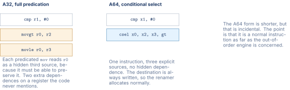
CSEL keeps the benefit and drops the cost. It always writes its destination, so it renames like any other instruction. It names all three of its inputs explicitly, so there is no hidden dependence. And it exists in exactly the case predication was good at, the short unpredictable if-then-else, while leaving longer or predictable regions to the branch predictor.
04.Loads, Stores, and Addressing Modes
A64 provides a richer set of addressing modes than RISC-V, though fewer than x86-64.
Base plus immediate offset
The most common form. LDR X1, [X0, #16] loads a 64-bit value from address X0 + 16. The immediate is unsigned and scaled by the access size (so for a 64-bit load, the 12-bit immediate is multiplied by 8, giving a range of 0 to 32,760 bytes in steps of 8).
Pre-index and post-index
LDR X1, [X0, #16]! (pre-index) first adds 16 to X0, then loads from the updated address. LDR X1, [X0], #16 (post-index) loads from the current X0, then adds 16 to X0. Both modes use a signed 9-bit immediate (range to bytes, unscaled).
Register offset
LDR X1, [X0, X2] loads from address X0 + X2. An optional shift or extend modifier can scale the index: LDR X1, [X0, X2, LSL #3] loads from X0 + X2 * 8. This mode covers the same use case as x86-64’s SIB byte and is the closest A64 equivalent to scaled- index addressing.
PC-relative literal
LDR X1, label loads a value from a PC-relative address. The offset is a 19-bit signed value scaled by 4, giving a range of MiB. The ADRP instruction forms a 4 KiB- aligned page address: it shifts a 21-bit signed immediate left by 12 and adds it to the current page-aligned PC. Paired with a subsequent LDR that adds the page offset, ADRP reaches any address within GiB of the current PC, which is sufficient for position-independent code.
Load and store pair
LDP X1, X2, [X0] loads two consecutive 64-bit values in a single instruction: X1 from [X0] and X2 from [X0 + 8]. The corresponding STP stores two values. Pair instructions are heavily used in function prologues and epilogues to save and restore callee- saved registers two at a time, cutting the number of memory instructions in half.
Why a pair instruction earns its encoding space
Cutting the number of instructions in half is the obvious benefit and it is the smaller one. LDP and STP exist because of what they do to the memory system, not to the instruction count.
A 64-bit store sends eight bytes to the store buffer. Two of them send eight bytes twice, occupying two store-buffer entries and two cycles of the store port. STP of an adjacent pair sends sixteen bytes as a single access, taking one entry and one cycle, because the two halves fall in the same aligned sixteen-byte block and the hardware can merge them at issue rather than hoping the store buffer coalesces them later. The store port, not the instruction stream, is the resource being conserved.
That matters because of where these instructions actually appear. A function prologue that saves the frame pointer, the link register and four callee-saved registers is six stores, and it runs on entry to every non-leaf function in the program. The epilogue is six loads. Function call overhead is one of the most-executed patterns in any program, and halving both its instruction count and its memory-port occupancy is worth a great deal more than the same saving applied to arithmetic.
The standard AArch64 prologue makes the intent visible:
| stp x29, x30, [sp, #-48]! ; save FP and LR, pre-decrement SP | |
| mov x29, sp ; establish frame pointer | |
| stp x19, x20, [sp, #16] ; save two callee-saved registers | |
| stp x21, x22, [sp, #32] ; and two more | |
| ... | |
| ldp x21, x22, [sp, #32] | |
| ldp x19, x20, [sp, #16] | |
| ldp x29, x30, [sp], #48 ; restore, post-increment SP | |
| ret |
Note that the first STP also performs the stack adjustment through the pre-index writeback, and the last LDP undoes it through post-index. Allocating the frame, saving the frame pointer and saving the return address are three conceptual operations in one instruction, and the same holds in reverse on the way out. A six-instruction prologue on a load-store ISA without pairs or writeback would be eleven.
This is also a clean illustration of a point from Chapter 14: LDP with writeback is exactly the kind of composite operation the strict RISC position argues against, and ARM included it because the pattern it serves is executed constantly and its components are always adjacent. RISC-V made the opposite call and has no pair instruction, which is a visible part of why RISC-V prologues are longer.
05.Exception Levels
AArch64 defines four exception levels, numbered EL0 through EL3. The numbering reflects increasing privilege: EL0 is the least privileged and EL3 is the most privileged.
EL0 runs user applications. Code at EL0 cannot access most system registers, cannot modify the page tables, and cannot disable interrupts.
EL1 runs the operating system kernel. It manages virtual memory through the page tables, handles exceptions and interrupts, and controls the system registers that govern memory attributes, cache maintenance, and TLB management.
EL2 runs a hypervisor. It manages the stage-2 page tables that virtualize memory for guest operating systems running at EL1. ARM’s Virtualization Host Extensions (VHE), introduced in ARMv8.1-A, allow the hypervisor to use EL2 as if it were EL1, reducing the overhead of hosting a single guest OS (the common case for container-based cloud workloads).
EL3 runs the secure monitor. It controls transitions between the Secure and Non-secure security states. The Secure state has its own EL0 and EL1 (and optionally EL2) that run trusted firmware and trusted applications. The secure monitor at EL3 arbitrates between the two worlds.
When an exception occurs (a synchronous fault, an IRQ, an FIQ, or a system error), the processor saves the return address in ELR_ELn, saves the processor state in SPSR_ELn, records the exception cause in ESR_ELn, and branches to the appropriate entry in the vector table whose base is stored in VBAR_ELn. The vector table has 16 entries, organized as four groups of four. Each group corresponds to one source state (current EL with SP_EL0, current EL with SP_ELn, lower EL in AArch64, lower EL in AArch32), and within a group the four entries are the synchronous exception, IRQ, FIQ, and SError handlers in that order.
Table 1. ARM AArch64 exception levels and their typical occupants.
| Level | Privilege | Typical occupant |
|---|---|---|
| EL0 | Lowest | User applications |
| EL1 | OS | Operating system kernel (Linux, Windows, macOS) |
| EL2 | Hypervisor | Virtual machine monitor (KVM, Xen, Hyper-V) |
| EL3 | Highest | Secure monitor firmware (ARM Trusted Firmware) |
Exception levels and security states are two axes, not one
The table above presents privilege as a single ladder, which is how exception levels are usually introduced and is not the whole structure. AArch64 has a second, independent axis: the security state, which is either Secure or Non-secure. A processor is always at some exception level and in some security state, and the two are separate.
This is the part that reliably confuses people on first contact, because the obvious mental model, that Secure means more privileged, is wrong. A Non-secure EL1 kernel and a Secure EL1 kernel are at the same privilege level as each other. What differs is which physical memory and which peripherals they can reach. Secure EL1 can see memory that Non-secure EL1 cannot see at all, and the partition is enforced in the interconnect rather than by the page tables.
Figure 3 draws the grid.
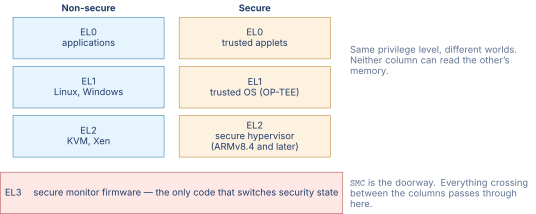
EL3 is drawn spanning both columns because it is the only code that exists outside the distinction. Its purpose is to save the state of one world, restore the state of the other, and return, and the instruction that reaches it is SMC, the secure monitor call. That is the mechanism behind a great deal of what a phone does invisibly: verifying a fingerprint without the kernel seeing the template, decrypting protected video without the kernel seeing the keys, and holding the device’s root keys somewhere a compromised kernel cannot reach.
06.NEON (Advanced SIMD)
NEON is ARM’s original SIMD extension, mandatory in all AArch64 implementations. It operates on the 32 V registers, each 128 bits wide. A NEON instruction treats a V register as a vector of lanes: 16 lanes of 8-bit integers, 8 lanes of 16-bit integers, 4 lanes of 32-bit integers or single-precision floats, or 2 lanes of 64-bit integers or double-precision floats.
NEON provides arithmetic (add, subtract, multiply, multiply- accumulate, absolute difference), logical (AND, OR, XOR, NOT), shift (left, right logical, right arithmetic), comparison (greater than, equal, less than, producing a mask), table lookup, permutation (zip, unzip, transpose), and type-conversion instructions across all lane widths. A single FADD V0.4S, V1.4S, V2.4S instruction adds four pairs of single- precision floats in one operation.
NEON’s fixed 128-bit width means that code compiled with NEON instructions is tied to 128-bit hardware. Unlike SVE, there is no length-agnostic mechanism. A processor that wants wider vectors must use SVE. This distinction parallels the relationship between x86-64’s SSE (128-bit fixed) and AVX (256-bit fixed) extensions, both of which are superseded in concept by ARM’s scalable approach.
NEON includes several instructions that have no direct equivalent in the scalar ISA. The TBL (table lookup) instruction uses a vector of byte indices to gather elements from one to four source registers, which is useful for byte-level permutations in cryptographic algorithms and image processing. The ZIP, UZP, and TRN (transpose) instructions interleave, deinterleave, and transpose vector elements, supporting the data layout transformations that matrix and signal- processing algorithms require. The SADDLP and UADDLP (pairwise add long) instructions add adjacent pairs of elements and widen the result, which is useful for horizontal reductions that accumulate a vector into a scalar.
07.SVE and SVE2: Scalable Vectors
The Scalable Vector Extension (SVE), introduced with ARMv8.2-A, takes the same length-agnostic approach as the RISC-V V extension. SVE vector registers, Z0 through Z31, extend the lower 128 bits of the NEON V registers to an implementation-defined width that can be any multiple of 128 bits from 128 up to 2048 bits, giving sixteen possible lengths. The same binary runs on all of these widths. The hardware sets a register called the Vector Length (VL), and the CNTB/CNTH/ CNTW/CNTD instructions let software query the number of active elements at run time.
SVE introduces 16 predicate registers (P0 through P15), each containing one bit per byte of vector length. Predicate registers control which lanes of a vector operation are active. A loop that processes 1000 elements on a processor with 256-bit vectors (4 double-precision lanes) runs through 250 iterations, with each iteration processing 4 elements. The same loop on a processor with 512-bit vectors (8 lanes) runs through 125 iterations. The loop does not need recompilation because the predicate-driven loop-tail handling adjusts automatically.
SVE2, mandatory in ARMv9-A, extends SVE with instructions for fixed-point arithmetic, polynomial multiplication, bit permutations, and cryptographic operations. SVE2 is designed to be a complete replacement for NEON in the scalable-vector framework. New code targeting ARMv9-A and later can use SVE2 for all SIMD work and ignore the fixed-width NEON encoding entirely.
Predicates versus a vector-length register
SVE and RISC-V’s V extension solve the same problem and do not solve it the same way, and the difference is worth drawing out because it is the clearest case in this part of the book of two competent teams reaching different answers from the same starting point.
RISC-V puts the active element count in a register. VSETVLI writes vl, every vector instruction operates on the first vl elements, and a short final iteration is expressed by vl being smaller. It is one number, and it applies to everything.
SVE puts the active elements in a mask. Sixteen predicate registers p0–p15 hold one bit per element, instructions carry a predicate operand, and an element is processed if its bit is set. The loop-control instruction WHILELT generates the predicate directly from a loop counter and a bound, setting exactly the bits for elements still within range.
Figure 4 puts both on the same ten-element loop.
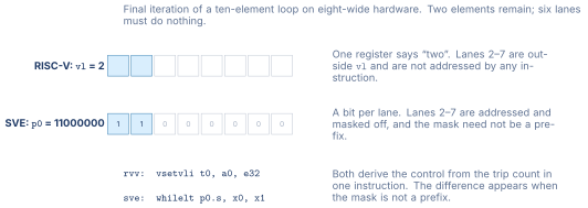
For the loop-remainder case the two are interchangeable, and both achieve the goal that made them worth building: one binary, any vector width, no cleanup loop. The divergence is elsewhere.
A predicate can express an arbitrary subset of lanes. A vector length can express only a prefix. That matters for conditional code inside a vectorized loop, the pattern if (x[i] > 0) y[i] = f(x[i]), where the active lanes are whichever ones satisfied the test and are scattered through the register. SVE handles this by computing a predicate from a comparison and using it directly. RISC-V handles it too, through mask registers that the V extension also provides, so the real distinction is emphasis rather than capability: SVE made masking the primary mechanism and derives loop control from it, while RISC-V made loop control primary and provides masking alongside.
The cost of SVE’s choice is register state. Sixteen predicate registers must be saved and restored on a context switch, and they are part of the signal-handling and thread-switch cost of every SVE process. The cost of the RISC-V choice is that vl is a mode: it persists across instructions, so a function that changes it must restore it, and the interaction with calls is a real source of ABI complexity.
08.The ARMv8 to ARMv9 Evolution
The ARM architecture evolves through point releases that add features without breaking backward compatibility. ARMv8-A was the original 64-bit specification (2011). Subsequent releases added capabilities:
ARMv8.1-A (2014): large system extensions (LSE) for atomic operations (compare-and-swap, atomic add, atomic bit set/ clear), replacing the load-exclusive/store-exclusive pair for common synchronization patterns. VHE for efficient hypervisor hosting.
ARMv8.2-A (2016): SVE for scalable vectors. Half- precision floating-point extensions (FP16). Statistical profiling extension (SPE) for hardware-assisted performance sampling.
ARMv8.4-A (2017): nested virtualization, secure EL2, and MPAM (Memory Partitioning and Monitoring) for cache and memory bandwidth partitioning in cloud environments.
ARMv8.5-A (2018): memory tagging extension (MTE), which tags each 16-byte granule of physical memory with a 4-bit color and checks the tag on every load and store. If the pointer’s tag does not match the memory’s tag, the processor raises a fault. MTE is a hardware mechanism for detecting use-after-free and buffer-overflow bugs, two of the most common security vulnerabilities in C and C++ programs. Branch target identification (BTI) for forward-edge control-flow integrity was also introduced here.
ARMv8.6-A (2019): bfloat16 (BF16) extensions for machine-learning inference, enhanced counter virtualization for cloud workloads, and fine-grained traps for virtualization.
ARMv9-A (2021): a major branding milestone that mandated SVE2, introduced the Confidential Compute Architecture (CCA) with Realms for hardware-enforced isolation of confidential workloads, and added the Transactional Memory Extension (TME, optional). ARMv9-A is the baseline for all new Cortex-A and Cortex-X cores from 2022 onward. The Realm concept creates a hardware-enforced boundary around a workload so that neither the hypervisor nor the host operating system can read or tamper with the workload’s memory, addressing the trust model required by confidential computing in multi-tenant cloud environments.
09.ARM’s Licensing Model
ARM Holdings does not manufacture silicon. It designs processor IP cores (Cortex-A, Cortex-R, Cortex-M families) and licenses them to chip companies through two models.
Core license. The licensee integrates a specific ARM- designed core (for example, Cortex-A720) into its SoC. ARM provides the RTL. The licensee pays an upfront fee and a per-chip royalty. Most ARM licensees follow this model.
Architectural license. The licensee designs its own core that implements the ARM ISA. Apple, Qualcomm, Samsung, NVIDIA, and Ampere hold architectural licenses. Apple’s Firestorm and Avalanche cores, for example, implement A64 but share no microarchitectural design with any ARM Cortex core. The architectural licensee pays a fee for the right to implement the ISA and a royalty on shipped chips.
The licensing model is ARM’s central competitive advantage and its central competitive vulnerability. The advantage is that ARM collects revenue from every chip shipped by every licensee, without bearing the cost of fabrication. The vulnerability is that licensees who want to avoid the royalty have an alternative: RISC-V. The growth of RISC-V in the microcontroller and embedded markets is driven in part by companies seeking to eliminate ARM per-chip royalties on high-volume, low-margin products.
Table 2. ARM licensing compared with RISC-V and x86-64.
| Feature | ARM A64 | RISC-V | x86-64 |
|---|---|---|---|
| ISA license fee | Yes (upfront + royalty) | None (open standard) | Not available |
| Core IP available | Yes (Cortex family) | Yes (open-source) | No |
| Custom core allowed | Yes (arch. license) | Yes (inherently) | No |
| Ecosystem maturity | Very high | Growing | Very high |
10.The Cortex-A, Cortex-R, and Cortex-M Families
ARM organizes its core designs into three families, each targeting a different application domain.
Cortex-A: application processors
The Cortex-A family targets application workloads in smartphones, tablets, laptops, and servers. The cores run AArch64 (A64) and optionally support AArch32 for backward compatibility with older 32-bit code. Within the Cortex-A family, ARM offers multiple performance tiers in a single generation: a “big” core (Cortex-X4 in the 2024 generation) optimized for peak single- thread performance, a “medium” core (Cortex-A720) optimized for sustained multi-thread throughput, and a “little” core (Cortex-A520) optimized for energy efficiency. SoC vendors combine these tiers in a big.LITTLE or DynamIQ configuration, dynamically scheduling threads to the appropriate core tier based on workload demand.
The big.LITTLE concept, introduced by ARM in 2011, pairs a high-performance “big” core with a power-efficient “little” core that share the same ISA. The operating system’s scheduler migrates threads between the two tiers based on workload intensity. A web browser scrolling through a page runs on the little core. The same browser rendering a complex JavaScript animation migrates to the big core. DynamIQ (2017) generalized big.LITTLE to support heterogeneous clusters with multiple performance tiers and per-core voltage and frequency scaling. A 2024-era smartphone SoC might have one Cortex-X4, three Cortex-A720, and four Cortex-A520 cores in a single cluster, with the scheduler choosing the right core for each thread’s current workload phase.
ARM also licenses its Neoverse family for server and infrastructure workloads. The Neoverse N series (N1, N2, N3) targets general-purpose server throughput. The Neoverse V series (V1, V2, V3) targets high-performance computing and the widest cloud server cores. AWS Graviton2 is based on the Neoverse N1 core, while Graviton3 and Graviton4 moved to the wider Neoverse V1 and V2 cores. The Fujitsu A64FX, which powered the former number-one supercomputer Fugaku, used custom ARM cores with wide SVE vector units.
Cortex-R: real-time processors
The Cortex-R family targets applications that require deterministic, low-latency responses: automotive engine control, hard-disk/SSD controllers, industrial robotics, and cellular baseband processing. Cortex-R cores implement the R-profile of the ARM architecture, which includes tightly coupled memories (TCMs) instead of caches (for deterministic access latency), lock-step dual-core support (for safety-critical applications), and ECC on all RAM structures. The latest Cortex-R82 supports AArch64, bringing 64-bit addressing to the real-time domain.
Cortex-M: microcontrollers
The Cortex-M family targets deeply embedded applications: sensor hubs, motor controllers, wearables, IoT endpoints, and medical devices. Cortex-M cores implement the M-profile, which uses the Thumb instruction set (a 16/32-bit mixed encoding distinct from A64) and a simplified exception model with a nested vectored interrupt controller (NVIC). The Cortex-M0+ consumes as little as 12 W/MHz. The Cortex-M85, at the high end of the M family, includes Helium (the M-profile vector extension) for DSP and machine-learning inference on microcontrollers.
11.ARM A64 Compared with RISC-V
Both ARM A64 and RISC-V are fixed-width, load-store, GPR ISAs designed with deep pipelines and out-of-order execution in mind. The differences are in the details.
Addressing modes. A64 offers pre-index, post-index, register offset with shift, and load/store pair. RISC-V offers only base plus immediate offset. A64’s richer modes produce denser code for pointer-chasing and array traversal at the cost of a more complex address-generation unit.
Condition handling. A64 uses condition flags updated by flag-setting instructions, with conditional select and conditional compare for branch-free conditionals. RISC-V uses direct comparison-and-branch with no flags register. A64’s approach produces shorter code for multi-condition expressions. RISC-V’s approach simplifies the rename logic.
SIMD and vectors. A64 carries two vector subsystems: the fixed-width NEON (128-bit) and the scalable SVE/SVE2 (128 to 2048 bits). RISC-V carries the V extension (scalable, up to implementation limit). Both SVE and V are length-agnostic. NEON is not.
Privilege model. A64 has four exception levels, with EL2 dedicated to hypervisors and EL3 to secure firmware. RISC-V has three base modes (M, S, U) with an optional hypervisor extension. A64’s model is more prescriptive. RISC-V’s is more modular.
Licensing. A64 requires a license from ARM Holdings. RISC-V is free and open. This difference matters more for high- volume embedded and IoT products, where per-chip royalties affect unit economics, than for high-margin server and mobile SoCs, where the royalty is a small fraction of the chip’s value.
Ecosystem maturity. ARM’s toolchain and software ecosystem is decades old and deeply mature. GCC and LLVM both have excellent A64 code generation. Linux, Android, Windows, and macOS all run on A64 natively. RISC-V’s toolchain is younger and improving rapidly, but as of 2026 the compiler optimizations, the operating system ports, and the library ecosystem still lag behind ARM’s in breadth and tuning. For a company choosing between A64 and RISC-V for a new application processor, the ecosystem gap is often a larger factor than any ISA-level architectural difference.
Security extensions. ARM A64 includes hardware security features that RISC-V is still standardizing. Pointer Authentication (PAC, ARMv8.3-A) signs return addresses and function pointers with a cryptographic code, detecting corruption caused by return-oriented programming (ROP) attacks. Memory Tagging Extension (MTE, ARMv8.5-A) detects spatial and temporal memory safety violations in hardware. Branch Target Identification (BTI, ARMv8.5-A) restricts indirect branch targets to explicitly marked instructions. RISC-V has proposed extensions for pointer masking and control-flow integrity, but these are at various stages of ratification and hardware availability.
12.Worked Examples
13.Exercises
References
- [1](2024). “ARM.”