Case Study: Cache Hierarchies in Public Disclosures
September 8, 202628 min readadvanced
The preceding chapters of Part IV developed the cache hierarchy from first principles. Chapter 37 introduced direct- mapped, set-associative, and fully associative organizations, the three-Cs taxonomy, and the…
The preceding chapters of Part IV developed the cache hierarchy from first principles. Chapter 37 introduced direct- mapped, set-associative, and fully associative organizations, the three-Cs taxonomy, and the write policies. Chapter 38 derived the average memory access time (AMAT) model and worked through victim caches, the replacement approximations, and the inclusion choices. Chapter 39 covered skewed associativity, way prediction, non-blocking caches, and the other latency-hiding refinements. Chapter 40 added hardware and software prefetching. Chapter 41 and Chapter 42 layered the virtual-to-physical translation on top. Each chapter worked from textbook abstractions. This chapter turns to four real cache hierarchies, all documented in publicly available disclosures, and traces how those abstractions were embodied in shipping silicon.
Four parts are studied. ARM Cortex-X3 and Cortex-X4 are the flagship big cores in the 2022 and 2023 Total Compute platforms, deployed in high-end smartphones and Chromebooks. Intel Sapphire Rapids is the fourth-generation Xeon Scalable server part, shipping in 2023. AMD Zen 4 is the architecture behind the Ryzen 7000 desktop family and the EPYC Genoa server family, with the X3D variants adding the stacked V-Cache layer. SiFive U74 is a 64-bit application-class RISC-V core used in entry-level Linux platforms.
Reading the four side by side shows two things. The textbook abstractions recur in every implementation. Every part has split L1 caches and a unified L2. The three larger parts put a shared last-level cache underneath a private L2, while the U74 makes its cluster-shared L2 the last level. Every part decides on a replacement policy, an inclusion policy, and a prefetcher mix. At the same time, the parameter choices differ enormously between the four. The smartphone core, the cloud server, the desktop X3D part, and the entry-level RISC-V part sit at very different points in the latency-bandwidth-area-power trade-off space. The case study makes that space concrete.
The chapter relies entirely on public sources. Every claim about a cache size, an associativity, a latency cycle, or a replacement policy is supported by an ARM TRM, an Intel Optimization Reference Manual, an AMD Software Optimization Guide, a HotChips paper, or a peer-reviewed measurement study that itself cites those sources. No proprietary microarchitecture details from any vendor are introduced, in line with the hub’s public-data policy.
01.Why Study Real Cache Hierarchies?
A textbook three-level cache is a teaching artifact. It satisfies the AMAT equation, it implements the three-Cs decomposition, and it gives correct answers for any benchmark thrown at it. What it does not have to do is fit on a particular silicon process, meet a particular cycle-time target, share its last-level slice across forty-eight cores, or coexist with a coherence directory tracking ten thousand modified lines. Real hierarchies live in the opposite world. Each one was designed for a deployment, and that deployment shaped every parameter the team chose.
Four questions become concrete only by looking at real parts. First, how does the textbook three-level hierarchy of Chapter 37 get instantiated when the designer is free to depart from it? The answer is that some vendors stretch to four levels (Sapphire Rapids has an L4 layer in certain HBM SKUs), some compress to two (the U74 has no L3 at all, and its cluster-shared L2 is the last level), and some add a stacked die on top (Zen 4 X3D). Second, where do the textbook replacement policies of Chapter 37 and Chapter 38 (LRU, RRIP) actually appear in silicon? Cortex-X3’s L3 uses a re-reference interval prediction policy descended from RRIP. Sapphire Rapids uses a proprietary policy described publicly as a "QLRU" approximation. The U74 uses pseudo-random replacement to save area. Third, when a real team faces the inclusion choice introduced in Chapter 37, which way do they go? Cortex-X3 chose non-inclusive non-exclusive. Sapphire Rapids’ L3 is non-inclusive. Zen 4’s L3 is non-inclusive but the V-Cache layer introduces wrinkles. The U74’s small L2 is inclusive of its L1s. Fourth, what role do prefetchers play in modern hierarchies? The public answer is that vendors invest heavily, and the prefetcher count and depth have grown across every generation.
The answer to all four is not a single best design. The chapter that follows lays out each part’s hierarchy, then closes with a side-by-side comparison table and a short analysis of where the designs converge and where they diverge.
02.ARM Cortex-X3 and Cortex-X4
ARM’s Cortex-X family is the flagship "X" in the big.LITTLE arrangement, paired with smaller Cortex-A series cores and Cortex-A’s even smaller siblings. Cortex-X3 was announced in 2022 as the heir to Cortex-X2. Cortex-X4 followed in 2023 with the next-generation v9.2 architecture. Both cores share the same broad cache-hierarchy shape, with X4 raising the ceiling on the shared L3. This section focuses on X3 with a sidebar on the X4 deltas, drawing on the public Technical Reference Manuals [1][2].
L1 caches
Cortex-X3 has private split L1 caches. The L1 instruction cache is 64 KiB, four-way set-associative, with 64-byte lines and a single-cycle access latency from the perspective of fetch. The L1 data cache is also 64 KiB, four-way set-associative, 64-byte lines, with a four-cycle load-to-use latency for typical loads in the integer pipeline. Both L1s are virtually-indexed physically-tagged (VIPT), which lets the cache lookup begin in parallel with the TLB lookup, a standard technique studied in Chapter 42.
The L1 data cache supports up to two reads and one write per cycle. Replacement is true LRU, made affordable by the modest four-way associativity. The cache is write-back with write-allocate. Write-back with write-allocate is the choice of every modern high-performance L1, since it amortizes the write traffic over the expected number of subsequent reads and writes to the line.
L2 cache
The Cortex-X3 L2 is private to the core. Its size is configurable by the SoC integrator and is typically set to 1 MiB or 2 MiB. The 1 MiB configuration is eight-way set-associative, the 2 MiB configuration is eight-way set-associative as well with twice as many sets. Line size is 64 bytes. The TRM lists a load-to-use latency of fourteen cycles on an L2 hit at the core’s clock.
The L2 is non-inclusive with respect to the L1s. A line may be in the L1 without being in the L2, and vice versa. This was a shift from the strictly-inclusive earlier ARM cores, motivated by the desire to use the L2 capacity for distinct data rather than holding duplicate copies of L1-resident lines. The exclusion-versus-non-inclusive choice was discussed in Chapter 38.
Replacement is a pseudo-LRU policy descended from re-reference interval prediction (RRIP). The TRM does not give the exact encoding but documents the policy family. The policy is more robust than true LRU on streaming workloads, which was a major motivation for moving away from LRU at the L2 level.
L3 cache (DSU shared cache)
The Cortex-X3 lives inside the DynamIQ Shared Unit (DSU), which holds the shared L3 and the coherence interconnect. The L3 is shared across all the cores in the cluster, including the Cortex-X3, the Cortex-A715 (the mid tier), and the Cortex-A510 (the little tier). The L3 size is configurable from 1 MiB to 16 MiB. A typical flagship phone ships with 12 MiB or 16 MiB.
The L3 is sixteen-way set-associative with 64-byte lines. Load-to-use latency on an L3 hit is around 30 to 40 cycles depending on the cluster’s interconnect frequency and the distance between the requesting core and the L3 slice. The replacement policy is again an RRIP-family policy. Inclusion with respect to the per-core L2s is non-inclusive non-exclusive (NINE).
The DSU exposes its L3 to the system through the AMBA CHI coherent interconnect. The L3 also functions as the snoop filter for the cluster, recording which lines are held by which core’s private caches. The snoop filter is sized to comfortably cover the aggregate L2 footprint of the cluster, a sizing constraint that grows with the number of cores attached to the DSU.
Cortex-X4 deltas
Cortex-X4 carries the cache geometry over largely unchanged. The L1 instruction cache remains 64 KiB and the L1 data cache also stays at 64 KiB, behind a deeper write coalescing buffer. The configurable private L2 still ranges up to 2 MiB. The one capacity change is at the DSU L3, which can grow to 32 MiB on the highest SKUs, doubling Cortex-X3’s ceiling. The replacement policy and inclusion choices are unchanged at the family level.
03.Intel Sapphire Rapids (Fourth-Generation Xeon Scalable)
Intel’s Sapphire Rapids is the codename for the fourth-generation Xeon Scalable server processor, shipping in 2023 after a long delay from its original 2021 target. The part is built from up to four compute tiles stitched together by EMIB silicon bridges into what software sees as a single CPU socket. Each tile holds up to fifteen cores, four UPI ports, two memory controllers, PCIe and CXL controllers, and accelerator engines (DSA, IAA, QAT, DLB). The cache parameters in this section come from the Intel 64 and IA-32 Architectures Optimization Reference Manual that ships alongside the Software Developer’s Manual [3].
L1 caches
Each Golden Cove core has a private 48 KiB L1 instruction cache and a 48 KiB L1 data cache. The L1 data cache is twelve-way set-associative with 64-byte lines and a five-cycle load-to-use latency for the typical integer load. The L1 instruction cache is eight-way set-associative. The 48 KiB data cache was a step up from the 32 KiB found in earlier Skylake-class cores, made possible by raising the associativity from eight ways to twelve. Holding each way at 4 KiB keeps the VIPT index inside the page offset, so the larger capacity costs no extra index bits.
The L1 supports three loads and two stores per cycle through its read and write ports, matching the wider issue width of Golden Cove relative to its predecessors. Replacement is a pseudo-LRU policy. Write policy is write-back with write-allocate.
L2 cache
Each Golden Cove core has a private 2 MiB L2, sixteen-way set-associative, with 64-byte lines. The L2 size doubled from the 1.25 MiB used in Ice Lake-SP. Load-to-use latency on an L2 hit is around fifteen cycles. The L2 is non-inclusive with respect to the L1, mirroring the architectural choice ARM made for Cortex-X3.
The L2 prefetcher in Golden Cove was extended with a "next-line plus stride" mode that runs in parallel with the existing stream prefetcher. The Optimization Reference Manual documents six prefetcher hardware engines at the L1 and L2 boundary, each addressing a different access pattern.
L3 cache (LLC, mesh-connected)
The shared last-level cache (LLC) on Sapphire Rapids is distributed across the mesh, with one slice attached to each core’s mesh stop. The total L3 across the part scales with core count. A 60-core SKU has 60 slices for a total of 112.5 MiB at 1.875 MiB per slice. The slices are sixteen-way set-associative with 64-byte lines. Addresses are hashed across the slices, so a core accessing physically-contiguous memory ends up making requests to many different mesh stops in turn, spreading the bandwidth load uniformly.
L3 load-to-use latency depends on the mesh distance between the requesting core and the slice holding the line. The minimum latency is around 30 cycles for a slice in the same tile as the requester. The maximum latency, for a slice on the diagonally opposite tile across an EMIB bridge, is around 60 cycles. The average for randomly distributed accesses is around 40 cycles.
The L3 is non-inclusive with respect to the L2s. The Optimization Reference Manual notes that the non-inclusive choice was made to maximize the effective capacity of the hierarchy, since a line resident in any private L2 would otherwise be replicated in the L3 unnecessarily.
The HBM SKUs and the L4 layer
A subset of Sapphire Rapids parts (the "Max" series) include 64 GiB of HBM2e high-bandwidth memory packaged on the same substrate as the compute tiles. These parts can operate in three modes. In "HBM-only" mode, the HBM is the entire main memory. In "Flat" mode, the HBM and the external DDR5 form a tiered flat address space exposed to the OS. In "Cache" mode, the HBM serves as a hardware-managed cache in front of the external DDR5. In Cache mode the HBM is, in effect, an L4 of the cache hierarchy. The hash mapping, the replacement policy, and the inclusion behavior with respect to the L3 are documented in the HBM-specific section of the Optimization Reference Manual [3].
04.AMD Zen 4 and the V-Cache Variants
AMD’s Zen 4 is the architecture behind the Ryzen 7000 desktop family (2022) and the EPYC Genoa server family (2022). The microarchitecture is documented in the public AMD Software Optimization Guide [4]. The Zen 4 desktop and server parts use chiplets. A 5 nm Core Complex Die (CCD) holds eight cores sharing a 32 MiB L3, and a 6 nm I/O die provides the memory controllers, PCIe lanes, and the Infinity Fabric crossbar that ties everything together. Desktop parts use one or two CCDs plus the I/O die. EPYC Genoa uses up to twelve CCDs around the same central I/O die.
L1 and L2 caches
Each Zen 4 core has a private 32 KiB L1 instruction cache (eight-way) and a 32 KiB L1 data cache (eight-way). Both are 64-byte line, VIPT, with a four-cycle load-to-use latency on the L1 data cache. Three loads and two stores can dispatch per cycle.
The private L2 is 1 MiB per core, eight-way set-associative, with a 14-cycle load-to-use latency on a hit. This is the L2 size that the X3D variants do not change (the V-Cache layer extends the L3, not the L2). The L2 is inclusive with respect to the L1, which differs from the Intel choice and from the ARM choice.
AMD chose inclusive L2 over non-inclusive because the L2 in Zen 4 is also the structure that tracks ownership for the snoop filter, and an inclusive design makes that bookkeeping cheaper at the cost of replicating some bytes between the L1 and L2. The trade-off is documented in the Software Optimization Guide’s discussion of cache organization.
L3 cache (per-CCD shared)
The L3 is shared across all eight cores within a single CCD. The standard Zen 4 L3 is 32 MiB, sixteen-way set-associative, with a 50-cycle load-to-use latency on a same-CCD hit. The L3 is non-inclusive with respect to the L2. Replacement is a proprietary policy the optimization guide calls "QLRU."
Crucially, the L3 in a multi-CCD part is not shared across CCDs. A core in CCD 0 trying to access a line resident in CCD 1’s L3 must go through the Infinity Fabric to the I/O die and then back into the remote CCD. This cross-CCD access has a latency on the order of 75 to 100 cycles, depending on the workload’s pressure on the fabric. Multi-threaded workloads that hop across CCDs pay this cost on every hop.
V-Cache: the 3D-stacked L3 extension
The X3D variants of Zen 4 add a 64 MiB L3 SRAM die stacked directly on top of the CCD using copper-to-copper hybrid bonding. The stacked die extends the per-CCD shared L3 from 32 MiB to 96 MiB, tripling the capacity. Latency to the stacked portion is disclosed at HotChips 33 (the original disclosure) and reaffirmed for Zen 4 X3D as approximately the same as the base L3, within a small number of cycles. The stacked die is logically contiguous with the base L3 from the access path’s perspective.
The replacement policy across the combined 96 MiB is the same QLRU family as the base L3. The inclusion behavior is unchanged from the non-V-Cache part. The result, from a benchmark perspective, is a workload that fits in 96 MiB enjoying near-LLC-latency access to a far larger working set than the non-X3D part, at the cost of a power budget that limits the peak clock on the X3D parts slightly below the non-X3D counterparts.
05.SiFive U74 (RISC-V Application-Class)
SiFive’s U74 is a 64-bit application-class RISC-V core deployed in low-end Linux-capable systems including the StarFive VisionFive boards and several smaller SBC products. The U74 is documented in the public U74 Core Complex Manual, which gives cache-hierarchy parameters at the level used in this section. The U74 cache hierarchy is much smaller than the three high-performance parts above. The smallness is the point. The U74 represents the opposite end of the design-space: aggressive area minimization, acceptable performance, low cost.
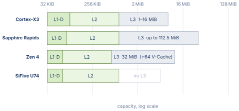
Figure 1 draws the four hierarchies to scale.
L1 caches
The U74 has a 32 KiB L1 instruction cache (two-way set-associative) and a 32 KiB L1 data cache (four-way set-associative). Line size is 64 bytes on both. Replacement on the L1 instruction cache is pseudo-random, a choice the U74 manual notes performs within a couple of percent of LRU for typical instruction streams, whose largely sequential fetch pattern leaves a recency-based policy little to exploit. The L1 data cache is true LRU, which stays affordable at four ways because the ordering fits in a handful of bits per set.
L2 cache (per-cluster, configurable)
The U74 L2 is shared across the cluster (up to four U74 cores) and is configurable in size from 128 KiB up to 8 MiB depending on the integrator’s choice. The L2 is eight-way set-associative. The L2 is inclusive of the L1s. Replacement is pseudo-random.
The U74 manual lists a load-to-use latency of around 30 cycles on an L2 hit. There is no shared L3 stage. The L2 is the last-level cache, after which requests go directly to the external memory controller. The choice to omit L3 is consistent with the U74’s deployment in cost-sensitive embedded Linux platforms where the area budget for SRAM is tight.
Implications of the missing L3
Workloads that exceed the L2 footprint pay a direct DRAM latency penalty without the benefit of an intermediate stage. For typical embedded workloads, the working set fits in L2 and the missing L3 is invisible. For workloads with larger footprints (large compile jobs, in-memory databases), the U74 is the wrong part. The deployment target makes the choice correct for the market it serves.
06.Side-by-Side Comparison
Reading the four parts in sequence shows where the textbook abstractions converge and where they diverge. The comparison table below collects the headline parameters into one view. All numbers come from the public sources cited in the per-part sections. Numbers vary by SKU. The table records the default documented configuration on the flagship part of each family.
Table 1. Cache hierarchies in four representative parts.
| Cortex-X3 | Sapphire Rapids | Zen 4 | SiFive U74 | |
|---|---|---|---|---|
| L1-I size | 64 KiB | 48 KiB | 32 KiB | 32 KiB |
| L1-I assoc | 4-way | 8-way | 8-way | 2-way |
| L1-I latency | 1 cycle | 5 cycles | 4 cycles | 1 cycle |
| L1-D size | 64 KiB | 48 KiB | 32 KiB | 32 KiB |
| L1-D assoc | 4-way | 12-way | 8-way | 4-way |
| L1-D latency | 4 cycles | 5 cycles | 4 cycles | 3 cycles |
| L2 size | 1–2 MiB | 2 MiB | 1 MiB | 128 KiB–8 MiB |
| L2 assoc | 8-way | 16-way | 8-way | 8-way |
| L2 latency | 14 cycles | 15 cycles | 14 cycles | 30 cycles |
| L2 inclusion | non-incl | non-incl | inclusive | inclusive |
| L3 size | 1–16 MiB | up to 112.5 MiB | 32 MiB (+64 V-Cache) | none |
| L3 assoc | 16-way | 16-way | 16-way | — |
| L3 latency | 30–40 cycles | 30–60 cycles | 50 cycles | — |
| L3 inclusion | NINE | non-incl | non-incl | — |
| L4 / HBM | none | 64 GiB HBM (Max SKUs) | none | none |
| LLC replacement | RRIP-family | QLRU-like | QLRU | pseudo-random |
| Sharing scope | cluster (DSU) | socket (mesh) | per-CCD | cluster |
Several patterns emerge. The L1 sizes have converged on the 32–64 KiB range with associativity between two and twelve. The private L2 sits at 1–2 MiB on the three high-performance parts, while the U74’s cluster-shared L2 is configurable across a far wider 128 KiB to 8 MiB range because it doubles as the last-level cache. The L3 has fanned out the most. The smartphone part stops at 16 MiB. The server part scales to over 100 MiB. The desktop X3D part stacks a die to reach 96 MiB per CCD. The embedded RISC-V part skips L3 entirely.
Inclusion policy has converged on non-inclusive (or NINE) at the LLC across the three commercial parts that have an L3, despite the LLC differing in how it is sliced and shared. Inclusive L2 behavior survives at AMD (where the L2 doubles as the snoop filter book) and at the bottom end (U74, where the L2 is the last cache and inclusion costs nothing). Non-inclusive L2 is the choice at ARM and Intel, where the L2 is private and the L3 holds the shared coherence state.
Replacement has moved away from true LRU at the L2 and L3 stages in every commercial part. The reasons are well-studied. True LRU is robust on workloads with strong temporal locality. It performs poorly on streaming and on scan-heavy workloads, where the working set never repeats. RRIP and QLRU and their relatives are better on average across a mix of workloads, at a slightly higher implementation cost. The textbook treatment in Chapter 38 laid out the analytic justification.
Prefetching has grown in importance generation over generation. Every high-performance part runs multiple hardware prefetchers (six on Sapphire Rapids, comparable counts on Zen 4 and Cortex-X3), with each engine specialized for a different access pattern. The U74 has a simpler stream prefetcher only. The differential reflects the workload mix the parts target: server and flagship phone workloads have richer memory-access patterns that justify a wider prefetcher portfolio.
The HBM-as-L4 mode on Sapphire Rapids is unique in the case study set. It extends the cache hierarchy beyond the SRAM boundary into stacked DRAM, anticipating a future where the next level beyond LLC is not external DDR but on-package high-bandwidth memory configured as cache.
07.Public-Source Discipline
This chapter relied exclusively on public sources. The ARM Technical Reference Manuals for Cortex-X3 and Cortex-X4 are downloadable from the ARM developer website. The Intel SDM and the companion Optimization Reference Manual are downloadable from Intel’s developer pages and are reissued every microarchitecture generation. The AMD Software Optimization Guide for Zen 4 is downloadable from AMD’s developer pages, again reissued per architecture. The SiFive U74 Core Complex Manual is downloadable from SiFive’s product pages. HotChips presentations and the IEEE proceedings of the conference are archived publicly.
The case for using public-only sources is not just an ethical one. It is also methodological. A reader who wants to verify any claim in this chapter can download the same documents the chapter relied on and reach the same conclusions. A reader who wants to extend the analysis (adding a fifth part, drilling deeper into one structure, computing AMAT for a specific workload) can do so from the same starting material. Public sources are reproducible. Proprietary sources are not.
The chapter also avoided several categories of claim that would require non-public data. It does not give exact RTL-level implementation details (those are confidential to each vendor). It does not benchmark against competitive parts on benchmark suites where the cited score depends on undisclosed compiler settings (a common pitfall in vendor marketing). It avoids any claim about future products. The reader gets a defensible, reproducible picture of the four parts as they ship today.
08.Worked Examples
09.Exercises
References
- [1](2022). “Arm.”
- [2](2023). “Arm.”
- [3](2024). “Intel.”
- [4](2023). “Software Optimization Guide for the AMD.”