DRAM and Memory Controllers
September 8, 202625 min readadvanced
This delicate physics has costs. A DRAM access takes tens of nanoseconds, two orders of magnitude longer than an L1 cache hit. The DRAM array consumes power merely to refresh, milliwatts per DIMM even when no…
The DRAM that backs main memory in every modern computer stores each bit as charge on a capacitor measured in femtofarads. A standard 6F DRAM cell is roughly nanometers in a 1z-node process and holds about 20 femtocoulombs of charge in the logic-1 state. Reading the bit drains the capacitor, so the read circuit must rewrite the value to restore the charge. Capacitors leak, so every row must be re-read and rewritten periodically before it forgets. The whole technology is held together by analog engineering at the femtoamp scale while presenting a clean digital interface to the memory controller.
This delicate physics has costs. A DRAM access takes tens of nanoseconds, two orders of magnitude longer than an L1 cache hit. The DRAM array consumes power merely to refresh, milliwatts per DIMM even when no program is touching memory, and the throughput is bounded by the analog timing of the sense amplifier circuit. Yet DRAM remains the densest, cheapest, fastest form of random-access storage in commercial volume. Replacing it has been the holy grail of memory research for forty years, with no replacement yet shipped at scale.
This chapter develops DRAM from first principles. It starts with the 1T1C cell, walks through the analog row activation sequence, covers the multi-level organization (cell, row, bank, rank, channel), develops the DDR and HBM timing protocols, and closes with the controller scheduling algorithms that decide which DRAM operation to issue next. Understanding why DRAM latency dominates cache miss penalty (covered abstractly in Chapter 36) requires looking at the analog physics of the row activation cost.
01.The 1T1C Cell
A single DRAM cell stores one bit as charge on a small capacitor. A pass transistor controls whether the capacitor connects to the bit line, the long metal wire that carries data into and out of the array. The gate of the pass transistor is driven by the word line, which is asserted when the row is activated.
A concrete numerical example clarifies the picture. The storage capacitor in a modern 1y-node DRAM holds about 25 femtofarads. Stored at 1.0 volts, this is femtocoulombs of charge. The bit line that the cell shares with the rest of the column has roughly 50 femtofarads of parasitic capacitance (about twice the cell capacitance, by design). When the word line opens, the cell capacitor shares its charge with the bit line. If the bit line was precharged to volts before the access, the resulting voltage on the combined capacitance is
For our numbers, V. The bit line moves from 0.5 V toward 0.667 V, a swing of just 167 millivolts. If the cell held a 0 (stored at 0 V), the corresponding shared voltage is V, a swing of mV from the precharge.
The sense amplifier attached to the bit line detects this small differential, amplifies it to the full rail voltage ( for a 1, 0 V for a 0), and drives the amplified value back onto the bit line. This restores the capacitor’s charge. Without the rewrite, the cell would emerge from the access at 0.667 V instead of 1.0 V, and the next read would yield an even smaller swing, eventually crossing into the 0 region. Every read is also a write because the read drains the cell.
The sense amplifier is not just a comparator. It is a back-to-back inverter pair (a positive-feedback amplifier) connected to two bit lines: the active bit line carrying the cell signal, and a complementary bit line carrying the precharge reference. When the amplifier is enabled, the small differential triggers regenerative positive feedback that pulls one bit line to and the other to ground. This is fast, but it is also why DRAM cannot be made arbitrarily small: shrinking the cell capacitor below about 20 fF makes the differential too small to reliably trigger the amplifier above the noise floor.
02.Row Activation and the Open Row
A DRAM access is not random. The unit of access at the array is the row, a wide horizontal slice of the array. A typical DRAM row holds 8192 bits in a single x8 chip (equivalent to 1024 bytes per chip, 8 KiB per 64-bit DIMM). Activating a row asserts the word line, opens the pass transistors for all cells in the row simultaneously, and dumps the charge from 8192 cells onto 8192 bit lines in parallel. The sense amplifiers amplify all 8192 differentials at once, then hold the amplified data in a row buffer.
Once a row is open, the controller can issue column commands to read or write specific bytes from the row buffer at much lower latency than the row activation itself. A typical sequence is
-
Precharge the bit lines to (this is the default state when no row is active). Time: , typically 13 ns.
-
Activate the row (assert word line, share charge, sense and amplify). Time: from activation to column ready, typically 13 ns.
-
Issue a column read. The selected bytes are driven from the row buffer through the bit-line sense amps to the chip output. Time: , typically 13 ns.
-
Optionally, issue more column reads while the row remains open. Each subsequent column hits in only , typically 4 ns.
-
When the controller decides to close the row, precharge again.
A row that is currently sensed and held by the sense amplifiers is called an open row. Accessing data in an open row costs only (around 13 ns for a column read). Accessing data in a different row requires precharging the open row (), activating the new row (), and then reading (). This three-step sequence is called a row miss and costs ns. An access that hits the currently-open row is a row hit and costs only ns.
The row hit advantage is a factor of three for typical DDR5 timings. A workload that streams sequentially through memory has near-perfect row hits because consecutive accesses lie in the same row. A workload with random pointer-chasing has near-zero row hits and pays the full row-miss latency on almost every access. The controller’s job is to maximize the row hit rate by reordering requests, covered later in this chapter.
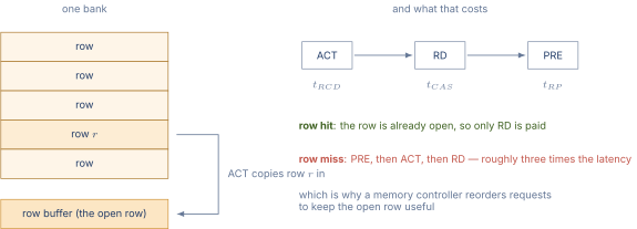
Figure 1 shows where the time goes.
03.Banks, Ranks, Channels
A single DRAM array organized as one large row of bit lines would be slow. Activating an 8 KiB row dumps charge from 64,000 cells simultaneously, draining significant supply current and producing significant noise. Real DRAM organizes the storage hierarchically.
The unit of independent operation within a DRAM chip is the bank. A modern DDR5 chip has 32 banks organized as 8 bank groups of 4 banks each. Each bank can have its own open row, and the controller can overlap operations across banks: activate row R0 of bank 0, then read column 3 of bank 0 while issuing activate for row R0 of bank 1, and so on. This bank-level parallelism is the primary source of DRAM throughput.
A rank is a group of DRAM chips on a DIMM that share the data bus. A 64-bit DIMM typically has 8 chips, each contributing 8 bits to a 64-bit-wide word (this is the x8 configuration, while x4 chips give a 16-chip rank and x16 chips give a 4-chip rank). All chips in a rank are accessed in parallel: an activate command goes to the same row in every chip, and a column read returns 8 bits from each chip simultaneously, assembling the 64-bit word.
A channel is a complete memory bus with its own command, address, and data signals. A modern server CPU has 8 or 12 channels. Each channel can hold one or two DIMMs (one or two ranks per DIMM). Channels operate fully in parallel, so a 12-channel system has 12 independent memory operations in flight at once at the channel level, with bank-level parallelism stacking on top of that.
The full hierarchy on a DDR5 system with 12 channels, 2 ranks per channel, 32 banks per chip, and 8 chips per rank yields independent banks total. Achieving high parallel utilization across all of them is the central job of the memory controller.
Table 1. Bank and channel counts in five representative memory configurations. Each row assumes one rank per channel, so the total-banks column is channels times banks per chip. Data drawn from the JEDEC DDR4/DDR5 standards and HBM3 product briefs.
| Configuration | Channels | Banks/chip | Width (bits) | Total banks |
|---|---|---|---|---|
| Consumer DDR4 (dual channel) | 2 | 16 | 64 | 32 |
| Server DDR5 (12 channel) | 12 | 32 | 64 | 384 |
| GDDR6X (RTX 4090) | 12 | 16 | 32 | 192 |
| HBM3 (1 stack) | 16 | 32 | 64 | 512 |
| HBM3 (6 stacks) | 96 | 32 | 64 | 3072 |
04.DDR Timing Parameters
The JEDEC standards for DDR4 and DDR5 specify dozens of timing parameters that the controller must respect. A few are central to performance.
(row-to-column delay). The time from issuing an activate to when the first column read can be issued. Typically 13 to 15 ns. Sets the floor on the row-miss latency.
(column latency, CAS latency). The time from issuing a column read to when the data appears on the bus. Typically 13 to 15 ns for DDR5, 15 to 19 ns for DDR4. Set on the DIMM SPD chip and selected by the controller during training.
(row precharge). The time from issuing a precharge to when the array can be activated again. Typically 13 to 15 ns.
(row active time). The minimum time a row must remain open after activation, set by the analog refresh operation that the sense amplifier performs. Typically 32 ns.
(row cycle time). The minimum time between two activations of the same bank. Equals , typically 45 to 50 ns. Bounds the activate rate per bank.
(refresh interval). The average interval between refresh commands. Typically 7.8 us at room temperature, 3.9 us at extended temperature. Each row must be refreshed every 64 ms (32 ms at extended temperature).
(four-activate window). The minimum time during which only four activates can be issued across all banks. Limits the peak power dissipated during bursts of activates. Typically 15 to 25 ns.
These timings are inelastic. The controller can issue commands back-to-back only if it has tracked the elapsed time since the previous command to each bank and verified that all relevant timings have been satisfied. This is why memory controllers maintain per-bank state machines and command queues rather than issuing commands directly from the cache.
DDR5 improves on DDR4 by running the bus at twice the frequency, doubling the bank count, and splitting the 64-bit channel into two independent 32-bit sub-channels. The narrower sub-channel doubles the burst length to 16 transfers per 64-byte cache line, against DDR4’s 8 transfers over a full 64-bit channel, because each sub-channel has to move the whole line on its own. The peak bandwidth doubles at the same DIMM count. The latency improves modestly because the analog timings of the DRAM array do not shrink as fast as the bus speed grows. This is the classic DRAM story: bandwidth scales, latency does not.
05.LPDDR and HBM
Two variants of the DDR family are worth covering in detail because they appear in mobile devices (LPDDR) and high-bandwidth applications (HBM).
LPDDR5 and LPDDR5X. Low-power DDR5 is the DRAM standard for smartphones, tablets, and increasingly laptops (Apple Silicon, Qualcomm Snapdragon X, Intel Lunar Lake). Key differences from standard DDR5: a narrower 16-bit channel (vs 64-bit), more channels (up to 16 per package in Apple silicon), much tighter clock gating, and deeper power-down states. The on-die ECC array that corrects single-bit errors without exposing the cost to the memory controller is not one of the differences, because JEDEC makes on-die ECC mandatory for standard DDR5 as well. LPDDR5X pushes data rates to 8533 MT/s. The smaller channel width reduces the energy per bit moved because fewer drivers switch on each access.
HBM3 and HBM3E. High Bandwidth Memory is a vertically stacked DRAM technology with up to 16 channels per stack and short, fast TSV (through-silicon via) interconnects to the host die. A single HBM3 stack delivers up to 819 GB/s. GPU accelerators typically integrate 4 to 8 stacks for aggregate bandwidth in the multi-TB/s range (NVIDIA H100 has 5 stacks for 3.35 TB/s, NVIDIA B100 has 8 stacks for 8 TB/s). HBM’s combination of width (16 channels per stack) and short interconnect length (millimeters rather than centimeters) enables both higher bandwidth and lower energy per bit than DDR or LPDDR. The cost is high: HBM stacks require advanced packaging (silicon interposers or fan-out wafer-level packaging) that adds significantly to the cost per GB.
Table 2. Bandwidth and latency comparison across DRAM technologies. Latency figures are for unloaded row-miss access, and bandwidth is per package or stack. Sourced from JEDEC standards and product briefs.
| Technology | Bandwidth | Latency (ns) | Use case |
|---|---|---|---|
| DDR4-3200 | 25.6 GB/s | 50 to 70 | Desktop, server (legacy) |
| DDR5-6400 | 51.2 GB/s | 40 to 60 | Desktop, server (current) |
| LPDDR5X-8533 | 17.1 GB/s (16-bit) | 50 to 80 | Mobile, laptop |
| GDDR6X-21000 | 84 GB/s (32-bit) | 70 to 100 | Discrete GPU |
| HBM3-6400 | 819 GB/s (per stack) | 100 to 150 | Datacenter GPU |
06.Refresh
Capacitors leak. A DRAM cell holds its stored charge for tens of milliseconds at room temperature before the leakage drops the voltage below the sense margin. The JEDEC standard mandates that every row be refreshed at least every 64 ms (32 ms at extended temperatures above 85 C). A standard DDR5 chip has 65,536 rows per bank, which means the controller must refresh rows at an average rate of rows/ms, or one row per bank roughly every 1 us.
The controller issues a REF command that the DRAM chip uses to refresh several rows from each bank in parallel. A DDR5 REF command covers 8 rows in every bank, 256 rows in total across the 32 banks, so 8192 REF commands walk all 65,536 rows of a bank once. Spreading those 8192 commands across the 64 ms window puts one REF every us, the standard value for DDR5 at room temperature.
A REF command stalls all banks for (refresh cycle time), typically 350 ns to 500 ns. During those 500 ns, no other DRAM access can proceed. At us, the controller spends about percent of its bus time on refresh. At extended temperatures with us, refresh consumes nearly 13 percent of bus time.
Postponed refresh. Real controllers can defer refresh slightly so that high-priority accesses can issue first. The DDR5 standard allows refresh deferrals of up to 8 commands, which lets the controller absorb bursts of latency-sensitive traffic and batch refreshes during quieter periods.
Fine-grain refresh. DDR4 added 2x and 4x fine-grain refresh modes that issue more REF commands with shorter each. The overhead is similar but the worst-case latency per refresh is smaller, which helps real-time workloads. DDR5 made fine-grain refresh the default.
Per-bank refresh. HBM3 supports per-bank refresh that stalls only the bank being refreshed, leaving the other 31 banks free. This is feasible because HBM’s wider channel and lower per-bank load make the analog timing of a single-bank refresh more self-contained. DDR5 currently does not offer per-bank refresh, though it is on the JEDEC roadmap.
07.Memory Controllers and Scheduling
The memory controller sits between the cache hierarchy and the DRAM, accepting requests from the cache and issuing the appropriate sequence of DRAM commands to satisfy them. Its responsibilities are several.
Address mapping. The controller maps the cache line address (typically a 64-byte address) to a tuple of (channel, rank, bank group, bank, row, column). The mapping is configurable and is chosen to maximize parallelism for typical workloads. A common mapping puts low-order address bits into the column to keep consecutive cache lines in the same row (favoring streaming accesses), the next bits into bank and bank group to spread parallel accesses across banks (favoring scatter accesses), and the high bits into the row. This is summarized in the table below.
Request scheduling. The controller has a queue of pending requests and a state machine tracking the timing constraints of each bank. It picks the next command to issue from among the ready requests. The canonical policy is FR-FCFS, first-ready first-come-first-served. A request is ready if all its DRAM timing constraints are satisfied (the bank is not refreshing, has elapsed since the last activate to the same bank, etc.). Among ready requests, FR-FCFS prefers those that hit the currently open row. Among row-hit requests, FR-FCFS prefers the oldest. This balances throughput (row hits are cheaper) against fairness (the oldest request eventually issues).
Row policy. After a column read, the controller can either leave the row open (an open-page policy) or precharge immediately (a close-page policy). Open-page wins when consecutive accesses to the same bank are likely to hit the same row (streaming workloads). Close-page wins when consecutive accesses to the same bank are likely to hit different rows (scattered workloads). Real controllers use an adaptive page policy that switches based on recent hit rates.
Table 3. Typical DDR5 address mapping for a 12-channel system with 32 banks per chip. Low-order bits change first, so consecutive cache lines tend to fall in the same row but different columns.
| Address bits | Field | Function |
|---|---|---|
| 0:5 | Byte in cache line | Selects byte within 64 B line |
| 6:9 | Column low | Selects 64 B chunk within row |
| 10:13 | Channel | Spreads across 12 channels |
| 14:18 | Bank & bank group | Spreads across 32 banks |
| 19:21 | Column high | Remaining columns in row |
| 22:37 | Row | Selects DRAM row |
| 38+ | Rank, chip | Selects rank in higher-order config |
Read-write reordering. Switching from reads to writes incurs a delay (, read-to-write), and switching from writes to reads incurs another (, write-to-read). Controllers batch reads and writes to amortize the switch. A typical scheduling policy processes a batch of reads until the queue empties or a deadline is reached, then processes a batch of writes until the write queue is empty or a fairness threshold is reached.
Refresh integration. The refresh schedule is woven into the command stream. REF commands have priority on average but can be deferred up to 8 commands behind reads, so the controller has some flexibility to batch refreshes during quiet periods.
Idealized FR-FCFS scheduler in pseudocode.
typedef struct { addr_t addr; int age; bool read; } req_t;

req_t schedule(req_t *queue, int n, state_t *banks) {
    req_t *best = NULL;

    /* Pass 1: prefer ready, row-hit requests */
    for (int i = 0; i < n; i++) {
        if (!ready(queue[i], banks))           continue;
        if (!hits_open_row(queue[i], banks))   continue;
        if (best == NULL || queue[i].age > best->age)
            best = &queue[i];
    }
    if (best != NULL) return *best;

    /* Pass 2: any ready request, oldest first */
    for (int i = 0; i < n; i++) {
        if (!ready(queue[i], banks)) continue;
        if (best == NULL || queue[i].age > best->age)
            best = &queue[i];
    }
    if (best != NULL) return *best;

    /* Pass 3: issue a precharge or activate to make progress */
    return choose_speculative(queue, n, banks);
}08.Why DRAM Latency Dominates Miss Penalty
The miss penalty referenced repeatedly in Chapter 38 is fundamentally the DRAM access time. A typical loaded DRAM access (queued behind other requests, missing the row buffer, paying the activate + read sequence) is 60 to 100 ns end to end. At a 3 GHz CPU clock, this is 180 to 300 cycles. Even a row-hit access at ns plus a few nanoseconds of traversal on the DRAM bus itself is 50 to 60 cycles measured at the device, before the interconnect and return-path costs itemized below are added on top.
The components of the latency break down roughly as
-
L3 miss to memory-controller request: 10 to 20 ns (mostly bus arbitration and the on-die mesh that connects cores to memory controllers on modern chips).
-
Memory controller queue and scheduling: 5 to 30 ns (depends on load).
-
DRAM access (row miss, no contention): ns.
-
Return path from DRAM through controller to L3 to L2 to L1: 10 to 20 ns.
Total: 64 to 109 ns for a row miss without queueing, which is consistent with the 80 to 120 ns figure that modern benchmarks measure. Under load, the queueing delay can dominate: a memory-bound workload may see 200 ns or more on average.
The implication is stark. A core that misses to DRAM stalls for roughly 300 cycles. An out-of-order machine can paper over part of this by finding 300 cycles of independent work in the instruction stream, but only if such work exists (a register-limited code with a small reorder buffer cannot hide the miss). This is why memory prefetching (Chapter 40), cache hierarchies designed to maximize hit rate (Chapter 39), and software techniques like loop tiling and prefetch hints exist.