The Memory Wall
September 13, 202627 min readadvanced
The pipelined and superscalar processors of Part III run at frequencies above 3 GHz on modern silicon, completing one instruction every 333 picoseconds in steady state. A single load instruction that misses…
The pipelined and superscalar processors of Part III run at frequencies above 3 GHz on modern silicon, completing one instruction every 333 picoseconds in steady state. A single load instruction that misses every level of on-chip cache and reaches main memory takes roughly 70 nanoseconds round trip. In the time that one DRAM access completes, an idle processor could have retired two hundred instructions. The arithmetic of that gap is the entire premise of Part IV. No amount of pipelining, branch prediction, or out-of-order execution rescues a processor that has to wait for DRAM on every memory access. The architectural response is the memory hierarchy, which uses small fast storage close to the processor to filter the traffic that actually reaches the slow large storage farther away.
This chapter establishes the quantitative basis for the rest of the part. It introduces the locality property that makes hierarchical storage work, walks the levels of the modern pyramid with concrete latency and capacity numbers, and develops the central observation that DRAM latency has barely shrunk over four decades while processor frequencies have grown several thousandfold. The mismatch is the memory wall, and it is the binding constraint that shapes every higher-performance architecture from Chapter 37 onward.
01.A Numerical Walk Through One Access
Before introducing any abstractions, consider one concrete memory access on a modern desktop processor. A program executes the load instruction lw t0, 0(a1), asking for the 32-bit word whose address is held in register a1. Suppose a1 contains the address 0x4000_1080. The processor must deliver the contents of that address to register t0 before any instruction that depends on t0 can proceed.
If the data sits in the L1 data cache, the cache lookup takes about 4 processor cycles. At 3 GHz that is 1.3 nanoseconds. The dependent instruction stalls for four cycles, the load completes, and the pipeline keeps moving.
If the data is not in L1 but sits in the L2 cache, the lookup takes about 12 cycles, or 4 nanoseconds. The dependent instruction stalls for twelve cycles.
If the data is not in L2 but sits in the shared L3 cache, the lookup takes about 40 cycles, or 13 nanoseconds. The dependent instruction stalls for forty cycles.
If the data is not in any on-chip cache and must come from main memory, the access takes between 200 and 300 cycles. At 3 GHz that is 70 to 100 nanoseconds, and that figure already covers the memory controller and the on-chip interconnect as well as the DRAM access itself.
If the data is not in main memory and must come from a NVMe solid- state drive (a page fault), the access takes between 10 and 100 microseconds, which at 3 GHz is between 30,000 and 300,000 cycles.
If the data sits on a spinning magnetic disk, the access takes between 5 and 15 milliseconds. At 3 GHz this is between 15 million and 45 million cycles of stall.
The five ratios from L1 to disk span more than seven orders of magnitude. A processor that paid the full disk-access cost on every load would deliver effective throughput a hundred-millionth of its nominal IPS. The reason real programs do not see this catastrophe is that the cost distribution is highly skewed. Most loads hit in L1, very few reach DRAM, and almost none touch disk during steady- state execution. The skew is not accidental. It is engineered by the locality property of programs, which the rest of this chapter makes precise.
02.Locality: Why the Hierarchy Works
The memory hierarchy is engineering, not magic. Its premise is an empirical regularity in real programs that computer architects have relied on since the 1960s. That regularity has two facets.
Temporal Locality
A program exhibits temporal locality when an address that was accessed once is likely to be accessed again soon. The simplest example is a loop induction variable. Consider the following loop:
Sum of array elements
| int sum = 0; | |
| for (int i = 0; i < N; i++) { | |
| sum += a[i]; | |
| } |
The variables sum and i are read and written on every iteration. If the loop body executes one million times, each of those two locations is touched two million times. Without any caching, every one of those accesses would pay full DRAM latency. With even the smallest cache, the second iteration finds both variables already loaded and pays only L1 latency. The compiler typically keeps both variables in registers, which is the extreme case of temporal locality exploitation, but the principle is the same. A handful of locations carry most of the access traffic.
Spatial Locality
A program exhibits spatial locality when an access to address is followed soon by accesses to addresses near . The array sum loop above accesses a[0], a[1], a[2], ... in sequence. If a is a contiguous array of 4-byte integers, those accesses are 4 bytes apart. The DRAM that holds a can deliver a 64-byte cache line in a single burst, paying the access latency once and then streaming sixteen consecutive integers at full memory-channel bandwidth. Without spatial locality this batching would have no payoff, because each integer would require its own DRAM access. With spatial locality the first miss in the cache line pays the full DRAM latency and the next fifteen accesses are free.
Both Together
Real programs exhibit both forms of locality at once. An array sum has temporal locality on the accumulator and the loop counter, and spatial locality on the array. A binary tree traversal has temporal locality on the root of the tree (touched on every traversal) and weaker spatial locality on the deeper nodes (which may be scattered in memory). A linked list has weak spatial locality (because the next-pointer can point anywhere) but may have temporal locality if the same list is traversed repeatedly.
The strength of locality varies by workload. SPEC integer benchmarks hit in L1 with rates between 95 and 99 percent. Graph traversal codes can hit L1 with rates as low as 60 percent. The architectural response is the same in both cases. Put a small fast cache near the processor to capture the temporal and spatial hot spots. Let the hot spots that miss reach a larger slower cache. Send only the genuinely cold misses out to DRAM.
03.The Memory Pyramid
The classical depiction of the memory hierarchy is a pyramid, with fast small expensive storage at the top and slow large cheap storage at the bottom. Figure 1 shows the modern shape. The numbers come from publicly available vendor data sheets and from the SPEC CPU2017 results database.
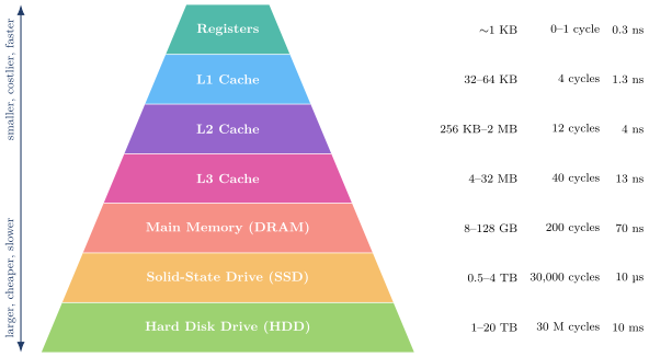
The seven levels span more than seven orders of magnitude in latency, ten orders of magnitude in capacity, and nearly five orders of magnitude in cost per byte. The geometric pattern is no accident. Each level exists because the level above it is too small to hold the working set of typical programs, and the level below it is too slow to serve the residual access traffic at full processor speed.
Registers
The register file is the topmost level. A typical RV64I implementation exposes 32 integer registers, each 8 bytes, for 256 bytes of architecturally visible state. With a separate floating-point file and the program counter, the total is closer to 600 bytes. Register reads complete in the same cycle as the instruction that needs them (through register-file read ports), giving an effective latency of zero cycles. The cost is paid in chip area and in the encoding budget of the ISA, since each register name consumes 5 bits in the instruction word.
L1 Caches
The level-1 cache sits one stage below the register file. Modern designs split L1 into separate instruction and data caches (the Harvard split), each typically 32 or 64 KB. Access takes 4 cycles in pipelined designs, set by the time to read a SRAM array, decode the address, compare tags, and forward the result to the execution unit. At 3 GHz this is 1.3 nanoseconds.
The L1 is private per core. On an eight-core processor there are sixteen L1 caches (eight instruction, eight data), each independently serving its own core. Per-core privacy avoids contention on the hottest access path, at the cost of needing a coherence protocol to keep duplicate copies of shared data consistent across cores. Chapter 39 previews the coherence problem, and a full treatment of the protocol lies beyond this book.
L2 Cache
The level-2 cache sits below L1. Typical sizes are between 256 KB and 2 MB per core. Access takes between 10 and 14 cycles. Most modern designs make L2 private per core (one L2 instance per L1 pair), though some older designs and some little-core designs share L2 across two or four cores.
The L2 is the first level designed to catch misses that L1 cannot absorb. A program with a working set of 800 KB does not fit in a 64 KB L1, so most accesses miss L1. If the program fits in a 1 MB L2, those misses cost about 12 cycles each, not the 200 cycles a DRAM access would impose. The cost difference matters. A 12-cycle miss is annoying. A 200-cycle miss is catastrophic.
L3 Cache
The level-3 cache (sometimes called the last-level cache, or LLC) is shared across all cores on the same die. Sizes range from 4 MB on low-end designs to over 100 MB on server processors. Access takes between 30 and 60 cycles.
The L3 plays two roles. First, it absorbs working sets that exceed the L2 size of any single core. Second, it serves as the coherence choke point through which all inter-core memory traffic flows. A core that wants to read a cache line currently held by another core issues a coherence request to the L3, which forwards the request to the holder. The L3’s role in coherence is one of the reasons it is shared rather than private.
Main Memory (DRAM)
Main memory is built from DRAM chips connected to the processor through a memory controller. Capacities range from 8 GB on consumer laptops to 6 TB on flagship servers. Access latency is between 50 and 100 nanoseconds, which at 3 GHz works out to 150 to 300 processor cycles.
A 64 GB DDR5-6400 channel offers about 51.2 GB/s of peak bandwidth. Modern processors typically have two to twelve channels, for an aggregate of 100 GB/s to 600 GB/s of memory bandwidth. The cost per gigabyte is roughly 3 USD in mid-2024, roughly thirty times cheaper than the SRAM that makes up the L3.
Solid-State Drive
The SSD layer holds files that do not fit in DRAM. Modern NVMe SSDs offer between 0.5 and 4 TB of capacity and access latencies of 10 to 100 microseconds. The bandwidth of a PCIe Gen5 NVMe drive can reach 12 GB/s, which is comparable to a single DRAM channel but spread over an access that costs tens to hundreds of thousands of cycles. The SSD is the working tier for virtual memory and for file system data that the program references through demand paging.
Hard Disk Drive
The bottom of the pyramid holds archival storage. A spinning magnetic disk has a head that must physically move across the platter to reach the requested data. Mechanical seek and rotational delay sum to between 5 and 15 milliseconds. At 3 GHz this is 15 to 45 million processor cycles. HDDs survive in the storage hierarchy because their cost per gigabyte (about 0.02 USD in 2024) is about five times cheaper than SSDs. They are inappropriate as a paging tier for an interactive workload but excellent for infrequently accessed archives.
04.The Memory Wall
The pyramid in the previous section is the static picture of the modern memory system. To see why this picture exists at all, the historical record matters. Figure 2 plots processor clock frequency and DRAM access latency from 1980 through 2024.
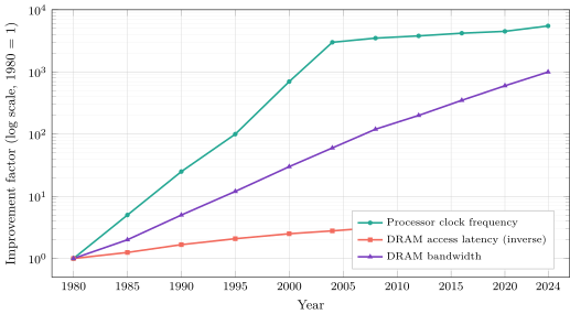
Three curves tell the story. Processor clock frequency grew by roughly 5500x between 1980 and 2024, with most of that growth concentrated between 1985 and 2005. DRAM bandwidth grew by roughly 1000x, driven by wider buses and higher-speed signaling. DRAM latency improved by only about 3.6x, from roughly 250 ns to roughly 70 ns, and most of that improvement happened before 2000. The bandwidth and frequency curves track each other within an order of magnitude. The latency curve is not merely behind them, it is on a different scale entirely, and that separation is the memory wall.
The comparison is only fair if latency is measured end to end. A DDR5 device quotes a column-access time of roughly 12 ns, and citing that number instead would suggest a 21x improvement. But the 250 ns figure for 1980 is a full random access, so the honest comparison uses full random access at both ends. Column access is one component of the path, not the path.
Why DRAM Latency Has Not Shrunk
DRAM latency is set by the physics of the storage cell. A DRAM bit is a single capacitor connected through an access transistor to a sense line. Reading the bit requires precharging the sense line, activating the access transistor, allowing the capacitor’s charge to redistribute onto the sense line, and amplifying the resulting small voltage difference to a clean digital level. The capacitor itself is a few femtofarads. The sense line carries thousands of other bits and has hundreds of picofarads of parasitic capacitance. The charge redistribution and amplification steps cannot be made much faster without changing the cell structure. Decades of process shrinks have made the cell smaller, increased density, and reduced energy per access, but the time to sense a row has stayed in the 30-to-60 nanosecond range since the early 1990s.
Bandwidth, by contrast, can be improved by parallelism. Adding channels, widening buses, increasing signaling frequency, and prefetching adjacent rows all multiply the byte rate. A modern DDR5-6400 module delivers 51.2 GB/s on a 64-bit bus running at 6400 MT/s, even though the latency to fetch a single random word is still around 70 nanoseconds. Latency is set by the slow first access. Bandwidth is set by how many accesses overlap.
Why Processor Frequency Stalled
The second half of the gap is the processor side. Clock frequency grew rapidly from 1980 through about 2004, reaching 3.8 GHz on the Intel Pentium 4 Prescott. After 2005, frequency stayed roughly flat. The reason is power, not the inability to clock faster. The Pentium 4 Prescott dissipated 115 W at 3.8 GHz on the 90 nm process. Pushing the same architecture to 5 GHz would have required higher voltage and would have driven power past the 200 W ceiling that desktop thermal solutions could handle. The industry pivoted to multi-core designs that traded frequency for parallelism.
The frequency stall did not close the gap. The single-thread performance of a modern core continues to grow through deeper pipelines, wider issue widths, smarter branch predictors, and larger out-of-order windows. Each of these improvements raises the demand for memory bandwidth and shortens the tolerable latency. The widening gap in Figure 2 reflects this demand-side growth as much as the supply-side stall.
05.Bandwidth Versus Latency
A common confusion among newcomers to memory-system design is the relationship between latency and bandwidth. The two are independent properties that often trade against each other. A subsystem can have low latency and low bandwidth (a tiny SRAM with one read port), high latency and high bandwidth (a wide DRAM channel), or any combination in between.
Consider a memory channel that delivers a 64-byte cache line in 70 nanoseconds. The latency for any single request is 70 ns. If the channel can serve only one request at a time, the bandwidth is . But real DRAM channels overlap many requests. A modern memory controller can have 30 or more requests in flight simultaneously. If the channel serves 30 requests in 70 ns total (because the requests overlap), the bandwidth is . The latency of any one request is unchanged. Only bandwidth improved.
The key relationship is Little’s law, which appears throughout queueing theory. If a system has average latency seconds per request and bandwidth of requests per second, the average number of requests in flight at steady state is
A DRAM channel at 25 GB/s with a 70 ns single-request latency must have an average of requests in flight to sustain that bandwidth. If the processor cannot generate 27 simultaneous outstanding memory requests, the channel goes underutilized and the effective bandwidth drops.
Why Bandwidth Has Improved Faster
The historical trend in Figure 2 reflects a fundamental asymmetry. Bandwidth scales with parallelism. Add more channels, widen each bus, run at higher signal rates, and the byte rate multiplies. Latency does not scale with parallelism in the same way. The single-cell sensing time is a fixed cost that no amount of parallelism reduces. The bandwidth curve has a slope close to Moore’s-law density scaling, while the latency curve flattens against the cell-physics ceiling.
The architectural consequence is that bandwidth-bound workloads have a clear path forward. Adding memory channels, using HBM stacks, and improving the interconnect all help. Latency-bound workloads do not have the same path. A pointer-chasing workload that touches a random new cache line on every dependent load is limited by single-request DRAM latency, and that latency has barely moved in twenty years.
06.Cost, Capacity, and Why the Hierarchy Stays Layered
The reason architectures use a layered hierarchy rather than one huge fast memory is economics combined with physics. A few representative numbers from mid-2024 make the case.
Table 1. Cost, capacity, and latency of storage levels in 2024. SRAM and DRAM cost figures are die-area-based estimates. SSD and HDD figures are end-user retail prices. Source: Hennessy and Patterson� , Table� 2.2, updated with public 2024 data.
| Technology | Capacity per chip | Latency | Cost (USD/GB) |
|---|---|---|---|
| SRAM (on-die L1) | 64 KB | 1.3 ns | 1000 |
| SRAM (on-die L3) | 32 MB | 13 ns | 100 |
| DRAM (DDR5) | 32 GB | 70 ns | 3 |
| NAND (NVMe SSD) | 4 TB | 30 μs | 0.10 |
| HDD (spinning disk) | 20 TB | 10 ms | 0.02 |
The cost-per-byte ratio between SRAM and DRAM is about 30 to 330 depending on the SRAM density used. The ratio between DRAM and SSD is about 30. The ratio between SSD and HDD is about 5. The hierarchy survives because no single technology delivers both the speed of SRAM and the capacity of an HDD at a tolerable cost. The architectural answer is to layer technologies so each level pays only for what the level below it cannot serve.
The hierarchy is also dictated by physics. An on-chip SRAM array shares the same die as the processor and can be read with a single clock-cycle’s worth of wire delay. Off-chip DRAM sits centimeters away through a printed circuit board trace, and the round-trip electrical signaling alone consumes tens of nanoseconds. The L3 cache exists in part because going off-chip is unavoidably slower than staying on-chip, regardless of the storage technology used.
When the Hierarchy Inverts
A workload that fits entirely in one level pays only that level’s latency. A 24 KB hash table fits in any L1 and accesses it at L1 speed. A 1 MB matrix fits in L2 and accesses it at L2 speed. The inversions come when the working set straddles a boundary. A 2 MB matrix on a processor with a 1.5 MB L2 sees nearly every access miss L2 and land in L3, paying 40 cycles per access instead of 12. The 33-percent capacity shortfall produces a 3x slowdown. Working- set sensitivity is one of the dominant performance concerns in high-end software, and Chapter 38 develops the quantitative tools for analyzing it.
07.The Architectural Response
The memory wall is not a problem any one technique solves. It is the constraint that shapes essentially every higher-performance architectural idea developed in the rest of this part and in Part V. This section previews the responses, each of which is the subject of a later chapter.
Caches (Chapter 37) are the foundational response. Place a small fast cache between the processor and the slow large memory. Exploit locality to keep the hottest data in the cache. Pay the slow latency only on the cold misses.
Cache performance analysis (Chapter 38) develops the quantitative tools. Average memory access time (AMAT) summarizes the cost of a memory access as a weighted sum of hit and miss times. Multi-level caches extend the analysis to two or three levels.
Advanced cache organizations (Chapter 39) cover the techniques that real designs use to push hit rates higher and to hide miss latency. Skewed associativity, way prediction, sectored caches, and dead-block prediction all attack different parts of the cost equation.
Prefetching (Chapter 40) attacks the latency directly. If the processor can predict an upcoming access and start the fetch early, the data arrives by the time the load instruction executes. A perfectly accurate and timely prefetcher converts every miss into a hit.
Out-of-order execution (Part V) attacks the gap from the demand side. While one load waits for memory, the processor keeps executing later independent instructions. The reorder buffer holds in-flight work and commits it in program order once the slow load completes.
Memory-level parallelism (Chapters 39 and 54) attacks bandwidth utilization. Issue many independent loads simultaneously so the memory controller can overlap them, sustaining bandwidth near the channel’s peak.
Each response is independent of the others, and modern designs deploy all of them simultaneously. The remainder of Part IV develops the cache and prefetching sides. Part V develops the out-of-order and memory-level-parallelism sides. The two parts are tightly coupled, and a graduate-level understanding of either requires familiarity with both.
08.Looking Ahead
The next chapter introduces caches from first principles. It covers direct-mapped, set-associative, and fully-associative organizations, the three Cs that classify all cache misses, and the write policies that govern how stores propagate through the hierarchy. The treatment is concrete throughout, with worked examples that compute the address breakdown and hit-or-miss outcome for specific load sequences.