I/O Architecture
September 8, 202623 min readadvanced
Computers are useful because they communicate with the outside world. Keyboards, mice, displays, network interfaces, storage devices, and specialized accelerators all need a path between their data and the…
Computers are useful because they communicate with the outside world. Keyboards, mice, displays, network interfaces, storage devices, and specialized accelerators all need a path between their data and the CPU’s address space. The mechanisms that connect peripherals to the CPU and memory form the I/O architecture of a system.
This chapter develops the I/O subsystem from first principles. It opens with the two ways CPUs talk to device registers (memory-mapped I/O and the older port I/O), develops the direct memory access mechanism that lets peripherals move bulk data without CPU intervention, introduces the IOMMU that translates device addresses and enforces isolation, walks through the PCIe interconnect that carries almost all modern peripheral traffic, introduces the Address Translation Services (ATS) and Page Request Interface (PRI) extensions that let PCIe devices participate in virtual memory the same way CPU cores do, and closes with Compute Express Link and the continuing integration of peripherals into the CPU’s memory and coherence model.
I/O architecture is where security, performance, and virtualization intersect. A poorly-designed DMA engine can read kernel memory. A poorly-isolated PCIe device can sniff traffic from a sibling device. A correctly-designed IOMMU enforces both. Modern systems take I/O isolation seriously because the consequences of getting it wrong are catastrophic.
01.Memory-Mapped I/O vs Port I/O
A CPU communicates with a device by reading and writing the device’s control registers. The device exposes registers for configuration, status, command, and data. A network card has registers for the MAC address, transmit queue head and tail, receive queue head and tail, interrupt mask, and so on. The CPU writes these registers to configure the device, reads them to check status, and triggers actions by writing command registers.
Two architectural conventions exist for how the CPU addresses these registers.
Port I/O. Intel x86 inherits from the original 8080 the idea of a separate I/O address space, widened on the 8086 to 65536 port addresses and accessed by the IN, INS, OUT, and OUTS instructions [1]. The address pins drive the same memory bus, but a separate signal (M/IO) distinguishes I/O from memory accesses. Each device is assigned a range of port numbers, and the CPU reads the device by issuing IN from a port number. This was the convention on the original PC architecture, with the legacy keyboard controller at ports 0x60 and 0x64, the legacy serial ports at 0x3F8 and 0x2F8, and so on.
Memory-mapped I/O (MMIO). Every other major architecture (RISC-V, ARM, MIPS, PowerPC, Alpha) uses memory-mapped I/O exclusively. Each device’s registers occupy a range of normal physical addresses, and the CPU accesses them through ordinary load and store instructions. The device decodes its assigned address range from the memory bus and responds to loads and stores as if it were memory, except that loads return device state and stores trigger device actions.
MMIO is the dominant convention in modern systems for several reasons. It removes a special instruction class from the architecture, simplifying the ISA. It works uniformly across 32-bit, 64-bit, and embedded systems. It allows devices to be mapped into virtual address spaces with the same protection mechanism that protects normal memory. It permits modern prefetching and out-of-order memory access optimizations to apply to device accesses (with care, since device registers have side effects on every read).
Even x86 has largely moved to MMIO for new devices. The legacy port-I/O space remains for backward compatibility with PC-era hardware, but PCIe devices, network controllers, GPUs, and storage controllers all use MMIO. The legacy I/O ports survive in firmware for early boot operations.
A concrete example clarifies MMIO usage. Suppose a serial UART has its control registers at physical address 0xFE00_2000. The transmit data register might be at offset 0, the status register at offset 4. Sending a byte involves the following sequence.
Idealized MMIO UART driver code.
#define UART_BASE     0xFE002000UL
#define UART_DATA     ((volatile uint32_t *)(UART_BASE + 0))
#define UART_STATUS   ((volatile uint32_t *)(UART_BASE + 4))
#define STATUS_TX_RDY (1u << 0)

void uart_putc(char c) {
    /* Wait for transmit register to be empty. */
    while ((*UART_STATUS & STATUS_TX_RDY) == 0)
        ;
    /* Write the byte to the data register, which clocks it out. */
    *UART_DATA = (uint32_t)c;
}
The volatile qualifier prevents the compiler from caching the load result in a register, since the value can change between reads. The address is mapped into the kernel virtual address space as uncached memory so that loads and stores bypass the data caches and reach the device on every access.
02.Direct Memory Access
MMIO is fine for small, infrequent device interactions. Transferring a megabyte from a network packet to a buffer in DRAM through a sequence of CPU loads from the device’s receive FIFO would take microseconds and consume the entire CPU. The mechanism that escapes this serialization is direct memory access.
A DMA engine is a bus master, a device that can initiate reads and writes on the memory bus without CPU involvement. The CPU programs the DMA engine with a source address, a destination address, and a length, then writes a "go" register. The DMA engine then performs the transfer at the full memory bandwidth while the CPU is free to do other work. When the transfer completes, the DMA engine raises an interrupt that the CPU handles to clean up.
For a network card receiving a packet, the typical sequence is
-
The driver pre-allocates a receive buffer in host DRAM, fills out a descriptor pointing at the buffer, and writes the descriptor into a receive queue in DRAM. The driver writes a doorbell register on the card to advertise the new descriptor.
-
The card reads the descriptor (via DMA), reads the buffer address, and waits for an incoming packet.
-
When a packet arrives, the card writes the packet contents into the buffer (via DMA), then writes a completion descriptor back to a completion queue in DRAM (via DMA), then raises an interrupt (or sets a doorbell that the CPU polls).
-
The CPU processes the completion descriptor and the packet.
The whole packet path involves three DMA operations and one interrupt, but no per-byte CPU work. A 100 Gb/s network interface can sustain its line rate this way because the CPU only sees a completion per packet, not a load per byte.
DMA performance depends on several factors. First, the burst length: longer transfers amortize the bus setup cost and improve throughput. A typical PCIe DMA engine bursts in 256-byte or 512-byte chunks. Second, the scatter-gather capability: a single logical transfer can be specified by a list of (address, length) pairs, allowing the DMA engine to read from many disjoint physical pages. This matters because virtual memory makes physical contiguity rare. Third, the posted vs non-posted distinction in the bus protocol: posted writes complete locally without waiting for an acknowledgment from the target, while non-posted reads must wait for a response.
03.The IOMMU
A DMA-capable device can read or write any host physical address it chooses. This is convenient for performance but disastrous for security: a malicious or buggy device can read kernel memory, overwrite the page table, or corrupt other devices’ buffers. Early peripheral buses (ISA, PCI) ran with this exposure as a fact of life. Modern systems insert an I/O memory management unit between the peripheral bus and the memory controller to enforce isolation.
Each architecture has its own name for the IOMMU and its own configuration interface. Intel calls it VT-d. AMD calls it AMD-Vi. ARM calls it the SMMU (System Memory Management Unit). The functional model is the same in all three: the IOMMU holds per-device page tables that translate the addresses devices use (I/O virtual addresses or IOVAs) into host physical addresses, and rejects accesses that violate the per-device permissions.
The structure parallels the CPU MMU of Chapter 41. Each device (or group of devices on a shared bus) is identified by a unique BDF (bus-device-function) tuple on PCIe. The IOMMU maintains a per-BDF page table that maps IOVAs to host physical pages. When a device issues a DMA read or write, the IOMMU walks the page table for that device’s BDF and translates the IOVA into a physical address before forwarding the transaction to the memory controller.
The IOMMU provides three properties at once.
Isolation. A device’s page table contains only the pages the OS has explicitly mapped to it. A wild DMA from the device faults rather than corrupting unrelated memory.
Address remapping. The OS can present a device with a contiguous IOVA range backed by physically-fragmented memory. The device sees a clean 1 MiB DMA buffer, and the IOMMU translates it into 256 4 KiB physical pages. This lets the OS allocate DMA buffers from any free memory rather than reserving large contiguous physical regions.
Virtualization. A guest VM can be granted direct access to a passthrough device. The IOMMU translates the guest’s "physical" addresses into host physical addresses, allowing the guest to drive the device with bare-metal performance while remaining isolated from other guests and the host. This is the foundation of SR-IOV (single-root I/O virtualization), where a single physical NIC presents multiple virtual functions, each assignable to a different guest.
The cost of the IOMMU is the lookup latency on every DMA. Each DMA must traverse the IOMMU page table the same way a CPU MMU walks the page table on a TLB miss. The IOMMU has its own TLB (IOTLB) to cache recent translations. On an IOTLB hit, translation adds a few cycles. On an IOTLB miss, the walker traverses the page table, costing 4 to 5 DRAM accesses.
Table 1. IOMMU implementations in major architectures. Data drawn from the Intel VT-d, AMD-Vi, ARM SMMU, and RISC-V IOMMU technical specifications.
| IOMMU | Page table format | Levels | ATS support |
|---|---|---|---|
| Intel VT-d | Two-level extended page tables | 4 to 5 | Yes |
| AMD-Vi | x86-64 compatible | 4 to 5 | Yes |
| ARM SMMUv3 | ARMv8 Stage 1 + Stage 2 | 3 to 4 | Yes |
| RISC-V IOMMU | Sv39/Sv48/Sv57 + G-stage | 3 to 5 | Yes (planned) |
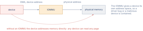
Figure 1 shows the path with and without one.
04.PCI Express
PCI Express is the dominant peripheral interconnect since 2004. It replaced the parallel PCI bus and the graphics-specific AGP slot with a serial point-to-point fabric.
The fundamental unit is a lane, a single differential pair in each direction. Lanes are clocked at multi-GHz rates determined by the PCIe generation. Each lane carries data using 8b/10b encoding (Gen1, Gen2), 128b/130b encoding (Gen3 through Gen5), or PAM4 signaling (Gen6 and later).
Table 2. PCIe generation bandwidth. Per-lane figures are the usable data rate after encoding overhead.
| Generation | Year | Per-lane (GB/s) | x16 link (GB/s) |
|---|---|---|---|
| PCIe 1.0 | 2003 | 0.25 | 4 |
| PCIe 2.0 | 2007 | 0.5 | 8 |
| PCIe 3.0 | 2010 | 1 | 16 |
| PCIe 4.0 | 2017 | 2 | 32 |
| PCIe 5.0 | 2019 | 4 | 64 |
| PCIe 6.0 | 2022 | 8 | 128 |
| PCIe 7.0 | 2025 (planned) | 16 | 256 |
A link aggregates multiple lanes between two endpoints: x1 (1 lane), x4, x8, x16. Each generation doubles the per-lane bandwidth, and a x16 link at PCIe 5 delivers 64 GB/s in each direction. This is a fraction of DRAM bandwidth but plenty for individual peripherals: a PCIe 5 x4 NVMe SSD does about 16 GB/s, a PCIe 5 x16 GPU about 64 GB/s.
PCIe is a switched fabric rather than a shared bus. The CPU’s root complex hosts a tree of PCIe links, with PCIe switches at the internal nodes and devices at the leaves. Each switch routes packets independently, so multiple devices can be communicating with the CPU simultaneously through separate switch ports. This contrasts with the old parallel PCI bus, where every device shared one set of wires and arbitrated for access.
The PCIe protocol stack has three layers.
Physical layer. Drives differential signaling on the lanes, performs clock recovery, equalization, and the encoding/decoding (8b/10b, 128b/130b, or PAM4). Handles link training: when a device is plugged in, the link partners negotiate the lane width and speed.
Data link layer. Wraps the TLPs (Transaction Layer Packets) handed down by the transaction layer with sequence numbers and CRCs, and generates acknowledgments. Handles retransmission of dropped or corrupted packets.
Transaction layer. Issues memory read, memory write, configuration read, configuration write, and message TLPs. This is the layer the CPU root complex and the device firmware interact with.
A memory read from the CPU to a device’s MMIO register becomes a non-posted read TLP that traverses the PCIe fabric to the device, which responds with a completion TLP carrying the data. A memory write to a device register becomes a posted write TLP, which the sender does not wait for an acknowledgment on. A DMA write from the device to host DRAM becomes a posted write TLP traversing the fabric in the opposite direction.
05.Address Translation Services
The IOMMU translation latency adds to every DMA. For a device that makes many small transfers (a NIC receiving small packets, a GPU fetching descriptors), the cumulative IOTLB miss cost can become significant. The Address Translation Services extension to PCIe [1] addresses this by letting the device cache translations locally.
The mechanism works as follows. Before issuing a DMA to address A, the device first issues a translation request for A. The IOMMU walks its page table, returns the translation along with the access permissions, and the device caches it in a local ATS cache (also called a device TLB). Subsequent DMAs to nearby pages can use the cached translation instead of going through the IOMMU.
The IOMMU and the OS coordinate on invalidations. When the OS unmaps a page, it must invalidate that page in every device that might have it cached, the same way the OS performs TLB shootdowns on CPU cores (see Chapter 42). The PCIe protocol provides the invalidation TLP for this purpose.
ATS is particularly important for accelerators with their own sophisticated memory hierarchies. An NVIDIA GPU with its own MMU, or an Intel DSA (Data Streaming Accelerator), or a SmartNIC with ARM cores running Linux, all benefit from caching translations locally rather than going to the host IOMMU on every memory reference.
06.Page Request Interface
A traditional DMA buffer must be pinned in host memory: the OS allocates a range of physical pages, ensures they are not swapped out, and gives the physical addresses to the device. This is fine for small buffers but limits flexibility for accelerators that want to access arbitrary parts of a user process’s virtual address space.
The Page Request Interface extension to PCIe allows a device to trigger an OS page-fault handler on a missing mapping, the same way a CPU does on a load to an unmapped page. The sequence is
-
The device attempts an access to an IOVA. The IOMMU walks the page table and finds an invalid entry.
-
Instead of failing the access immediately, the IOMMU signals the device with a translation completion that indicates "no mapping available, page request required".
-
The device sends a page request TLP to the IOMMU with the IOVA and the access type.
-
The IOMMU interrupts the OS, which runs its page fault handler. The handler may bring the page in from swap, allocate a fresh page, or fail the request.
-
Once the page is mapped, the IOMMU sends a page response TLP back to the device, which retries the access.
PRI lets accelerators share virtual memory with the CPU at the same granularity as a CPU thread, including demand paging. An NVIDIA GPU using Unified Memory or an Intel DSA using Shared Virtual Memory both rely on PRI to access user-process pages that may not be resident.
The cost of a page request is dominated by the OS interrupt handler, not the PRI protocol itself. A page request that finds the page already resident in DRAM (a soft fault) completes in roughly ten microseconds. A page request that requires reading from swap takes hundreds of microseconds. Devices with PRI-capable workloads need careful tuning to avoid spending more time waiting on page requests than doing useful computation.
For a soft fault, is roughly 5 to 10 us, and and are roughly 1 us each, totaling 7 to 12 us. For a hard fault that swaps in from NAND, rises to 100 us or more, dominated by the NAND read.
The combination of ATS, PRI, and the SVM model finally brings peripheral devices into the same virtual memory abstraction that CPU threads have used for decades. An accelerator can be programmed with pointers, walk linked lists, follow page-table-managed mappings, and share data structures with the host without the copy-on-DMA overhead of traditional driver models. This is a significant simplification for the software stack, paid for by the hardware complexity of ATS, PRI, and per-device IOMMU contexts.
07.Compute Express Link and the Future of I/O
PCIe is being extended by Compute Express Link (CXL), a protocol that runs on PCIe 5 and 6 physical links and multiplexes three sub-protocols on the link, two of which add transaction types beyond PCIe’s memory and configuration accesses.
CXL.io is essentially PCIe, used for device initialization and legacy traffic.
CXL.cache lets accelerators participate in the host’s cache coherence protocol. An accelerator can hold a cache line modified, the host can snoop it, the same as another CPU. This removes the round-trip to host DRAM for accelerator-host coherent accesses.
CXL.mem lets memory expansion modules attach over PCIe links and present their memory as part of the host’s coherent address space. A CXL-attached DRAM module appears as a NUMA node at higher latency than local DRAM but at the same coherent addressing. The mechanism enables memory pooling across servers and persistent memory expansion in DDR-form-factor modules.
CXL is the architectural endpoint of the trend this chapter has traced. Peripherals started outside the CPU’s memory model (separate I/O address space, no DMA, no IOMMU). They moved into the memory address space (MMIO, DMA). They moved into the virtual memory model (IOMMU, ATS, PRI). Now they move into the cache coherence model (CXL.cache) and the memory address space itself (CXL.mem). The boundary between CPU and accelerator continues to blur.
08.Worked Examples
09.Exercises
References
- [1](2024). “Intel.”