NVM, Storage, and Storage-Class Memory
September 8, 202623 min readadvanced
The memory hierarchy of Chapter 36 ends at DRAM, but the storage hierarchy continues below. Mass storage holds data when the power is off, with capacities orders of magnitude larger than DRAM at orders of…
The memory hierarchy of Chapter 36 ends at DRAM, but the storage hierarchy continues below. Mass storage holds data when the power is off, with capacities orders of magnitude larger than DRAM at orders of magnitude longer access times. For most of computing history, the gap between DRAM and storage was filled by rotating magnetic disks at 10 ms per access and 100 MB/s of bandwidth. This produced an obvious latency cliff: DRAM at 100 ns, disk at 10 ms, a ratio of 100,000. Caching DRAM contents was the only way to make the disk-backed working set tolerable.
Solid-state drives upended this picture in the 2010s by closing the DRAM-to-storage latency gap by two orders of magnitude. An NVMe SSD reads a 4 KiB page in 70 to 200 microseconds, 50 to 140 times faster than a spinning disk and 700 to 2000 times slower than DRAM. The hierarchy now has a three-tier shape: DRAM at sub-100 ns, SSD at tens to hundreds of microseconds, magnetic tape and archival storage at seconds or longer.
This chapter develops the storage tier from first principles. It starts with the NAND flash cell and the physics of charge trapping, walks through SLC through QLC encoding tradeoffs, covers 3D NAND’s vertical stacking, develops the NVMe SSD architecture and ZNS extension, traces the history of 3D XPoint and persistent memory, and closes with the persistence-ordering model that programmers must reason about when data outlives a power-cycle.
01.NAND Flash and Charge Trapping
A NAND flash cell is a single transistor whose threshold voltage () can be programmed by trapping charge in the gate stack. A high corresponds to one logical value, a low to the other. Reading the cell applies a fixed gate voltage and observes whether the transistor conducts. Programming injects electrons into the floating gate (or charge-trap layer) by hot-electron injection or Fowler-Nordheim tunneling, raising . Erasing extracts electrons by reverse Fowler-Nordheim tunneling, lowering to its default level.
The physics has two costs that the architecture has to accommodate.
Asymmetric write. Programming a cell raises , but the cell cannot be reprogrammed to a lower without first being erased. This means a write can only set bits to 0 in a fresh erase state, and lowering bits to the all-1 erase state requires erasing the entire block (typically several megabytes). A flash block is the unit of erase, a flash page (typically 16 KiB to 32 KiB) is the unit of program and read. A single block contains hundreds to thousands of pages.
Wear. Each program-erase cycle damages the gate oxide slightly, and after a few thousand to a few hundred thousand cycles the cell can no longer reliably distinguish program from erase states. SLC cells endure 100,000 cycles, MLC cells 10,000, TLC cells 3,000, and QLC cells 1,000 typically. The flash translation layer (FTL) inside the SSD remaps logical addresses to physical addresses to spread writes across all cells, so heavily-written logical addresses do not accumulate disproportionately on the same physical cells. This is wear leveling.
The combined effect is that a flash SSD looks like a block device to the host (with logical block addresses (LBAs), reads, writes, and TRIM commands), but internally maintains a substantial indirection layer. When a host writes LBA 12345 with new data, the FTL allocates a fresh physical page in some currently-erased block, writes the new data there, and updates the LBA-to-physical-page map. The old physical page is marked obsolete and will be reclaimed during the next garbage collection of its block.
02.SLC, MLC, TLC, QLC
A single NAND cell can store more than one bit by encoding multiple levels. Single-level cells (SLC) use two levels (low and high), storing 1 bit. Multi-level cells (MLC) use 4 levels for 2 bits. Triple-level cells (TLC) use 8 levels for 3 bits. Quad-level cells (QLC) use 16 levels for 4 bits. The density multiplier (vs SLC) is 1, 2, 3, 4 for the same number of cells.
The cost is signal margin. SLC has the full range (typically 3 to 5 volts) to distinguish its two states, giving large noise margin. QLC must distinguish 16 states in the same range, so each state has roughly 1/8 the margin. This affects three properties.
Bit error rate. QLC cells have much higher raw bit error rates than SLC. The SSD compensates with stronger error-correcting codes (LDPC at modern enterprise grade, BCH on older devices), adding latency but recovering correctness.
Endurance. Higher bit density also means each program-erase cycle has less margin to spare for oxide wear. An SLC cell can be cycled 100,000 times before its margin closes, while QLC can manage about 1,000.
Latency. Programming 16 levels requires multiple incremental-program-and-verify cycles to precisely place the charge, which makes QLC writes roughly 10 to 50 slower than SLC writes per bit. Reading is also slower, because the read circuit must perform multiple reference comparisons to identify which of 16 levels the cell holds.
Table 1. Per-cell properties of SLC through QLC NAND, drawn from public Samsung and Micron datasheets. Endurance is approximate program-erase cycles before bit error rate exceeds correctable levels.
| Cell type | Bits/cell | Endurance (P/E) | Write time (us) | Read time (us) |
|---|---|---|---|---|
| SLC | 1 | 100,000 | 30 to 50 | 25 to 40 |
| MLC | 2 | 10,000 | 200 to 800 | 50 to 100 |
| TLC | 3 | 3,000 | 700 to 3,000 | 60 to 150 |
| QLC | 4 | 1,000 | 1,500 to 7,000 | 80 to 250 |
The economics favor QLC for capacity-sensitive applications and SLC for write-heavy applications. Most consumer SSDs in 2024 are TLC with a portion of the cells operating as SLC cache (programmed with only 2 levels for incoming writes, then folded back into TLC during idle periods). The SLC cache hides the slow TLC write latency for bursts and keeps the underlying density high.
QLC has emerged for cold-storage tiers and some consumer devices where the write workload is light and the endurance is acceptable. Enterprise QLC SSDs target read-mostly archival workloads with 99 percent read and 1 percent write distributions. Penta-level cells (PLC, 5 bits per cell, 32 levels) are in research, but nobody has shipped them at volume because the signal margin closes below acceptable error rates for current process nodes.
03.3D NAND
Planar (2D) NAND ran out of room around the 14 nm process node. Cells became too small to hold enough charge, leakage between neighboring cells made multi-level encoding unreliable, and yield fell. The industry pivoted to 3D NAND: rather than shrinking the cell, stack many cell layers vertically and relax the per-cell area.
A 3D NAND chip looks like a forest of vertical pillars rising through stacked horizontal gate layers. Each pillar is a vertical string of cells, with the channel running through the center and the charge-trap region between the channel and the gate. Each horizontal layer in the stack is one cell in every vertical string, controlled by one shared word line. A current 232-layer 3D NAND chip has 232 cells per string, and millions of strings per chip.
The benefits of 3D NAND. First, density scales by adding layers rather than shrinking lateral geometry. Samsung’s V-NAND, Micron’s 3D NAND, SK Hynix’s 4D NAND, and Kioxia/WD’s BiCS Flash have all scaled to 200+ layers as of 2024, with roadmaps to 500+ layers by the late 2020s. Second, the per-cell geometry can be relaxed (70 nm or larger cell pitch is common), restoring the noise margin that planar scaling lost. Third, the charge-trap layer (used in charge-trap 3D NAND, as opposed to floating-gate) is more resilient to retention loss than a floating gate.
The costs of 3D NAND. First, the stacking process is hard. Etching uniform high-aspect-ratio holes through 232 layers of alternating oxide and conductor requires extreme process control. The yield falls with layer count, and the time per wafer rises. Second, the cells at the top and bottom of a tall string see different parasitic capacitances than those in the middle, so the SSD’s read and write circuits must compensate. Third, the strings are shared, so a single defect in a string can corrupt all 232 cells in it.
04.NVMe SSDs
An NVMe SSD is a NAND flash array, an SSD controller (an embedded ARM or RISC-V processor running the FTL), some DRAM for FTL metadata, and a PCIe interface. The host communicates with the SSD through the NVMe protocol, a queue-pair based command interface that replaced the older AHCI/SATA protocol designed for spinning disks.
The structural advantage of NVMe over AHCI is concurrency. AHCI supports one command queue with 32 outstanding commands. NVMe supports up to 64K queues each with 64K outstanding commands. A modern NVMe SSD typically uses 8 to 32 queues per host (one per CPU core), with hundreds of outstanding commands per queue. This matches the parallelism of the NAND array (multiple chips, multiple planes per chip, multiple LUNs) so that the host can saturate the SSD’s internal bandwidth.
A typical NVMe SSD has the following structure.
-
PCIe Gen4 x4 host interface (8 GB/s peak, 7.5 GB/s usable). Gen5 x4 doubles this to 16 GB/s peak.
-
SSD controller running the FTL (LBA translation, garbage collection, wear leveling, ECC).
-
DRAM (1 GB per 1 TB of NAND is a common ratio) holding the LBA mapping table and write-coalescing buffers.
-
NAND flash organized into channels (8 to 16 per controller), each with one or more chips, each with multiple planes.
The end-to-end latency of a 4 KiB read on a current NVMe SSD breaks down as
-
PCIe submission queue write and doorbell: 1 to 5 us.
-
Controller dispatch and FTL translation: 5 to 20 us.
-
NAND page read (TLC, 16 KiB page servicing the 4 KiB request): 60 to 150 us.
-
ECC decode and data transfer back over PCIe: 5 to 20 us.
Total: 70 to 200 us for a single random read. Sequential streaming reads pipeline these stages and approach the PCIe bandwidth limit. Write latency is dominated by the FTL’s metadata update and the slow programming of the cells, typically 200 to 1000 us for a small write.
The SSD’s behavior under sustained write load is shaped by garbage collection. The FTL allocates pages from freshly-erased blocks. When free blocks run short, it must select blocks with mostly-obsolete pages, copy the remaining valid pages to a new block, and erase the source. This copy traffic is called write amplification. An SSD with WAF = 2 means every host write causes 2 physical writes inside the SSD (1 from the host plus 1 from garbage collection), halving effective endurance and bandwidth. Steady-state WAF on a heavily-utilized SSD can be 3 to 10 depending on workload.
05.Zoned Namespace SSDs
The FTL exists to hide NAND’s erase-block-aligned constraint from the host. This is fine for general-purpose use but adds overhead for workloads that already have erase-block-aligned access patterns (databases with log-structured storage, large object stores, video recording). These workloads internally use append-only data structures that naturally produce sequential writes within controllable units, but the FTL between them and the NAND reintroduces random-access semantics and the associated garbage collection.
Zoned Namespace SSDs (ZNS) expose the NAND directly as a collection of zones, each one or more erase blocks large, each accepting only append writes. The host explicitly allocates a zone, writes to it sequentially, optionally resets (erases) it when done, and moves on. There is no FTL garbage collection, no write amplification beyond what the host introduces, and no DRAM mapping table for indirection. The SSD controller becomes much simpler.
The cost is that the host must implement the layout that the FTL formerly hid. A ZNS SSD is unusable as a general-purpose disk by most file systems. Linux has added zoned-storage support for Btrfs, F2FS, and certain database engines (RocksDB, MariaDB). Cloud storage vendors deploy ZNS at scale because their software stacks already match the zoned model.
ZNS is one example of a broader trend in storage architecture: move complexity from the SSD controller back into the host stack where the workload-specific knowledge lives. Similar ideas appear in NVMe Open-Channel SSDs (host manages logical-to-physical mapping), Computational Storage (the SSD runs user-supplied functions near the NAND), and the various forms of host-managed SMR (shingled magnetic recording) drives.
06.3D XPoint and the Memory-Storage Gap
Between DRAM (sub-100 ns, \5$0.10$ per GB, non-volatile, block addressable) sits a gap of three orders of magnitude in latency and two in cost. Filling this gap with a single device has been a research goal for decades. Several candidates emerged in the 2010s: phase-change memory (PCM), magnetoresistive RAM (MRAM), resistive RAM (ReRAM), ferroelectric RAM (FRAM). Each shipped at small scale. The most aggressive deployment came from Intel and Micron with 3D XPoint.
3D XPoint, marketed by Intel as Optane, is a crosspoint memory technology with a chalcogenide-based selector and storage layer. The cells are accessed by selecting a single row and column from a crossing-bar array, with no transistor per cell. The technology shipped in two product lines from 2017 to 2022.
Optane SSDs. PCIe-attached drives that competed with NAND SSDs at the high end. Read latency was 10 us, an order of magnitude faster than the best NAND. Bandwidth was 2.5 GB/s. Endurance was 60 drive writes per day, vs 1 to 3 for enterprise NAND. The products were popular in finance and database tiers but expensive.
Optane DC Persistent Memory. DDR4-form-factor modules that plugged into a DIMM slot and were accessed through CPU load and store instructions as persistent memory (PMEM). Latency was 100 to 300 ns for reads (vs 80 ns for DRAM), 1 us or so for writes. Capacity was up to 512 GB per module, much larger than DRAM modules. The data persisted across power cycles.
3D XPoint did not survive the commercial environment. Intel ended manufacturing in 2022, citing insufficient demand to offset manufacturing complexity. The technology was real, the latency gap was real, and the data-center workloads that benefited (large in-memory databases, high-tail-latency-sensitive caches) were also real. But the market did not develop fast enough to justify the capital expenditure, and DRAM density continued to improve while NAND density caught up on bandwidth. The gap closed from both sides.
The lessons from 3D XPoint persist. The CXL ecosystem and the recent push for byte-addressable persistent memory in the CXL.mem specification incorporate the persistent-memory programming model that Optane introduced. Future memory technologies (MRAM in embedded products, ReRAM in neuromorphic accelerators) build on the software abstractions that Optane required.
Table 2. Approximate latency and cost across the memory-storage hierarchy as of 2024. Costs are per GB at retail, which substantially overstates true component cost at hyperscale volumes.
| Technology | Latency | Bandwidth | Cost ($/GB) |
|---|---|---|---|
| SRAM (L1 cache) | 1 ns | 1000s GB/s | 100 to 1000 |
| DRAM (DDR5) | 80 ns | 50 GB/s/ch | 5 to 10 |
| 3D XPoint (Optane PMEM) | 200 ns | 8 GB/s/module | 8 to 12 |
| NVMe SSD (TLC) | 100 us | 7 GB/s | 0.10 |
| NVMe SSD (QLC) | 200 us | 6 GB/s | 0.05 |
| Magnetic disk (HDD) | 10 ms | 0.2 GB/s | 0.02 |
| Tape (LTO-9) | seconds | 0.4 GB/s | 0.005 |
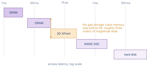
Figure 1 shows the hole in the latency ladder.
07.Persistent Memory and Persistence Ordering
When NVM is accessed through CPU load and store instructions (rather than through a block-storage stack), the programming model diverges from both DRAM and traditional storage. Two issues dominate.
Atomicity. A traditional file-system write is atomic at the file-system block granularity: either the block is fully written or it is not. A PMEM store may be in flight at the moment of a power loss, leaving the cache line half-written. The processor’s store buffer, the L1 cache, the L2 and L3 caches, the memory controller’s write queue, and the DIMM’s internal buffer all hold data that has not yet been committed to the NVM array. A crash anywhere in this pipeline can leave inconsistent state.
Ordering. A program that updates a data structure typically performs a sequence of stores that need to commit to persistent storage in a particular order. Suppose the program appends a node to a linked list by writing the new node’s data, then writing a pointer from the previous tail to the new node. If the cache evicts the pointer before evicting the new node’s data, a crash leaves a list whose tail points at an uninitialized node. This is a violation of the program’s intended persistence order.
Intel’s solution introduced new instructions for explicit cache line writeback to NVM: CLWB (cache line write back, leaves the line in cache) and CLFLUSHOPT (cache line flush optimized, evicts the line). After a sequence of CLWB instructions, the program issues SFENCE to wait for them to drain. This sequence is the persistent-memory equivalent of fsync on a file system, but at cache-line granularity and without an OS call.
Idealized persistent linked-list append with cache flushes.
typedef struct node {
    struct node *next;
    int data;
} node_t;

void append(node_t *tail, int value) {
    node_t *n = pmem_alloc(sizeof *n);
    n->next = NULL;
    n->data = value;

    /* Make sure new node's contents are persistent before
    * tail->next pointer becomes visible. */
    clwb(&n->next);
    clwb(&n->data);
    sfence();

    tail->next = n;
    clwb(&tail->next);
    sfence();
}
The two SFENCE calls enforce ordering. Without them, the hardware is free to commit tail->next before n->data reaches NVM, breaking the invariant on a crash.
The complexity of persistent-memory programming is one reason 3D XPoint did not take off. Application programmers were unwilling to rewrite data structures around CLWB and SFENCE, file system developers had little incentive to expose PMEM semantics, and the use cases that benefited (in-memory database checkpointing, high-frequency-trading state journaling) were narrow. The PMEM programming model survives in the CXL.mem specification and in software libraries like PMDK (Persistent Memory Development Kit), now maintained by the broader community after Intel’s exit from the product line.
08.Why SSDs Are Not RAM
The convergence of NAND latency toward DRAM has invited the question: can SSDs eventually replace DRAM? The answer is no, for several structural reasons that this chapter has touched on.
Latency floor. NAND read latency is bounded below by the analog sensing of the floating gate state, which must settle the bit line and compare it against one or more reference levels. Even SLC at the fastest process is 25 to 40 us per page read. That is two orders of magnitude slower than DRAM and likely to remain so.
Granularity. NAND is read at the page granularity (16 to 32 KiB) and written at the same granularity. DRAM is accessed at the byte (or cache-line, 64-byte) granularity. Treating an SSD as RAM would amplify bandwidth requirements by 256 to 512 for random small accesses.
Write asymmetry. NAND cannot write in place. Updating a single byte at LBA 12345 requires reading the containing page, modifying it, and writing the page to a freshly-erased block, with the FTL updating mapping metadata. This is many orders of magnitude slower than the DRAM write it would replace.
Endurance. NAND cells wear out. A workload that touches DRAM at the full bandwidth (50 GB/s) would exhaust QLC NAND endurance in days. Even SLC NAND would last only months at DRAM bandwidth.
Power. NAND depends on on-chip charge pumps for its word line voltages, at 15 to 20 V for program and erase and at a pass voltage well above on the unselected word lines during a read. Driving those pumps and the sense amplifiers dissipates milliwatts per read. DRAM reads dissipate microwatts. Replacing DRAM with NAND at the same access rate would multiply memory power by orders of magnitude.
The right way to think about SSDs is as the fastest tier of storage rather than the slowest tier of memory. The DRAM-SSD gap will continue to exist as long as the underlying physics of charge trapping and capacitor refresh remain different. Storage-class memory technologies that genuinely close the gap (MRAM at modest capacity, future PCM variants, CXL-attached NVDIMMs) occupy a distinct architectural tier rather than replacing DRAM or SSDs.