Digital Logic, Timing, and Sequential Fundamentals
September 8, 202628 min readadvanced
Start below the logic. A MOSFET transistor has three terminals that matter, the gate, the source, and the drain. Put a voltage on the gate and current can flow between source and drain. Remove it and current…
01.Part 1, from a switch to a gate
1.1 The transistor is a switch
Start below the logic. A MOSFET transistor has three terminals that matter, the gate, the source, and the drain. Put a voltage on the gate and current can flow between source and drain. Remove it and current cannot. That is all it does for our purposes. It is a switch whose control input is a voltage rather than a finger.
There are two flavors. An NMOS transistor conducts when its gate is high. A PMOS transistor conducts when its gate is low. They are opposites, and that opposition is what makes CMOS work.
CMOS stands for complementary MOS, and the word complementary is the whole idea. Every gate is built from two networks. A pull-up network of PMOS transistors that connects the output to the supply voltage, and a pull-down network of NMOS transistors that connects the output to ground. They are wired so that exactly one is conducting at any time.
Look at the simplest possible example, an inverter.
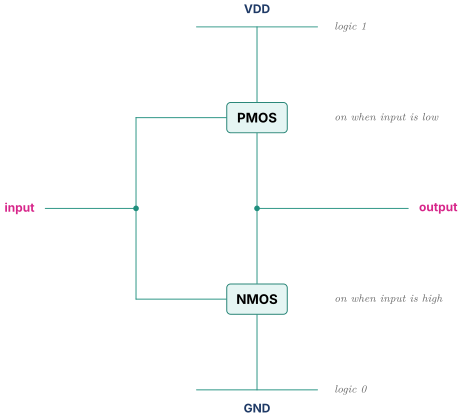
Feed in a low input. The PMOS conducts, the NMOS does not, so the output connects to VDD and reads high. Feed in a high input. The PMOS shuts off, the NMOS conducts, so the output connects to ground and reads low. Input low gives output high and input high gives output low, which is exactly an inverter.
Notice something important. In both steady states there is no path from VDD to ground, because exactly one network conducts. So a CMOS gate that is sitting still draws essentially no current. That single property is why CMOS beat every competing logic family and why chips can have billions of gates without melting. It also sets up the power discussion in Power Fundamentals and Clock Gating, where you will see that CMOS burns power only when it switches.
1.2 Where delay actually comes from
Now the fact that everything else in this note depends on. A gate does not respond instantly.
The reason is physical and worth understanding rather than memorizing. The output of a gate is a wire connected to the inputs of other gates. That wire and those inputs together form a capacitance, meaning they store charge. To change the output from low to high, the transistors must physically move charge onto that capacitance. To change it from high to low, they must drain that charge away.
Moving charge takes time, and how much time depends on two things. How much charge is needed, which is the capacitance , and how fast the transistor can supply it, which is the current . Roughly,
Three consequences follow immediately, and each of them shows up repeatedly in later notes.
Driving more gates is slower. More inputs connected to your output means more capacitance, so the same transistor takes longer. This is fanout, and it is why a signal feeding a thousand places needs a tree of buffers rather than one driver.
Longer wires are slower. A long wire has more capacitance than a short one. This is why physical placement affects timing, why STA Synthesis and Physical Design cares about congestion, and why Execution Units talks about clustering.
Bigger transistors are faster but cost more. A wider transistor supplies more current, so it charges the capacitance faster, at the cost of area and of presenting more capacitance to whatever drives it. Synthesis tools spend most of their effort on exactly this trade, which is cell sizing.
Use a round number throughout this note. One gate takes 1 nanosecond, written 1 ns, which is seconds. Real gates in a modern process are far faster, more like 5 to 20 picoseconds, but 1 ns keeps the arithmetic doable in your head and none of the reasoning changes.
02.Part 2, why glitches happen
2.1 Build a small adder
A full adder takes three inputs, two bits to add plus a carry coming in, and produces two outputs, a sum bit and a carry going out. It is the basic unit of binary addition, and it works exactly like adding a column in grade-school arithmetic, where you write down a digit and carry one to the next column.
Chain four of them to add two 4-bit numbers. The carry out of each stage becomes the carry in of the next, which is why this is called a ripple-carry adder. The carry ripples upward like a rumor passing down a line of people.
Assume each full adder takes 2 ns to produce its outputs after its inputs are stable.
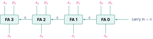
Read the arrows carefully. Stage 0 can start immediately because its carry in is known. Stage 1 cannot finish until stage 0 gives it a carry. Stage 2 waits on stage 1. Stage 3 waits on stage 2. They are not independent, they are a chain.
2.2 Watch it compute 7 plus 1
Feed in , which is 7, and , which is 1. The correct answer is , which is 8.
Before this input arrives, suppose the adder had been showing from a previous calculation. Now trace what the output pins physically show as time passes.
At , the inputs change. Nothing has propagated yet, so the outputs still show the old value, .
At ns, stage 0 finishes. It computed in binary, so and it sends a carry to stage 1. Only bit 0 has updated, so the output now reads . But stages 1, 2, and 3 are still showing their old values because the carry has not reached them.
At ns, stage 1 finishes. It received the carry and computed , so and it passes a carry up. Output reads .
At ns, stage 2 finishes the same way. , carry up. Output reads .
At ns, stage 3 finally receives the carry and computes , so . Output reads , which is 8. Correct at last.
Collected into a table.
| Time | What just settled | Output bits | Reads as |
|---|---|---|---|
| nothing, old value | 7 | ||
| ns | stage 0 | 6 | |
| ns | stage 1 | 4 | |
| ns | stage 2 | 0 | |
| ns | stage 3 | 8, correct |
2.3 Sit with what that table says
Between and ns, the adder output showed 7, then 6, then 4, then zero, and only then 8.
It displayed zero. Not as a fault, not as an error condition. Every transistor in that adder is working perfectly. Those intermediate values are simply the carry making its way up the chain, one stage at a time, with each stage faithfully showing its old result until new information arrives.
Those transient wrong values have a name. They are glitches, and here is the key fact. Every real combinational circuit produces them. This is not a defect to be engineered away, it is a consequence of information taking time to travel. Any circuit whose output depends on several inputs arriving through paths of different lengths will show wrong values in between.
2.4 The critical path
Suppose some other part of the chip had looked at that adder's output at ns. It would have read 4, and it would have believed it, and nothing anywhere would have flagged the value as wrong.
So the output of a block of logic is trustworthy only after enough time has passed for the longest path through it to settle. Here that is 8 ns, the full carry chain from bit 0 up to bit 3.
That longest path is the critical path, and the time it takes is the propagation delay of the block. You will hear both terms constantly for the rest of your career, and this is all they mean. The slowest route from any input to any output.
Notice that "longest" means slowest in time, not longest in physical distance or in number of gates, though those usually correlate. A path through four slow gates can beat a path through six fast ones.
03.Part 3, the clock
3.1 The problem stated plainly
You now have a real difficulty. The logic gives the right answer eventually but lies in the meantime, and nothing about the output itself tells you which regime you are in. Something must decide when eventually has arrived.
There are exactly two ways to solve this, and it is worth seeing both to understand why the industry picked one.
Way one, ask. Have the logic signal when it is finished, and have the consumer acknowledge receipt. This is asynchronous design. It genuinely works, and it has real advantages, since a block that finishes early does not have to wait. The problem is cost. Every block needs completion-detection circuitry, which is often as large as the logic itself, plus handshaking wires everywhere. Worse, analyzing whether such a system is correct and fast is extremely hard, because there is no common time reference to reason against. Almost nobody builds large chips this way.
Way two, agree in advance. Pick a time interval long enough that the slowest path in the whole design has certainly settled. Have everybody look at everything only at interval boundaries. Nobody needs to ask anyone anything. Everybody just needs a shared signal announcing when a boundary occurs.
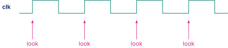
That shared signal is the clock. It is not mysterious. It is a square wave that alternates high and low at a fixed rate, and its rising edges are the moments everyone has agreed to look.
3.2 The trade that defines the field
If the adder needs 8 ns, the clock period must be at least 8 ns, so the frequency can be at most
Now generalize that, because it is the single most important trade in digital design.
The clock frequency of a chip is set by the slowest path anywhere in it.
Read that again. Not the average path. Not most paths. The slowest single path. If a design has ten million paths and 9,999,999 of them settle in 0.3 ns while one takes 0.5 ns, the whole chip runs at the speed the 0.5 ns path allows. Everything else waits.
That asymmetry is why hardware engineers spend so much of their working life hunting critical paths, and why the timing reports in STA Synthesis and Physical Design are sorted worst-first. Fixing the worst path is the only thing that helps, until it stops being the worst path and something else becomes the limiter.
04.Part 4, the device that captures
4.1 What a flip-flop does
Agreeing on a moment is useless unless something actually captures the value at that moment and holds it steady until the next one. That device is the flip-flop.
A D flip-flop has a data input called , a clock input, and an output called . Its entire behavior is one sentence.
At the rising edge of the clock, copy whatever is on to , and hold that value until the next rising edge.
That is it. Between edges, may do absolutely anything. It may glitch through 7, 6, 4, and 0 exactly as the adder did. The flip-flop does not care, because it is not looking. It looks only at the edge.
This is the mechanism that makes the whole scheme work, and it is worth stating as a principle. A flip-flop converts a signal that is only sometimes correct into a signal that is always correct, by sampling it at a moment when correctness is guaranteed.
4.2 Latches, and the difference that gets asked
A latch is the flip-flop's close relative and the distinction comes up in interviews constantly.
A latch is level-sensitive rather than edge-sensitive. While the clock is high, a latch is transparent, meaning simply follows continuously, glitches and all. When the clock falls, the latch closes and freezes whatever value was there.
Put them side by side.
| Latch | Flip-flop | |
|---|---|---|
| Sensitive to | clock level | clock edge |
| Open for | half a cycle | an instant |
| Passes glitches | yes, while open | no |
| Area and power | smaller, cheaper | larger |
| Timing analysis | harder | easier |
In fact a flip-flop is usually built from two latches wired back to back with opposite clock polarity, so that only one is ever open. The first captures while the clock is low, the second passes the value out when the clock goes high, and at no point is there a straight path from to . This is called a master-slave arrangement, and it is why a flip-flop costs roughly twice a latch.
Why anyone uses latches. Because being transparent for a window lets timing slack move between pipeline stages. If one stage finishes early and the next is slow, a latch lets the slow stage start early and effectively borrow time. This is time borrowing, and it is genuinely valuable in high-performance datapaths where every picosecond matters. The cost is a much harder timing and verification problem, which is why latches appear in places like high-end CPU datapaths and rarely elsewhere.
Latches also appear inside clock gating cells for a reason explained fully in Power Fundamentals and Clock Gating, and that is the most likely place you will meet one deliberately.
4.3 The definitions, now that you have seen them
Only now do the textbook definitions carry meaning.
Combinational logic has outputs that depend only on its present inputs. Our adder is combinational. Give it 7 and 1, wait long enough, and you get 8, no matter what it was doing a moment before. It has no memory. In hardware it is gates with no feedback and no storage elements.
Sequential logic has outputs that depend on present inputs and on stored state. A flip-flop is the simplest sequential element. A counter is sequential, because what it outputs next depends on what it is holding now.
Real designs are built by alternating the two.

Flops hold the current state. Combinational logic reads that state, computes, and glitches its way toward an answer. At the next clock edge another bank of flops captures the settled answer. Repeat forever.
That alternating structure is the synchronous design discipline, and essentially every chip you have ever used is built this way, including every processor in every Apple product.
05.Part 5, setup and hold
5.1 Why a flip-flop needs margin
So far the flip-flop sampled "at the edge," as though the edge were a mathematical instant of zero width. Real flip-flops are not instants.
Recall from 4.2 that a flip-flop is built from latches, which are built from cross-coupled gates. To reliably capture a value, that internal circuit needs a moment to make up its mind, and it needs the input to stay still while it does. Imagine trying to photograph a written number, you need the paper held steady for the duration of the exposure, both a little before and a little after you press the button.
That produces two requirements. Both are properties of the flip-flop cell itself, measured by the foundry and written into the cell library that synthesis reads.
Setup time, written , is how long the data must already be stable before the clock edge arrives.
Hold time, written , is how long the data must remain stable after the clock edge has arrived.
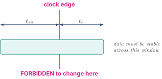
Together they define a small forbidden window straddling the edge. If the data changes inside that window, the flip-flop is not guaranteed to capture either the old value or the new one. It may do something considerably worse, which is the subject of Clocking Reset and Domain Crossing.
5.2 The circuit every timing question is about
Nearly every timing question you will ever be asked reduces to one picture. Two flip-flops with combinational logic between them, both fed by the same clock.
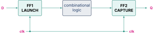
FF1 is the launch flop. On a clock edge it releases a value. That value travels through the logic, glitching along the way exactly as the adder did. FF2 is the capture flop. On the next clock edge it grabs whatever has arrived.
Two separate questions must both be answered yes, and confusing them is the most common mistake in this whole area.
Does the data get there in time? That is setup. Does the data stay put long enough? That is hold.
5.3 Setup, worked with numbers
Setup asks whether the data arrives early enough.
Follow the journey. The data leaves FF1 some time after the launch edge, and that delay is the clock-to-Q time, written , which is how long the flop takes to actually drive its output after being clocked. Then the data crosses the combinational logic, taking up to . Then it must land at FF2 and sit still for before the next clock edge, which arrives one period later.
Add up the journey and require it to fit inside one period.
Now put real numbers on it. Take a 100 MHz clock, so ns, and
- ns
- ns
- ns
The journey needs ns. The clock gives it 10 ns. It fits, with 2 ns to spare.
That spare time is called slack, and it is simply what you had minus what you needed.
Positive slack passes. Negative slack fails. When an engineer says a path "has negative slack" or the design "fails timing by 200 picoseconds," this is the number being quoted.
5.4 Break it on purpose
Now speed the clock up and watch it fail, because seeing the failure is more instructive than seeing the pass.
At 125 MHz, ns. Slack is . The design works in theory and has zero margin, which in practice means it does not work, because temperature, voltage, and manufacturing variation will eat any design with no margin.
At 143 MHz, ns.
The data is arriving 1 ns too late. At the capture edge, FF2 grabs whatever happens to be on its input at that moment, which is a half-finished glitch value, exactly like reading the adder at ns and getting 4.
This is a setup violation, and it is the reason every chip has a maximum frequency printed on it. Push past it and the chip computes wrong answers.
Notice what the equation is telling you. Setup is a race between the data path and the clock period. Anything that lengthens the data path hurts. Anything that lengthens the period helps.
5.5 Hold, which is genuinely different
Hold asks something that sounds similar and is not, and this is the part people get wrong.
Hold is not about the next clock edge. It is about the same clock edge.
Here is the situation. At the launch edge, FF1 releases new data, which races through the logic toward FF2. But FF2 is being clocked by that very same edge, and at that instant FF2 is still busy capturing the previous value. If the new data arrives too quickly, it corrupts the capture that is currently in progress.
So the requirement is that new data must not arrive until FF2 has finished, which takes after the edge.
Two details matter here and both trip people up.
First, this uses minimum delays, not maximum. Setup worries about the slowest path because that is what might arrive too late. Hold worries about the fastest path because that is what might arrive too early. They are genuinely different paths through the same logic.
Second, does not appear anywhere in this equation. Hold the thought, it is the punchline of the next section.
Numbers. Suppose ns, ns, and ns. The earliest new data can arrive is ns after the edge, and FF2 needs 0.3 ns. It passes, with 0.3 ns of hold slack.
Now a dangerous case. Consider a flop wired directly to another flop with no logic at all, so . In a library where ns and ns,
Hold violation. The new value arrives 0.1 ns too early and destroys the capture. And note that this happened with no logic between the flops at all, which is a configuration that looks completely innocent in RTL.
5.6 The punchline
Put the two equations side by side and look for what is missing.
The clock period appears in the setup equation and is completely absent from the hold equation.
That single observation has a consequence you will be asked about directly, probably in your first technical screen.
You cannot fix a hold violation by slowing down the clock.
Slowing the clock makes larger. That helps setup enormously and does absolutely nothing for hold, because hold never depended on in the first place. Hold is a race that happens entirely within a single clock edge, so stretching the gap between edges is irrelevant.
The reason this is such a good interview question is that people who memorized the equations get it wrong and people who understood the mechanism get it right. If you remember that hold is a race within one edge while setup is a race between two edges, you will never get it wrong.
A second consequence follows and is worth carrying.
A setup violation is a performance problem. The chip works, just not that fast. You can ship it at a lower frequency and sell it as a slower part. Manufacturers do this routinely, which is where speed grades come from.
A hold violation is a functional problem. The chip is broken at every frequency, including very slow ones, because the race does not depend on frequency. You cannot ship it at all. The silicon is scrap.
That is why hold violations escaping to silicon are treated as far more serious, and why the flow spends so much effort on them.
06.Part 6, clock skew and jitter
6.1 The clock does not arrive everywhere at once
So far both flip-flops received the clock edge at the same instant. Real chips are not like that.
The clock comes from one source and must reach hundreds of thousands of flops spread across millimetres of silicon. It travels through a tree of buffers and wires, and different branches have different delays. The difference in arrival time between two specific flops is clock skew.
Define the skew as how much later the clock reaches the capture flop FF2 than the launch flop FF1. Positive means FF2's edge comes later.
Now redo both equations. If FF2's edge arrives later, then FF2's capture happens at rather than , so the data has extra time.
6.2 Skew helps one and hurts the other
Read those two equations and notice that moved to the helpful side in setup and to the harmful side in hold. That is not a coincidence, it is the same physical fact seen twice.
If FF2's capture edge is later, the data has longer to arrive, which helps setup. But the new data is still launching at the same early time, and now FF2's capture window has moved later toward it, which hurts hold.
Work it through with ns on the earlier numbers.
Setup needed 8 ns and now has , so the design closes at ns instead of 8 ns. Skew just bought you frequency, from 125 MHz to 133 MHz.
Hold needed and now needs . That fails. The exact same skew that helped setup just created a hold violation.
This tension is why clock tree design is a specialty of its own, covered in Clocking Reset and Domain Crossing. Deliberately introducing skew to help a critical path is a real technique called useful skew, and every picosecond of it is borrowed against hold margin somewhere else.
6.3 Jitter is a different thing
Skew is a difference in space, the arrival time at point A versus point B, and it is roughly constant cycle to cycle because it comes from fixed wire and buffer delays.
Jitter is a difference in time, the arrival at one point on this cycle versus the next, caused by noise, supply variation, and the oscillator itself. It changes every cycle and is unpredictable.
Because jitter is unpredictable, it is treated as uncertainty and charged against setup margin. If the edge might arrive 50 ps early on any given cycle, you must design as though it always does.
07.Part 7, fixing violations
7.1 Fixing setup
For a setup violation you either shorten the data path or lengthen the period. In rough order of preference.
Restructure the logic to reduce depth. This is the most effective lever and it is an RTL change. Replace a long chain of operations with a tree, precompute something a cycle earlier, or simplify the function. A designer who can do this is worth a great deal.
Add a pipeline stage. Split the logic in two with a new flop bank in the middle, so each half has a full period. This raises frequency and adds a cycle of latency, and may require changes elsewhere to tolerate that.
Resize and buffer. Synthesis upsizes cells on the critical path so they drive their capacitance faster, and inserts buffers on long nets. The tool does this automatically.
Improve placement so the wires on that path are shorter, which reduces capacitance and therefore delay.
Apply useful skew, borrowing time as in 6.2, at the cost of hold margin.
Lower the frequency. The last resort, and a product decision rather than an engineering one.
7.2 Fixing hold
For hold you must lengthen the short path, because is unavailable to you.
Insert delay. Add buffers or dedicated delay cells on the data path so the new value arrives later. This is the standard fix and place-and-route tools do it automatically, late in the flow.
Use slower cells. Swap in higher-threshold or smaller cells on that path, which are slower and also leak less.
Fix the clock tree so the skew stops working against you.
Note the asymmetry in cost. Setup fixes generally buy you performance. Hold fixes cost area and power and buy you nothing except correctness, because you are deliberately adding delay to a path that was already fast enough. That is why designers try not to create hold problems in the first place, and why careless use of useful skew or clock gating is expensive.
08.Part 9, check yourself
Answer out loud, in full sentences, as if an interviewer asked. If you cannot, reread the section named.
- Why does a CMOS gate draw almost no current when it is sitting still, and what does that imply about when it does draw current? (1.1)
- Where does gate delay physically come from? Name three design consequences. (1.2)
- A combinational block briefly outputs a value that is not the correct answer. Is this a bug? Explain the mechanism. (2.3)
- Define critical path. Why does one slow path limit the entire chip? (2.4, 3.2)
- Why did the industry choose synchronous over asynchronous design? (3.1)
- Why does a flip-flop not care that its input glitched? (4.1)
- Compare a latch and a flip-flop. Why would anyone accept a latch's extra difficulty? (4.2)
- Write both timing equations from memory. Point at which term is the longest path and which is the shortest, and explain why they are different paths. (5.3, 5.5)
- Your chip fails hold at 2 GHz. A colleague suggests shipping at 1 GHz. What do you tell them and why? (5.6)
- Why is a setup violation a performance problem while a hold violation is a functional one? (5.6)
- A design has +2 ns setup slack and +0.05 ns hold slack. Which worries you more? (5.6, 7.2)
- Explain how adding clock skew can fix a setup violation, and what it costs you. (6.2)
- Distinguish skew from jitter. Why is jitter charged against setup margin? (6.3)
- You add a buffer to a data path. What happens to setup slack and to hold slack on that path? (7.1, 7.2)
- Why do hold fixes cost area and power while buying no performance? (7.2)
09.Part 10, related notes
- Clocking Reset and Domain Crossing for what happens when the two flops are on different clocks, where the forbidden window is violated with certainty
- Power Fundamentals and Clock Gating for why gating exists and what it does to the clock tree
- STA Synthesis and Physical Design for how these two equations become an industrial signoff process
- Arbiters FIFOs and CAMs for the first structures built from this foundation
- Sequential Logic and Timing for the vault's deeper treatment including register files and counters