Clock Generation, Distribution, Reset, and Domain Crossing
September 8, 202642 min readadvanced
A quartz crystal is the opposite. Its frequency comes from the mechanical resonance of a physical slab, and dimensions barely move with temperature or voltage, so a 24 MHz part good to 20 parts per million…
01.Part 1, where a clock comes from
1.1 Why you cannot just build an oscillator
The obvious way to make a clock is a ring oscillator, an odd number of inverters wired in a loop so the signal chases its own tail. With 11 stages at 20 ps each, a transition goes around twice per full period, so ps and GHz. Now heat the chip. Transistors slow down, each inverter takes 28 ps, so ps and GHz. The frequency dropped 29 percent because the chip got warm. Voltage droop and process variation move it again. A ring oscillator is a thermometer, not a time reference, and real chips use them as exactly that.
A quartz crystal is the opposite. Its frequency comes from the mechanical resonance of a physical slab, and dimensions barely move with temperature or voltage, so a 24 MHz part good to 20 parts per million stays within 480 Hz of nominal forever. But higher frequency means a thinner slab, and fundamental-mode crystals stop around 100 to 200 MHz. You cannot buy a 3 GHz crystal. So you have an accurate slow reference, you need a fast clock, and something must multiply frequency without losing accuracy.
1.2 The PLL, built one block at a time
Derive it rather than memorizing it, because each block fixes a problem the previous one created.
A controllable oscillator. Let a control voltage set how much current the ring's inverters get. That is a voltage-controlled oscillator. Say it gives 2.9 GHz at 0.50 V and 3.1 GHz at 0.60 V, so GHz per volt and you want 0.55 V. That voltage drifts, so open loop this is no better than before.
A way to compare. You cannot compare 3 GHz against 24 MHz. A feedback divider counting to turns 3 GHz into 24 MHz, which is comparable.
A comparator. A phase detector emits an UP pulse when the feedback edge is late and a DOWN pulse when it is early, with width equal to the error.
Something that remembers. A charge pump turns UP into current pushed onto a capacitor and DOWN into current pulled off, and the loop filter smooths those pulses into a slowly moving control voltage.
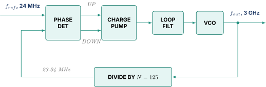
Trace it. A VCO at 2.88 GHz gives feedback at MHz, slower than the reference, so the feedback edge falls further behind each cycle and UP pulses grow. The charge pump raises the control voltage, the VCO speeds up, the pulses shrink, and at 24.00 MHz they vanish. The loop is locked.
1.3 The one equation
At lock the divided feedback equals the reference, so
The output is an integer multiple of a quartz-accurate reference, inheriting the accuracy while running 125 times faster. Change and you change frequency, which is the hook DVFS uses in DVFS Droop and Thermal. With MHz, gives 1.80 GHz, gives 2.40 GHz, gives 3.00 GHz, and gives 3.60 GHz.
Granularity is itself, so 3.01 GHz is unavailable. A reference divider ahead of the phase detector gives , so makes the step 6 MHz and still lands on 3.00 GHz, at the cost of jitter because a slower phase-detector rate corrects less often. There is also usually a post-divider after the VCO and outside the loop, so a fixed 3 GHz VCO yields 3 GHz, 1.5 GHz, 750 MHz, or 375 MHz. Remember that, it answers the next section.
1.4 Relock latency
A loop with an integrator does not respond instantly. Change and the control voltage must slew, overshoot, ring, and settle, which takes 20 to 100 microseconds. At 3 GHz a 50 µs relock is cycles of clock you cannot use. So real designs almost never relock to change frequency. They switch the post-divider, which takes a handful of cycles and gives integer fractions of the top frequency, or they switch to a second PLL already locked at the target. Both end in the same place. Something must swap one running clock for another, which is 2.5.
1.5 Jitter, priced in picoseconds
Jitter is cycle-to-cycle variation in edge position, and a PLL manufactures it in bulk because it is a loop that is always correcting. VCO phase noise, charge-pump current mismatch, and supply noise into the VCO all land as edges in the wrong place. Price it at 3 GHz where ps, since clock uncertainty comes straight out of the setup budget.
With ps, ps, jitter 15 ps, and skew 20 ps, the logic gets ps instead of 283 ps. You gave away 35 ps, which is 12 percent of the logic budget, or about two gate delays out of every path in the design.
1.6 The DLL, a different machine
A delay-locked loop has no oscillator, only a chain of controlled delay elements, and the loop adjusts total delay so the output edge lands where you want it. Input edges pass through rather than being regenerated. That one structural difference produces every behavioral difference.
| PLL | DLL | |
|---|---|---|
| Core element | voltage-controlled oscillator | voltage-controlled delay line |
| Multiplies frequency | yes, by | no, output equals input |
| Jitter | VCO error accumulates, each edge built from the last | input edges pass through, so it does not accumulate |
| Loop order | second order or higher, can be unstable | first order, unconditionally stable |
| Typical use | 3 GHz core clock from a 24 MHz crystal | deskew a DDR strobe, phase-shift a clock |
The jitter row is the one to carry. In a PLL an error now persists and compounds. In a DLL it affects one edge.
02.Part 2, getting the clock everywhere
2.1 The scale, and the H-tree
Take a core with 200,000 flops. Each clock pin is maybe 1.5 fF, so pins alone are 0.3 nF, and tree wires and buffers add two to three times that, so call it 1 nF. A clock switches every cycle, so activity factor is 1.
In a 6 W core that is 32 percent of dynamic power for a network that computes nothing. That is the whole economic argument for clock gating in Power Fundamentals and Clock Gating. The second problem is skew, which from Digital Logic and Timing helps setup and hurts hold, and hold failures are functional at every frequency.
Equalize arrival times by equalizing wire lengths by construction rather than by measurement. Put the source in the middle, run a wire to a bar, run wires from each bar end to two tips. That is an H, and all four tips are equidistant by symmetry. Treat each tip as a new source and draw a smaller H there.
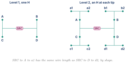
The tree is balanced by geometry, so you trust a shape rather than a measurement. It costs enormous wire, because you deliberately route short paths the long way.
2.2 Clock tree synthesis
Real flops cluster around register files and are sparse under big SRAMs, so a pure H-tree wastes symmetry on empty regions. Clock tree synthesis, always called CTS, builds the real tree by inserting buffers and detours until arrivals land inside a target. Insertion delay is source to average sink, typically 300 to 800 ps, and a deep tree is more sensitive to voltage and temperature. Skew is the spread across sinks, and at 3 GHz a 30 ps target is 9 percent of the period, subtracted from setup one way and added to hold the other. On-chip variation acknowledges that two identical buffers do not have identical delay, so signoff derates launch and capture paths in opposite directions. Useful skew is deliberate abuse of the mechanism, pushing one capture flop's clock 20 ps later to close a failing setup path and borrowing that 20 ps from its hold margin.
Gating interacts with all of it. Gating one flop saves that flop's clock pin, but gating a branch feeding 512 flops saves 512 pins plus the buffers and wire on that branch, which is where most of the energy was. And a gating cell sits on the clock path, so it delays that branch and manufactures skew between gated and ungated regions, landing on hold paths that cross the boundary.
2.3 Switching clock sources, and the runt pulse
Section 1.4 left you needing to swap running clocks. The naive version is one line.
| assign clk_out = sel ? clkB : clkA; // NEVER do this on a clock |
sel comes from control logic asynchronous to both clocks, because being synchronous to one still leaves it asynchronous to the other. So it can change at any instant, including mid-pulse.
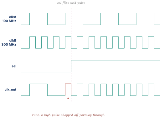
Because sel is asynchronous to both clocks, the truncated pulse can be any width from zero upward. There is no lower bound. You may produce a 40 ps pulse against a flop needing 80 ps of minimum pulse width to complete its internal master-slave handoff, and that flop may capture, may not, or may go metastable. What makes it catastrophic is that the runt is on the clock, so it hits every flop in the domain at once. A data glitch corrupts a value. A clock glitch corrupts the machine.
The correct structure is a glitch-free clock mux, a mutual-exclusion interlock where each source has an enable that may only turn on after the other has been seen off.
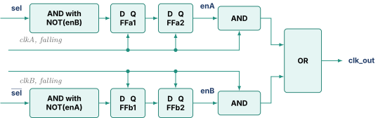
Three details carry it. The enable flops clock on the falling edge, so an enable changes while its clock is low and the final AND never chops a high pulse. Each side's enable is gated by the other's, so both can never be on. And each side uses two flops, which is the synchronizer of Part 5, because sel is asynchronous to both. The cost is dead time, two clkA cycles off plus two clkB cycles on, about 27 ns here with no clock at all, which is why the block must be quiesced first and why frequency changes are orchestrated by an always-on controller.
2.4 Spread spectrum clocking
A perfect 3 GHz clock is the worst case for radio interference, because all its energy sits in a narrow line and regulators measure peak energy in a band. Spread spectrum clocking sweeps the frequency slowly, say between 2.985 and 3.000 GHz on a 33 kHz triangle, smearing the same energy over 15 MHz and dropping the measured peak by 8 to 12 dB. It costs a little setup margin as extra clock uncertainty. More subtly, a spread domain and a non-spread domain now have a continuously drifting phase relationship by construction, so signals between them are genuine asynchronous crossings even when both clocks came from the same PLL at the same nominal frequency.
03.Part 3, metastability
3.1 The assumption that just died
The central picture in Digital Logic and Timing was launch flop, logic, capture flop, both on the same clock. That shared clock fixed the gap between launch and capture at exactly one period, so a tool could add delays and prove arrival. Put the flops on different unrelated clocks and there is no fixed relationship, no "one period later," nothing to add up. The question "does the data arrive in time" has no answer, because the deadline moves.
3.2 Why the violation is guaranteed, not merely likely
The first instinct is that a violation is unlikely and you can probably get away with it. Quantify it and that instinct dies. Take the friendliest case, two clocks nominally at 300 MHz from separate crystals each good to 50 ppm, so worst case 100 ppm apart. The period is 3.333 ns, so relative phase slips by
which sounds like nothing. But it never stops. Sliding through a full period takes cycles, which is 33 µs. Every 33 microseconds the capture edge sweeps through every possible position relative to the data transition, including the setup and hold window. If that window is 50 ps, the fraction of the sweep inside it is percent, which at 300 MHz is 4.5 million dangerous sampling opportunities per second. This is not a rare corner. It is a certainty repeating tens of thousands of times a second, and no constraint and no cell choice changes it.
3.3 The ball on the hill
Inside the flop is a pair of cross-coupled inverters, each output feeding the other's input. It has two stable states and one exactly balanced point where both nodes sit at VDD/2, and that point is an equilibrium that is unstable.
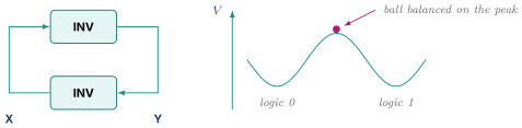
At a clock edge the flop pushes the ball, with a push whose strength is proportional to how far the data input sits from the switching threshold at that instant. Data changing right at the edge gives a tiny push, and the ball can land on the peak. That flop is metastable. Its output is neither a valid 0 nor a valid 1, it may sit at an intermediate voltage or drift or oscillate, and it stays there for an unbounded time until noise tips it.
3.4 Why metastable is worse than wrong
Suppose the flop merely captured the wrong value, grabbing the old 0 when the source had gone to 1. Usually not a disaster. Every consumer sees a consistent 0, the design behaves as though the transition happened a cycle later, and for an asynchronous status bit you had already accepted that.
Metastability is categorically different, and the reason is inconsistency. The node sits at 0.40 V with VDD at 0.80 V. Two gates read that wire, and because of manufacturing variation gate A switches at 0.38 V while gate B switches at 0.42 V. Gate A reads a 1. Gate B, at the same instant on the same wire, reads a 0. That cannot happen with a wrong value, because a wrong value is at least a value.
Concretely, say the node feeds an FSM's next-state logic, which reads 1 and advances to BUSY, and also a valid flag, which reads 0 and stays low. The FSM now waits for a transaction that was never marked valid, and waits forever. The design deadlocks in a state combination the designer proved unreachable. The proof was not wrong. The proof assumed every wire has one value everybody agrees on, and metastability breaks that assumption.
3.5 The waveform
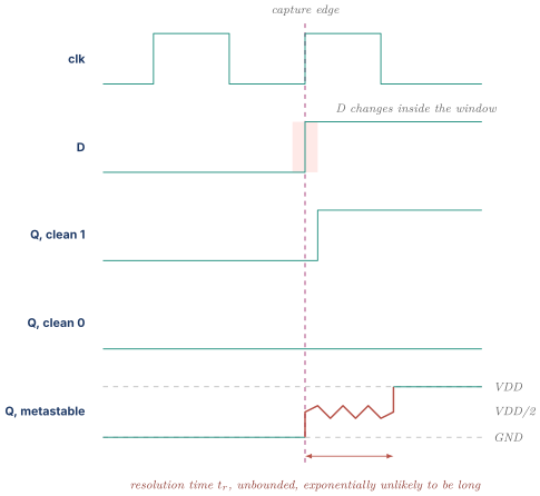
What the picture cannot show is that during the wiggly region, different downstream gates disagree about what they are looking at.
04.Part 4, the exponential that saves us
4.1 Why the ball leaves the peak
The cross-coupled pair is an amplifier with feedback, and such a thing does not sit at an unstable point. A one microvolt imbalance gets amplified, pushing the node further off balance, which gets amplified again. The imbalance grows exponentially with time constant , in a modern process 10 to 30 ps. How long does 1 µV take to become a full 0.8 V swing at ps?
Even from an absurdly small imbalance, resolution takes a few hundred picoseconds. Turn it around and the survival probability is . Exponential decay is extraordinarily fast. Doubling the wait does not halve the probability, it squares it.
4.2 MTBF, term by term
is the metastability window, the aperture around the edge in which a data transition can cause metastability. It is not exactly , it is an empirically fitted characterization parameter, typically tens of picoseconds. is the sampling rate, since more samples means more chances. is how often the asynchronous input changes, since a signal that never toggles carries no risk. Their product is metastable events per second. The numerator is the payoff, where is how long you let the flop sit before anything reads it, and every of extra waiting divides the failure rate by .
4.3 One flop, worked
Fix ps, ps, MHz so ns, and MHz. The denominator is the same for every case below.
The naive design has one flop whose output feeds logic almost immediately, so ns.
Divide by 86400 and that is 5.6 days. Ship a million units and roughly 180,000 enter an undefined state every day, and the failure is a deadlock rather than a graceful error.
4.4 Two flops, worked
Feed the first flop into a second flop on the same clock and let nothing else touch the first flop's output. The metastable node now gets a full period, so ns.
The universe is about seconds old, so this is roughly times the age of the universe. One extra flip-flop moved failure from weekly to never, for one flop and one cycle of latency. That is why the two-flop synchronizer is universal.
4.5 The row that should worry you
Repeat at 2 GHz where ns, holding everything else fixed.
| Configuration | denominator | MTBF | in human terms | |||
|---|---|---|---|---|---|---|
| 1 flop, 500 MHz | 0.5 ns | 25 | s | 5.6 days | ||
| 2 flops, 500 MHz | 1.9 ns | 95 | s | never | ||
| 2 flops, 2 GHz | 0.4 ns | 20 | s | 13 minutes | ||
| 3 flops, 2 GHz | 0.9 ns | 45 | s | 1.8 million years |
Row three is the useful one. The same two-flop synchronizer that was bulletproof at 500 MHz fails every 13 minutes at 2 GHz. That explains a decision people otherwise treat as superstition, since fast domains use three-flop synchronizers or dedicated high-gain synchronizer cells with smaller . The caveat is that a process capable of 2 GHz would have a smaller than one running at 500 MHz, so holding fixed overstates the size of the effect. The direction is real regardless, since shrinking the resolution window shrinks the exponent, and the exponent is everything.
05.Part 5, the synchronizer, and everything it does not fix
5.1 The structure, and the node nobody may touch
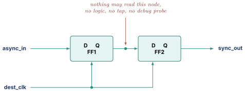
Both flops sit on the destination clock. FF1 does the dangerous sampling and may go metastable, FF2 samples it a full period later, and Part 4 has almost certainly resolved it by then. Place the flops adjacent, because every picosecond of wire between them is stolen from in the exponent, and prefer the library's dedicated synchronizer flops with higher gain and smaller .
The constraint in the diagram is the mechanism, not a style preference. The synchronizer works because FF1's output is metastable and nobody looks at it. Attach logic and you have handed a metastable voltage straight to the fabric, and 3.4 applies in full. This is exactly what static CDC tools check. One assign that ANDs FF1's output with an enable, added to save a cycle, silently converts a correct synchronizer into a broken one.
5.2 The latency, and its uncertainty
A two-flop synchronizer costs one to two destination cycles, and the spread is fundamental. With destination edges at 0, 5, 10, 15, and 20 ns, a source signal rising at 4.9 ns is caught at 5 and presented at 10, while one rising at 5.1 ns misses that edge, is caught at 10, and is presented at 15. A 0.2 ns difference at the source became a 5 ns difference at the destination. So any protocol across a crossing must be latency-insensitive, working whether a response takes two cycles or three. Anything that counts cycles across a crossing is broken by construction.
5.3 The multi-bit failure
A synchronizer makes a bit safe. It does not make a bus safe.
Take a 4-bit value going from , which is 7, to , which is 8. Give every bit its own perfectly correct two-flop synchronizer, so every bit is individually guaranteed to resolve to a valid 0 or 1. The problem is that they resolve independently, each tipping its own way at its own moment.
| Destination cycle | bit3 | bit2 | bit1 | bit0 | reads as | ever valid at source? |
|---|---|---|---|---|---|---|
| 0 | 1 | 1 | 1 | 7 | yes, old value | |
| 1 | 1 | 1 | 1 | 15 | no, never existed | |
| 1 | 0 | 0 | 0 | 8 | yes, new value |
For one cycle the destination read 15, a value never present at the source. A different resolution order gives , equally fictional. If that were a FIFO write pointer, the reader would conclude there were 15 entries and read eight words of garbage. Every bit was captured correctly. The word was not. No number of extra flops fixes it, because each bit still resolves independently. You are no longer fighting metastability, you are fighting coherence, and coherence needs a structural answer.
5.4 Answer one, Gray coding
If the failure comes from several bits changing at once, arrange for only one to change. Then both possible readings correspond to a value that genuinely existed. Gray code has that property, converting with .
| Decimal | Binary | Gray | Bits changed from previous |
|---|---|---|---|
| 2 | 010 | 011 | 1 |
| 3 | 011 | 010 | 1 |
| 4 | 100 | 110 | 1 |
| 5 | 101 | 111 | 1 |
Look at 3 to 4, the transition that broke everything. Binary changes all three bits. Gray changes exactly one. Check by hand, where and . The catch is that this only helps values that step by one, meaning counters. A Gray-coded arbitrary data bus is meaningless, because the previous value has no relationship to the current one. That is why FIFO pointers are Gray coded and FIFO data is not.
5.5 Answer two, the handshake
If the data cannot be made single-bit-changing, hold it still while it is read and synchronize only a flag saying when still is true.
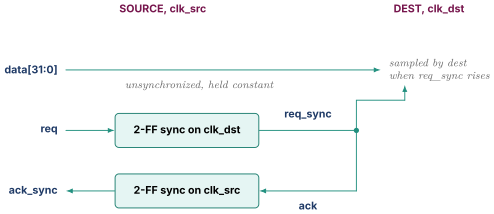
The source drives data, lets it settle, raises req, and two destination cycles later req_sync rises and only then does the destination sample. The source may not touch data until it sees ack_sync, so the bus is stable during the sample and there is no metastability on the data bits at all. The data bus is never synchronized, and that is the point. Cost is two destination cycles out, two source cycles back, plus turnaround, so four to six cycles of the slower clock per word. With a 1 GHz source and a 100 MHz destination that is about 50 ns per 32-bit word. Fine for configuration registers, useless for bulk data.
5.6 Answer three, the asynchronous FIFO
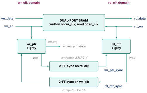
The memory needs no synchronization because the two ports never touch the same location at once, which the pointers guarantee. Only the pointers cross, they are Gray coded so they cross one bit at a time, and each side compares its live pointer against a synchronized copy of the other's.
Now the elegant part. The copy you compare against is stale by two cycles, and that does not break anything because staleness always errs safely. The write side computes full from a stale read pointer that lags the real one, so the FIFO looks more full than it is and you might refuse a write when there was room. The read side computes empty from a stale write pointer, so it looks more empty than it is and you might stall a read when a word had arrived. Both are conservative, and overflow and reading garbage, the only things that must never happen, cannot be caused by staleness.
5.7 Pulse and toggle synchronizers
A two-flop synchronizer works on levels. Hand it a single-cycle pulse from a fast domain into a slow one and it loses it, because at 1 GHz a pulse is 1 ns wide while a 100 MHz destination looks every 10 ns. Convert the event into a level change that persists.
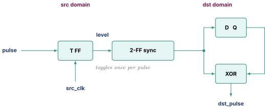
The source toggles a flop on every pulse, so the level flips 0, 1, 0, 1 and each flip records an event. The destination synchronizes the level, then XORs it with a one-cycle-delayed copy of itself, producing a one-cycle destination pulse per toggle. The limitation is a rate limit, since the destination needs two or three of its own cycles per toggle. With a 1 GHz source and a 100 MHz destination, pulses must be at least 30 ns apart, which is 30 source cycles. Send them faster and toggles are lost, and at that point you want the FIFO from 5.6.
5.8 Reconvergence, and choosing
One failure survives even when everything above is correct. Two related control bits, each correctly synchronized through its own two-flop synchronizer, feed the same downstream logic. Each is individually safe, but they can resolve on different cycles, so the logic sees a combination never valid at the source. Take a 2-bit one-hot state where is IDLE and is BUSY. The source goes IDLE to BUSY, so both bits change, and the destination can observe , meaning no state, or , meaning both. A one-hot decoder handed issues two grants and handed issues none. The rule is short. Synchronize one bit and derive the rest.
| What crosses | Structure | Latency | Constraint |
|---|---|---|---|
| One control bit, level | 2-FF synchronizer | 1 to 2 dest cycles | nothing may tap the middle node |
| One bit, very fast clock | 3-FF synchronizer | 2 to 3 dest cycles | when the MTBF math demands it |
| Single-cycle pulse to a slower domain | toggle synchronizer | 2 to 3 dest cycles | pulses 3 dest periods apart |
| A counter or pointer | Gray plus 2-FF | 2 dest cycles | must change by one step |
| Arbitrary multi-bit, low rate | 4-phase handshake | 4 to 6 slow cycles | data held stable, not synchronized |
| Arbitrary multi-bit, high rate | asynchronous FIFO | 2 to 3 dest cycles | dual-port RAM, Gray pointers |
| Reset release | reset synchronizer | 2 dest cycles | Part 7 |
06.Part 6, reset
6.1 What reset is for
At power-up every flip-flop holds an arbitrary value, decided by which side of its cross-coupled pair won the race as the supply rose. Not zero. Arbitrary. A 64-bit program counter powers up at a random address and the core fetches from it. A one-hot state vector powers up with three bits set and its decoder issues three conflicting commands. A FIFO powers up with write pointer 9 and read pointer 3, believing it holds six words that were never written.
Reset forces a known state so the first real cycle starts somewhere the designer reasoned about. Not every flop needs it, since deep datapath pipeline registers have their garbage flushed by the first real transactions. Control flops, state machines, pointers, and valid bits always need it, because a wrong value there is acted upon rather than flushed. In a 200,000-flop core with 40 percent coverage that is 80,000 reset sinks, nearly the routing problem the clock is, except that reset toggles once per power cycle so it costs area and not power.
6.2 Synchronous reset, and how clock gating kills it
Synchronous reset treats reset as ordinary data, sampled by the clock like any other input.
| always_ff @(posedge clk) begin | |
| if (!rst_n) count <= '0; | |
| else count <= count + 1'b1; | |
| end |
It has real advantages. Reset is just a data input, so STA handles it with no special constraints or checks, a glitch shorter than a clock period is filtered out by the sampling, and release is aligned to the clock by construction.
It has one fatal flaw. It needs a running clock. A block goes idle, power management gates its clock off, reset asserts, and nothing happens because there is no edge to sample it. Reset deasserts 100 ns later, still nothing. The clock returns and the block resumes with its old state, having missed the reset entirely. The same problem appears with slow domains, where a 10 ns reset pulse into a 100 kHz domain with a 10 µs period is missed completely. Synchronous reset requires the pulse to be at least one period of the slowest clock that must see it.
6.3 Asynchronous reset, recovery and removal
Asynchronous reset drives a dedicated flop pin that forces the output immediately, with no clock involved.
| always_ff @(posedge clk or negedge rst_n) begin | |
| if (!rst_n) count <= '0; // effective the instant rst_n falls | |
| else count <= count + 1'b1; | |
| end |
That works with the clock stopped, gated, or not yet started, which is why it is the SoC default and why power-up can assert reset before the PLL has locked. Assertion is the easy half. Release is the hard half, because the reset pin has its own timing requirements against the clock edge, and they are the exact analogues of setup and hold. Recovery time is how long reset must already be deasserted before an edge, the setup analogue. Removal time is how long it must remain asserted after an edge, the hold analogue.
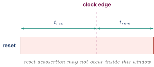
With ns on a 2 ns clock, a reset releasing 0.05 ns before an edge violates recovery by 0.15 ns, and the flop may capture, may not, or may go metastable, now on a control flop that was supposed to hold a guaranteed value. Since reset comes from a pin or a watchdog or a controller on another clock, it is asynchronous by definition, so 3.2 applies and the violation is a certainty rather than a possibility.
6.4 Reset skew
Even with no metastability, a second problem arrives. The reset net is enormous, so like the clock it has skew. Take 300 ps of reset skew against a 3 GHz clock whose period is 333 ps.
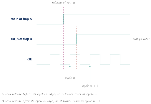
Flop A leaves reset a full cycle before flop B. If they are two bits of the same one-hot vector, the machine spends a cycle in a state that is neither legal nor the reset state. If A is a counter and B its enable, the counter takes a step it should not have. So asynchronous reset gives you assertion that works without a clock, which you need, and release behavior that is unusable as-is.
07.Part 7, the reset synchronizer
7.1 Asynchronous assert, synchronous deassert
Keep the good half and repair the bad half using exactly the two-flop synchronizer of Part 5.
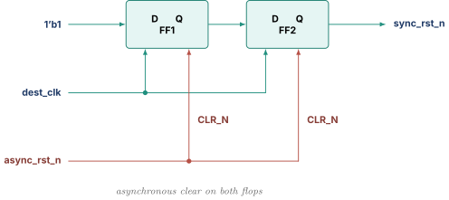
On assertion, async_rst_n falls, both flops clear immediately through their clear pins with no clock required, and sync_rst_n drops instantly. That works with the clock stopped or absent. On release, the clears are removed but both flops still hold 0, and the constant 1 on FF1's D walks through one flop per clock edge, so sync_rst_n rises exactly on a clock edge.
| Event | async_rst_n | FF1.Q | FF2.Q = sync_rst_n | Comment |
|---|---|---|---|---|
| in reset | 0 | 0 | 0 | cleared asynchronously, no clock needed |
| release at | 1 | 0 | 0 | clears removed, D=1 waiting at FF1 |
| first edge | 1 | 1 | 0 | FF1 may go metastable here |
| second edge | 1 | 1 | 1 | FF1 had a full period to resolve, clean release |
FF1 absorbs the danger, since its clear was removed at a moment unrelated to the clock and it can violate its own removal time. FF2 gives it a full period, and the MTBF arithmetic of Part 4 applies unchanged.
7.2 Why D is tied high
The D input's only job is to supply the value meaning "reset is over." With active-low reset that value is 1. It is a constant because there is no data here, only a release event, and the event is communicated by the clear pins going inactive rather than by anything arriving on D. Put differently, the structure is not synchronizing a signal, it is synchronizing the removal of an asynchronous clear, and the constant 1 is what propagates once the clear is gone. With active-high reset you would tie D low and use asynchronous preset.
7.3 One synchronizer per clock domain
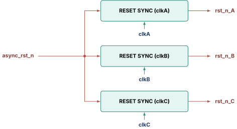
Every domain asserts at the same instant, because assertion is asynchronous and shared. Every domain releases on its own clock two of its own cycles later, so release is coherent within each domain even though domains release at different absolute times. That last clause creates Part 8.
One operational trap. If a domain's clock is not running when async_rst_n releases, its synchronizer never advances and the domain stays in reset. That is correct and safe, but it means clock enable and reset release must be sequenced, and a controller that releases reset and forgets to enable the clock produces a block that is silently dead.
08.Part 8, reset domain crossing
8.1 The failure, and why the tools miss it
Every modern SoC has a dozen or more reset domains so blocks can be reset independently, and that creates the reset analogue of CDC.
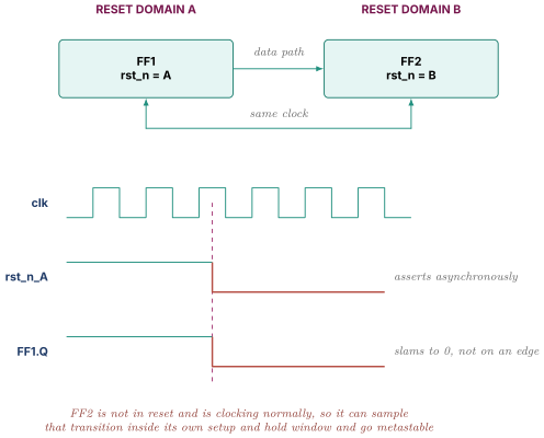
FF2 was never in reset, so nothing forces it back to a known state afterward. If FF2 is part of a state machine in domain B, that machine can sit in an illegal state, in a design where domain B was supposed to be untouched by domain A's reset.
A CDC tool partitions by clock, finds paths whose launch and capture clocks differ, and checks those for synchronizers. Here FF1 and FF2 are on the same clock, so there is no clock domain crossing, and the tool sees an ordinary intra-domain path and reports nothing. STA misses it for a more interesting reason, since STA analyzes a data path assuming the launch flop changes only at a clock edge, and that assumption is what lets it add to the launch edge and compare against capture. An asynchronous reset makes the launch flop change at a moment that is not an edge, and STA has no timing arc for that. It is not that STA gets the answer wrong. The event is outside its model of what can happen.
So the path is invisible to both tools you would expect to catch it. And RDC bugs only manifest when one domain resets while another stays live, which is exactly what partial power-down and per-core reset do, and exactly what a bring-up test that resets everything at once never exercises.
8.2 What to do about it
Put both flops in the same reset domain, so there is no crossing. This is an architecture-time partitioning decision and by far the cheapest fix, which is why reset boundaries should follow functional boundaries. Synchronize the crossing signal in the destination reset domain, absorbing the metastability as in Part 5, at the cost of latency. Qualify the data with a signal held low during the reset event, so the destination never samples a transitioning value. Isolate at the boundary with a clamp cell holding the signal at a safe constant while the source is in reset or powered down, which is the same mechanism power domain isolation uses in Power Fundamentals and Clock Gating.
Scale matters. Twelve reset domains give ordered domain pairs, and a real RDC run on a large SoC reports thousands of crossings needing triage. Most get waived as functionally impossible, and the waiver file becomes a maintained design artifact.
8.3 Reset sequencing
Release order matters as much as mechanism, and getting it wrong produces hangs rather than corrupt data. A representative bring-up order is power good, then reference clock stable, then PLL enabled and locked, which is the 20 to 100 µs of 1.4, then dividers programmed and clock enabled, then the always-on domain's reset released, then the interconnect, then cache and memory, then the core last. Two rules govern it. Clocks before resets, because a reset synchronizer with no clock never releases, per 7.3. And producers before consumers, because a consumer released early issues requests into a block still in reset.
Concretely, release the core before the interconnect and the core immediately fetches. The interconnect is in reset and drops the request without responding. The load-store unit waits forever for a response that will never come, and the machine hangs on its first instruction with no error indication anywhere. Debug on that is miserable, because the symptom is total silence. Sequencing is driven by a small always-on state machine watching PLL lock and power-good, which is precisely what a Resource Controller contains.
09.Part 9, verification
A testbench writes always #5 clkA = ~clkA; and always #1.667 clkB = ~clkB;, and those clocks are exactly rationally related in the event queue, so the phase relationship repeats and never sweeps. The simulator has no concept of a partial edge, no setup check on an unconstrained path, and no model of metastability. So a crossing with no synchronizer at all simulates perfectly in every regression, then fails intermittently in the lab in a way that depends on temperature. That is why CDC is checked structurally rather than dynamically.
A CDC tool does two passes. The structural pass computes which clock drives each flop, finds paths where launch and capture clocks differ, and checks for a recognized synchronizer, flagging unsynchronized crossings, logic between synchronizer stages, fanout from the first stage, multi-bit crossings without Gray coding or a handshake, and reconvergence. The protocol pass is formal, proving things like "source data is stable for destination cycles around each req." A structurally correct handshake with a broken protocol still fails, so the second pass is not optional. The commonest reason a CDC run is worthless is a bad setup, since declaring two genuinely asynchronous clocks as one clock group makes every crossing between them invisible. RDC analysis is the same shape with reset domains substituted, and most of the engineering is building a defensible waiver set.
A useful complement is making simulation pessimistic on purpose, replacing synchronizer outputs with models that randomly delay the transition by a cycle or drive X, so the design is exercised against the one-cycle uncertainty of 5.2 rather than the simulator's determinism. This is where the material connects to Verification Methodology.
10.Part 11, check yourself
- Why can you not build a chip's timebase from a ring oscillator, and why can you not buy a 3 GHz crystal? (1.1)
- Walk through a PLL block by block, saying what problem each solves, then state the relationship between the feedback divider and output frequency. (1.2, 1.3)
- A PLL takes 50 µs to relock. Convert to cycles at 3 GHz and explain what that forces DVFS to do instead. (1.4)
- Contrast a PLL and a DLL. Why does jitter accumulate in one and not the other? (1.6)
- Estimate clock network power for a 200,000-flop core, then explain why gating high in the tree saves more than gating at the leaves. (2.1, 2.2)
- Why can a plain mux not switch between two running clocks? What does a runt pulse do, and why is it worse than a data glitch? (2.3)
- Two clocks are nominally equal from crystals 100 ppm apart. Show with arithmetic that a violation is guaranteed rather than merely likely. (3.2)
- Explain metastability to someone who believes the flop just captures the wrong value. Why is inconsistency the real problem? (3.3, 3.4)
- Write the MTBF formula and work the one-flop and two-flop cases at 500 MHz, then explain why the same synchronizer is inadequate at 2 GHz. (4.2, 4.3, 4.4, 4.5)
- Why must nothing read the intermediate node of a two-flop synchronizer? (5.1)
- You synchronize a 4-bit value going 0111 to 1000 through four correct synchronizers. Show what goes wrong, explain why more flops do not help, and give three structural fixes. (5.3, 5.4, 5.5, 5.6)
- Why are async FIFO pointers Gray coded, and why is it safe that each side compares against a stale copy of the other pointer? (5.4, 5.6)
- A single-cycle pulse in a 1 GHz domain must reach a 100 MHz domain. What breaks, what do you build, and what rate limit does it impose? (5.7)
- Compare synchronous and asynchronous reset. Why does clock gating break the synchronous kind, and what are recovery and removal? (6.2, 6.3)
- Draw a reset synchronizer. Why are the D inputs tied high, and why are two flops needed? (7.1, 7.2)
- What is reset domain crossing, and why do CDC and STA both miss it? (8.1)
- Give the reset release order for a core coming out of power-up, and say exactly what hangs if you release the core before the interconnect. (8.3)
11.Part 12, related notes
- Digital Logic and Timing for setup, hold, skew, and jitter, which every equation here is built on
- Power Fundamentals and Clock Gating for why the clock tree is gated and for isolation cells at domain boundaries
- DVFS Droop and Thermal for why frequency switching happens and why relock latency shapes the mechanism
- RTL Design and SystemVerilog for the coding patterns that implement synchronizers and reset correctly
- Verification Methodology for where CDC, RDC, and formal property checking sit in signoff
- STA Synthesis and Physical Design for CTS, on-chip variation, and useful skew as physical-design activities
- Arbiters FIFOs and CAMs for the synchronous FIFO the async FIFO is built on
- Sequential Logic and Timing for the vault's shorter treatment of metastability and CDC