DVFS, Voltage Droop, Adaptive Clocking, and Thermal Management
September 8, 202676 min readadvanced
Start from the delay model in Digital Logic and Timing. A gate's delay is the time it takes to move charge onto or off a capacitance,
01.Part 1, why voltage is the master lever
1.1 The quadratic answer, and why it is only half the answer
From Power Fundamentals and Clock Gating, dynamic power is
Voltage appears squared, which already makes it the strongest term. Ask most candidates what happens when you cut the supply by 20 percent and they answer that power falls by 36 percent, because . That answer is arithmetically correct and physically incomplete, and the gap between the two is the most important idea in this note.
The reason is that and are not independent. You cannot simply turn the voltage down and leave the clock where it was. Lowering the supply makes every gate slower, and if the gates get slower while the clock stays fast, the critical path no longer fits inside a clock period and the chip fails setup timing. So a voltage reduction forces a frequency reduction, and the frequency reduction contributes its own linear saving on top of the quadratic one.
1.2 Deriving the frequency-voltage relationship rather than asserting it
Start from the delay model in Digital Logic and Timing. A gate's delay is the time it takes to move charge onto or off a capacitance,
The voltage swing is the supply itself, so the numerator grows in direct proportion to . The denominator is the drive current the transistor can supply, and that depends on the overdrive, meaning how far the gate voltage exceeds the threshold, . For a textbook long-channel device the saturation current goes as . Real short-channel devices hit velocity saturation, where the carriers stop speeding up no matter how hard you push, and the exponent collapses toward 1. Measured devices in modern processes sit around
That is the velocity saturation index and it is a fitted number, not a derived one. Put the two together and the maximum clock frequency, which is the reciprocal of the critical path delay, goes as
That does not look linear in . Work it with numbers and it very nearly is. Take V and , and normalise everything to the 1.0 V point.
| relative | relative | verdict | ||||
|---|---|---|---|---|---|---|
| 1.00 | 0.70 | 0.629 | 0.629 | 1.000 | 1.00 | reference |
| 0.90 | 0.60 | 0.515 | 0.572 | 0.909 | 0.90 | linear to within 1 percent |
| 0.80 | 0.50 | 0.406 | 0.508 | 0.807 | 0.80 | linear |
| 0.70 | 0.40 | 0.304 | 0.434 | 0.690 | 0.70 | linear |
| 0.60 | 0.30 | 0.209 | 0.348 | 0.553 | 0.60 | starting to fall faster |
| 0.50 | 0.20 | 0.123 | 0.247 | 0.392 | 0.50 | clearly sublinear |
| 0.40 | 0.10 | 0.050 | 0.125 | 0.199 | 0.40 | collapsing |
Look at the two rightmost numeric columns between 1.0 V and 0.7 V. They track each other to within a percent or two. Over that range, and that is the range a product actually operates in, frequency scales linearly with voltage, and it does so not because anyone designed it that way but because the growth of happens to almost exactly cancel the in front of it. Below about 0.6 V the cancellation breaks down, because is shrinking much faster in relative terms than is, and frequency falls off a cliff. That cliff is the subject of 1.5.
1.3 The cube law, worked
Now substitute. If then
Power scales with the cube of voltage. Put real numbers on a 20 percent supply reduction so the result is yours rather than something you memorised.
Start at 1.00 V and 3.0 GHz, and say the core burns 5.0 W there. Drop to 0.80 V. From the table, falls to 0.807 of its old value, so round it to 2.4 GHz, which is exactly 0.8 of 3.0 GHz. Then
The core now burns W. A 20 percent voltage reduction cut power essentially in half. The quadratic answer would have predicted 3.2 W. The extra 0.64 W of saving came entirely from the frequency term that the quadratic answer forgot about.
Run it in the other direction, because the other direction is where the pain lives. To go from 2.4 GHz to 3.0 GHz, a 25 percent frequency increase, you must raise voltage by 25 percent and power goes up by . The last 25 percent of frequency costs you 95 percent more power. That single sentence explains why the fastest bin of any product line is disproportionately hot, why turbo is time-limited, and why efficiency cores exist at all.
A useful small-signal shortcut falls out of the cube law. Differentiating gives , so every 1 percent of voltage costs about 3 percent of power. That approximation is good to within a few percent out to about a 10 percent voltage change, and it is the fastest way to price a guardband decision in your head during an interview.
1.4 Energy per operation, and why battery life is a different question
Power is watts. Battery life is joules. They are not the same question and conflating them is a classic error.
Take a fixed job of 1 billion cycles. At 1.00 V and 3.0 GHz it takes s at 5.0 W, so it consumes J. At 0.80 V and 2.4 GHz the same billion cycles take s at 2.56 W, consuming J.
The job took longer and used less total energy, 1.07 J instead of 1.67 J, a 36 percent saving. Check that against the algebra. Energy for fixed work is . And indeed . Energy per operation scales with the square of voltage.
That is the fact that matters for a phone. A battery holds a fixed number of joules. Cutting voltage 20 percent buys 36 percent more work out of the same charge, entirely independent of how long you are willing to wait. Cutting frequency alone, holding voltage fixed, buys nothing in energy, because power falls linearly and time rises linearly and the product is unchanged. That is the point Power Fundamentals and Clock Gating makes in its lever table and it is worth repeating here. Frequency is only an energy lever when it drags voltage down with it.
Put the energy scale in perspective with public per-operation figures, which are usually quoted from Horowitz's ISSCC 2014 survey at 45 nm. They are old and the absolute numbers have shrunk since, but the ratios have barely moved and the ratios are the lesson.
| Operation | Energy, 45 nm | Relative to an integer add |
|---|---|---|
| 32-bit integer add | 0.1 pJ | 1 |
| 32-bit floating point add | 0.9 pJ | 9 |
| 32-bit integer multiply | 3.1 pJ | 31 |
| 32-bit read from an 8 KB SRAM | 5 pJ | 50 |
| 32-bit read from off-chip DRAM | 640 pJ | 6400 |
Two conclusions follow, both architectural rather than circuit-level. Moving data costs vastly more than computing on it, which is why cache hierarchies exist for power reasons and not only for performance reasons, and it connects to Cache Organization and Prefetching. And in an out-of-order machine the arithmetic is a small fraction of the energy of executing an instruction, because fetch, decode, rename, allocate, schedule, wake up, and retire all burn energy before the ALU does anything, which is why Out of Order Execution is a power topic as much as a performance topic and why widening a machine is not free.
Performance per watt is operations per second divided by joules per second, which cancels to operations per joule, the reciprocal of energy per operation. Perf-per-watt and energy-per-operation are the same statement in different units. The related energy-delay product exists because pure energy minimisation would drive you to run everything infinitely slowly, and under the model above , so even EDP keeps falling as voltage drops and you need before the optimum lands somewhere sensible. These metrics disagree about the optimum, and the choice among them is a product decision rather than a physics one.
1.5 Where the cube law stops being true
Three separate floors stop you from riding the cube law to zero, and naming all three is what distinguishes understanding the model from reciting it.
The frequency collapse. From the table in 1.2, below roughly the overdrive shrinks so fast in relative terms that frequency falls faster than voltage. Once that happens, energy per operation stops improving, because time stretches faster than power drops.
The leakage floor. Leakage is paid per unit time, not per operation, and from Power Fundamentals and Clock Gating it does not care whether anything switches. So as you slow down, leakage energy per operation rises in proportion to how long the operation takes. There is a genuine minimum-energy point where falling dynamic energy and rising leakage energy cross, typically just above threshold and very slow. Near-threshold computing lives there and accepts a factor of ten in frequency for roughly a factor of five in energy, which is a real research area and a poor fit for a CPU that has to feel responsive.
The array Vmin floor. This is the one that actually binds. An SRAM bit cell is a pair of cross-coupled inverters that must simultaneously hold state against noise and be readable and writable through access transistors, and those requirements pull the sizing in opposite directions. As the supply falls, the hold, read, and write margins all shrink while random dopant fluctuation makes individual cells diverge from each other, so below some voltage a few cells in a multi-megabit array simply fail, and with millions of cells the one-in-a-million cell is guaranteed to exist. That floor, covered further in SRAM Arrays and ECC, usually sits 100 to 200 mV above the logic's own floor. The fixes are to put the arrays on a separate, higher rail, to use assist circuits that momentarily boost the wordline or collapse the cell supply during a write, or to accept the array floor as the whole domain's floor. Knowing that memory rather than logic sets the bottom operating point is a strong and non-obvious answer.
02.Part 2, DVFS, DVFM, and the sequencing that makes it work
2.1 The operating point table
Dynamic voltage and frequency scaling means adjusting both at runtime to match demand. Some vendors say DVFM, dynamic voltage and frequency management, which describes the same physics framed as a managed system with policy rather than as a bare mechanism. If an interviewer says DVFM, they mean DVFS plus the controller, the policy, the telemetry, and the state machine that arbitrates between competing requests.
You do not scale continuously. You scale between a small set of characterized operating points, each a legal pair of voltage and frequency, sometimes called P-states. Each point was validated in silicon across process corners, across temperature, and with margin for everything in Part 3. A plausible table for a performance core looks like this.
| Point | Relative | Core power at 5 W nominal | Use | ||
|---|---|---|---|---|---|
| P0, turbo | 1.05 V | 3.2 GHz | 1.18 | 5.9 W | short bursts only, thermally limited |
| P1, nominal | 1.00 V | 3.0 GHz | 1.00 | 5.0 W | sustained peak |
| P2 | 0.90 V | 2.7 GHz | 0.73 | 3.6 W | heavy but not peak |
| P3 | 0.80 V | 2.4 GHz | 0.51 | 2.6 W | typical interactive load |
| P4 | 0.70 V | 2.1 GHz | 0.36 | 1.8 W | background work |
| P5, floor | 0.65 V | 1.6 GHz | 0.29 | 1.4 W | array Vmin sets this, not the logic |
Check one row so the table is yours. P3 relative power is , and W. Notice how much of the table's total range sits between P1 and P3, because that is where the cube law bites hardest. Notice also that P5 breaks the linear pattern, dropping frequency a lot for a small voltage drop, because at the bottom you hit the array Vmin floor from 1.5 and cannot go lower on voltage at all, so further power reduction has to come from frequency alone with all its inefficiency.
2.2 The asymmetric sequence, and this is a strong interview answer
This is where the engineering is, and it is asymmetric in a way that most people get wrong on the first try.
Going faster, you raise voltage first. Command the regulator to the new higher voltage. Wait until the voltage has actually arrived at the load, which is not the same as the regulator having been told about it. Only then raise the frequency.
Going slower, you lower frequency first. Drop the clock to the new lower frequency. Confirm it has taken effect. Only then command the regulator down.
The unifying rule underneath both cases is one sentence. At every instant during the transition, the supply must be high enough to support the frequency that is currently running. Draw the two orders as a path through the voltage-frequency plane and it becomes obvious.
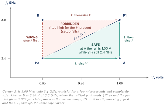
Both correct orders route through corner A, the high voltage, low frequency corner, which is safe and merely inefficient. Both incorrect orders route through corner B, the low voltage, high frequency corner, which is a timing violation.
Now the same thing as a timeline, because in the room you will be asked to draw the handshake rather than the plane.
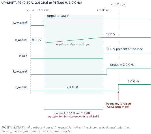
The acknowledge is the part people forget. Commanding the regulator is not the same as the voltage having arrived, and the gap between the two is tens of microseconds. Something must measure or wait for the rail before the frequency is allowed to move, whether that is a regulator status bit, an on-die voltage comparator, or a conservative fixed timer sized against the worst-case slew. A controller that raises frequency on the command rather than on the acknowledge works perfectly in simulation, where the regulator model is instantaneous, and fails in silicon.
2.3 What actually breaks, and why it is worse than a crash
Say it precisely rather than saying "it breaks". At corner B the supply is 0.80 V while the clock is running at 3.0 GHz. The critical path was characterized to take 417 ps at 0.80 V, from the frequency table in 1.2. The clock period at 3.0 GHz is 333 ps. The path needs 84 ps more than it is given, so at the capture flop the data arrives after the setup window has closed.
What happens next is the part worth articulating. A setup violation does not produce an error signal. There is no exception, no machine check, no assertion. The flop captures whatever voltage was on its D pin at the sampling instant, which might be the old value, might be the new value, or might be a partially-settled level that resolves to either one, or that leaves the flop metastable for an unbounded time in the sense of Clocking Reset and Domain Crossing. The wrong bit then propagates into architectural state and corrupts a result silently.
Three properties make it a nightmare in the lab. It is data dependent, because only the operands that actually exercise the critical path see the failure, so most instructions are fine. It is temperature and voltage dependent, so it comes and goes as the part warms up. And it is die dependent, so a fast die in the corner of the wafer never shows it and a slow die shows it constantly. That combination produces the worst bug class in silicon, an intermittent corruption that only reproduces on some units under some workloads at some temperatures, and that no software log will attribute to the DVFS controller.
This is also exactly the class of property that formal verification is good at and simulation is bad at. "The frequency select register can never take a value whose required voltage exceeds the currently acknowledged supply level" is a one-line assertion over a state machine, and proving it holds under all input orderings is a proof, not a test. If you wrote formal properties for SoC power management logic, this is the shape of property to describe.
2.4 The latency budget, which is why droop is a completely different problem
Put the timescales next to each other. This table is the reason Parts 4 and 5 exist as separate material rather than as a footnote to DVFS.
| Event | Time | In 3 GHz cycles |
|---|---|---|
| one CPU clock cycle | 0.333 ns | 1 |
| a voltage droop event, first droop | 1 to 5 ns | 3 to 15 |
| ring oscillator droop detection | 2 to 10 ns | 6 to 30 |
| adaptive clock stretch engages | a few ns | ~10 |
| second droop, package resonance | 30 to 100 ns | 100 to 300 |
| glitch-free switch to a divided clock | ~10 ns | ~30 |
| voltage regulator commanded step, settled at the load | 5 to 50 us | 15,000 to 150,000 |
| PLL relock after a frequency change | 10 to 100 us | 30,000 to 300,000 |
| OS or firmware governor decision interval | 1 to 10 ms | 3,000,000 to 30,000,000 |
| thermal time constant of a die hot spot | 1 to 10 ms | millions |
| thermal time constant of a phone chassis | 10 to 100 s | billions |
Read the middle of that table and the whole architecture of power management falls out. A regulator step takes tens of thousands of cycles. A droop is over in ten. No control loop that involves the voltage regulator can possibly respond to a droop. By the time the regulator has heard about the problem, the droop has happened, done its damage, and recovered a thousand times over. Droop must therefore be handled entirely on-die, by circuits that respond in single-digit nanoseconds, with the regulator playing no part at all. That is the reason droop mitigation is its own discipline and not a subsection of DVFS.
The table is also a design principle rather than a list of facts. Every control loop in a power management system must be faster than the phenomenon it controls and slower than the loop beneath it, and the decade-wide gaps between rows are deliberate, because two loops with overlapping bandwidth fight each other and make the operating point hunt. That is why minimum residency times and threshold hysteresis appear at every level of the stack.
2.5 Changing frequency without relocking the PLL
If a PLL relock is tens of microseconds, and it is, per Clocking Reset and Domain Crossing, then any frequency change that has to happen quickly cannot involve relocking. Three standard escapes, in increasing order of cost.
Integer dividers off a running PLL. Leave the PLL locked at some high reference and derive the core clock through a programmable divider. Changing the divide ratio takes a handful of cycles and needs a glitch-free mux so no runt pulse ever reaches the flops. The limitation is that the available frequencies are for integer , so the steps are coarse at the top. From a 3.0 GHz PLL you get 3.0, 1.5, 1.0, 0.75 GHz, and nothing usable between 3.0 and 1.5. Fractional dividers and clock-cycle skipping fill in the gaps at the cost of period jitter that the timing signoff has to absorb.
A second PLL. Keep two PLLs, run on one while the other relocks to the new target, then perform a glitch-free switch. The relock latency is hidden entirely, at the cost of a second PLL's area, power, and its own contribution to supply noise. This is why a cluster often has more PLLs than it has clock domains.
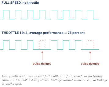
Clock throttling by pulse removal. Rather than changing the frequency at all, delete clock pulses at a controlled duty ratio. Delete one pulse in four and average performance falls 25 percent with a response time of exactly one cycle. Every pulse that is delivered is still full width and full frequency, so nothing violates timing. This is the crudest and fastest lever in the box, it is what an emergency thermal or droop response actually uses, and it costs nothing in silicon beyond a gater from Power Fundamentals and Clock Gating and a small counter. The drawback is that it does not let you lower voltage, so it saves dynamic power in proportion to the throttle ratio and saves no leakage at all. It is a stopgap, not an operating point.
2.6 Per-domain scaling, and the price of it
A heterogeneous SoC does not have one operating point. The performance cluster, the efficiency cluster, the GPU, the neural engine, the fabric, and the memory controller each want their own, because their workloads are unrelated and forcing them to share a rail means every domain pays for the most demanding one.
The benefit is easy to quantify. Suppose the efficiency cluster only ever needs 0.70 V and the performance cluster needs 1.00 V. Share a rail and the efficiency cluster runs at 1.00 V, burning times the power it needed. Split the rails and it burns what it needs. Separate rails for domains with different demand is close to a factor of three on the quiet domain.
The costs land in three places, which is why this is an integration problem rather than a free win. Every signal crossing between independently scaled domains needs a level shifter, because a 0.70 V logic one entering a 1.00 V gate leaves both its transistors partly on and burns steady-state crowbar current, worked out in section 7.2 of Power Fundamentals and Clock Gating. Every clock crossing between them is asynchronous in practice even when both clocks come from the same PLL, because their frequencies change independently and no fixed phase relationship survives, so each crossing needs a synchronizer or an async FIFO per Clocking Reset and Domain Crossing. And each domain needs its own regulator output, which costs pins, package routing, board area, and quiescent power in the regulator itself.
The practical compromise is a hierarchy. A small number of switched, independently scaled rails from the main regulator, then cheap on-die low-dropout regulators fanning out from those to make finer per-block rails wherever the current is small enough that a linear regulator's efficiency loss is tolerable. Section 3.5 explains why that split is the right one.
2.7 Who decides, and how the loop is closed
The controller reads utilization counters, thermal sensors, the power budget, and any explicit hints, then picks a point. A software governor in the OS measures busy fraction over a few milliseconds and writes a P-state request, which is flexible and far too slow to catch a burst lasting 50 microseconds, so it underestimates demand at the start of an interaction and overestimates it after. A hardware autonomous controller runs the loop in firmware or fixed logic with a decision interval of tens of microseconds, reads its own counters, and knows things software cannot, such as measured current and per-sensor temperature. Every modern design is a hybrid, with software supplying quality-of-service and deadline hints and hardware running the fast loop inside them.
Whichever it is, the controller is an arbiter rather than a calculator. It merges requests from multiple agents, respects a global power budget every domain draws from, honours thermal limits that override everything, holds minimum residency so it does not thrash, and sequences the transition per 2.2 without ever entering corner B. That arbitration and sequencing is the interesting logic, and it is exactly what a Resource Controller does.
03.Part 3, guardband, adaptive voltage scaling, and the regulator
3.1 What the margin is actually made of
The operating point table in 2.1 says P1 is 1.00 V. Where did 1.00 come from? Not from measurement of the chip in front of you. It came from taking the voltage at which a typical die closes timing at 3.0 GHz under typical conditions, and then adding margin for every way reality could be worse than typical. That stack of additions is the guardband, and enumerating its components is the first step to attacking it.
| Margin component | What it covers | Typical size on a 1.0 V rail | What can remove it |
|---|---|---|---|
| Global process spread | this die might be a slow one | 50 to 100 mV | per-die AVS with an on-die speed monitor |
| Temperature | characterized at 25 C, running at 95 C | 20 to 50 mV | a temperature sensor in the AVS loop |
| Voltage droop | worst-case transient dip | 50 to 100 mV | decap, adaptive clocking, di/dt control |
| Aging | NBTI and hot carrier degradation over years | 10 to 30 mV | in-situ monitors, periodic re-characterization |
| Model and library pessimism, OCV derates | signoff conservatism from STA Synthesis and Physical Design | 20 to 50 mV | better signoff, statistical timing |
| IR drop across the grid | the far corner of the block is lower than the pin | 20 to 40 mV | better grid, more bumps, local sensing |
Add the midpoints and you get roughly 200 to 250 mV of margin on a rail that might only need 750 mV to actually work. The guardbanded chip runs at 1.00 V when the silicon in front of you, right now, at this temperature, would have worked at 0.78 V.
3.2 Pricing the guardband, which is the argument that makes everything else worth doing
Use the cube law. Running at 1.00 V instead of 0.78 V costs
The fully guardbanded part burns more than twice the power of the same silicon operating at the voltage it genuinely needs. That is not a rounding error and it is not a research curiosity. It is the largest single pool of recoverable power in a modern SoC, larger than anything clock gating can reach, and every technique in the rest of this note exists to claw back some slice of it.
Price a smaller, more realistic slice too. Removing just the droop margin, say 100 mV off a 1.00 V rail, gives , a 27 percent power reduction on every cycle the chip ever runs. Compare that with the clock gating result in Power Fundamentals and Clock Gating, where going from zero to 95 percent coverage bought a 22 percent cut in block dynamic power. One hundred millivolts of droop margin is worth more than an entire aggressive clock gating campaign. That comparison is the single most persuasive thing you can say about why droop mitigation is a discipline.
And note the asymmetry that makes guardband so galling. The margin is sized for the worst case and paid on every cycle. The droop that the 100 mV protects against might occur for 20 cycles out of every million. You pay a 27 percent tax continuously to survive an event with a duty cycle of 0.002 percent. Any mechanism that can detect and respond to the event in real time instead of pre-paying for it wins enormously, and that is the entire logic of adaptive clocking in 5.3.
3.3 Adaptive voltage scaling
Adaptive voltage scaling closes the loop around the guardband. Rather than trusting a fixed table computed at design time for the worst die, measure how fast this die is running right now, and lower the voltage until the measured margin hits a set floor.
The measurement instrument comes in three flavors with genuinely different properties.
A ring oscillator canary is a free-running ring of inverters whose frequency proxies gate speed. Count its edges over a fixed window against a stable reference and you get a number that rises with voltage and falls with temperature. Cheap, tiny, easy to scatter across the die. Its weakness is that a ring of inverters is not the critical path, having no wire load, no complex cells, and no long routes, so it responds to process and voltage in a subtly different ratio than a real path. Good relative measure, poor absolute one.
A critical path replica is a physical copy of the real critical path, or a synthesized structure with the same mix of cell types and wire loads, launched once per cycle. If the signal arrives before the deadline there is margin. It tracks better than a canary because it looks like what it is modelling, but it is still a replica, so it does not sit where the real path sits, does not see the same local IR drop or temperature, and does not age the same way as a path that is actually toggling.
In-situ delay monitors replicate nothing and watch the real paths. A shadow flop beside a real endpoint samples the same data a short delay later, and any disagreement means the data arrived inside that late window, so margin has nearly run out. This is the Razor family, the only method that measures actual paths under actual conditions. The cost is instrumenting enough endpoints to cover the true critical set, which after optimization is often hundreds of near-equal paths rather than one, plus a recovery mechanism for when the warning becomes an error.
Whatever the sensor, the loop is identical. Read the margin indicator, compare against target, adjust the regulator setpoint in small steps with hysteresis so it does not oscillate. Loop bandwidth is set by the regulator, so this runs on microseconds to milliseconds, which is fine because process and temperature move slowly. AVS handles the slow components of the guardband. It cannot and does not handle droop. The two get conflated constantly. The honest caveat to volunteer is that a replica tells you about the replica rather than about the design, so every AVS scheme keeps a residual margin for the mismatch, and shrinking that residual is where the effort goes and why designers deploy many monitors rather than one.
3.4 Adaptive body bias
A fourth transistor terminal exists that nobody teaches first. Besides gate, source, and drain there is the body, also called the bulk or the well, which is the silicon the channel forms in. Bias the body relative to the source and the threshold voltage moves, because you are changing how much charge the gate has to work against to form a channel. Reverse body bias pushes up, making the device slower and much less leaky. Forward body bias pulls down, making it faster and much leakier.
Quantify it from 1.4 of Power Fundamentals and Clock Gating, where the subthreshold slope is about 78 mV per decade. A 100 mV threshold shift is decades, a factor of . A hundred millivolts of body bias is roughly a factor of twenty in leakage. In planar bulk CMOS you got 50 to 100 mV of threshold shift per volt of body bias, which made this a real post-silicon knob. A fast, leaky die gets reverse bias to bring leakage down to spec, a slow die gets forward bias to bring speed up, the process distribution narrows, and yield improves.
Now the honest part, which is what makes this worth mentioning at all. Adaptive body bias largely died with FinFETs. In a fin device the gate wraps the channel on three sides and in a gate-all-around device it surrounds it completely, so the body has almost no electrostatic control left, the body effect coefficient collapses, and the technique stops paying for the well isolation, bias generators, and routing it costs. It survives in FD-SOI, where a thin buried oxide lets a back-gate under the channel exert strong control and bias ranges of a volt or more are useful. Saying that ABB is powerful where the body still has authority and mostly historical in fin-based logic, rather than reciting it as current mainstream practice, signals that you know which process you are talking about.
3.5 Voltage regulators, and why the topology matters to a microarchitect
You do not need to design a regulator, but you need to know what the three kinds cost, because the choice determines your response time, your per-domain granularity, and where the conversion heat lands.
Low-dropout linear regulator, an LDO. A pass transistor in series with the load, controlled by a feedback amplifier that holds the output at target. Conceptually a smart resistor. Every electron delivered to the load passes through the pass device and drops the input-to-output difference across it, so the efficiency is simply
Work it. Converting 1.8 V to 0.9 V at 5 A delivers W and draws W, so 4.5 W is burned in the pass transistor as heat. Fifty percent. Now 1.0 V from a 1.1 V input at 5 A, where the load gets 5.0 W, the input supplies 5.5 W, and only 0.5 W is lost, 91 percent. An LDO is efficient exactly when the conversion ratio is close to one. It is small, needs no inductor, responds in tens of nanoseconds, and is quiet, which makes it perfect for many small local rails derived from a nearby switching rail and terrible for the main conversion from a battery.
Switching buck converter. Chop the input at a few megahertz and filter it with an inductor and capacitor so the average comes out at target. Because it stores energy in the inductor rather than dissipating the difference, efficiency is 85 to 95 percent almost independent of conversion ratio, which is why the main rails come from bucks. The cost is the inductor, a magnetic component that does not shrink well and often cannot go on-die, plus a control loop whose bandwidth is a fraction of the switching frequency. A 2 MHz buck has a loop bandwidth of a few hundred kilohertz and a response time of microseconds. That control loop bandwidth is the third droop tier in 4.5, and it is not a coincidence, it is literally the same loop.
Integrated voltage regulator, sometimes called FIVR. Move the switching converter onto the die or into the package with air-core or thin-film magnetic inductors small enough to integrate. Per-domain rails become cheap, because you stop paying package pins and board area per rail, so a dozen becomes affordable where four was not. Response time drops an order of magnitude because the loop is physically short. And the input rail can be higher, say 1.8 V instead of 1.0 V, which cuts the package current by the same factor and therefore cuts both the drop and the on the way in. The costs are die area, integrated inductors of lower quality so peak efficiency is a few points worse, and conversion loss that now lands as on-die heat in a place you were already trying to cool.
| Property | LDO | Off-package buck | Integrated regulator |
|---|---|---|---|
| Efficiency | , poor for large steps | 85 to 95 percent | 80 to 90 percent |
| Response time | tens of ns | microseconds | hundreds of ns |
| Area or board cost | tiny, on-die | inductor plus caps on board | die area |
| Rails you can afford | many | few | many |
| Where the loss goes | on-die heat | board heat | on-die heat |
| Good for | small local steps | main conversion | per-domain fine control |
04.Part 4, voltage droop, the physics
4.1 The supply is not a voltage source
Everything up to here assumed the chip sees whatever voltage the regulator was told to produce. It does not. Between the regulator's output and a transistor's source terminal there is a long physical path made of board copper, vias, package substrate traces, solder balls, on-package planes, microbumps, and the on-die metal grid, and every centimetre of it has resistance and inductance. Capacitors are deliberately placed at several points along that path. The whole structure is the power delivery network, the PDN, and it behaves like a chain of low-pass filters rather than like a wire.
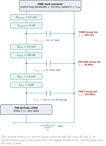
Two structural observations before any arithmetic. First, the capacitors are the only local sources of charge. When the logic suddenly needs more current than the path above can deliver, the nearest capacitor supplies it and its voltage falls as it does. Second, the ground return is not a perfect zero. It is the same network mirrored, so it lifts up while the supply sags down, and what the transistors actually experience is the sum of the two. Engineers say "droop" as a shorthand for the whole gap closing from both ends.
4.2 The IR term, worked
The static part of the problem is Ohm's law. Current flowing through the resistance of the network drops voltage in proportion.
Work it for a performance cluster. Four cores at 5 W each on a 1.0 V rail draw A. Add the shared L2 and the fabric and call it 25 A. Sum the series resistance from the diagram, mOhm.
The regulator is producing 1.000 V and the transistors are seeing 0.950 V. Five percent of the rail vanished into resistance before anything transient happened at all. And that is the average. The on-die grid is not a lumped 1 mOhm, it is a distributed mesh, so a block sitting far from the power bumps sees a larger drop than a block sitting under them. The spread across a die can easily be another 20 to 30 mV between the best-fed and worst-fed corner, which is the IR component in the guardband table of 3.1.
Three consequences follow directly. IR drop scales with current, which scales with activity, so the drop is worst exactly when the chip is working hardest, which is exactly when timing is tightest. It is a placement problem, because moving a hot block closer to the bumps fixes it and no amount of RTL will. And it is a signoff problem, because static timing has to be run against a voltage map produced by an IR analysis rather than against a single number, which is why the flows in STA Synthesis and Physical Design read a per-instance voltage from the power analysis.
4.3 The term, worked, and why Apple names it specifically
Now the transient part, and this is the term these roles call out by name.
An inductor opposes changes in current. The physics is that current flowing through a conductor creates a magnetic field, changing the current means changing the field, and changing the field induces a voltage that opposes the change. Quantitatively,
Note what this does and does not depend on. It does not care how much current is flowing. It cares only about how fast the current is changing. A steady 25 A through an inductor produces zero volts across it. A change from 2 A to 12 A in one nanosecond produces a great deal.
Work the number. A core in a low-activity loop, mostly waiting on memory, draws 2 A. It hits a stretch of wide vector FMA code and every lane in every vector pipe starts toggling. Current climbs to 12 A. How fast? The instruction window fills and the scheduler ramps issue over roughly five cycles, so about 1.67 ns at 3 GHz.
Six billion amps per second. Push that through the package inductance of 100 pH,
Six hundred millivolts. On a 1.0 V rail. If the inductive path were the only source of charge, the supply at the die would collapse to 0.4 V and the chip would stop working entirely, several times a microsecond, every time a vector loop started.
It does not, and the reason is the whole design of the PDN. The on-die decoupling capacitance supplies that extra 10 A locally for the first few nanoseconds, so the current through the package inductance never has to change that fast. What the capacitor pays for supplying it is its own voltage. Compute that instead.
The on-die decap must carry the load until the package tier can take over, which from the resonance table in 4.5 is roughly 2 ns. The charge it has to deliver is
and the voltage a capacitor loses when it gives up charge is
One hundred millivolts of first droop. That is the real number, and it is ten percent of the rail. The 600 mV calculation was not wrong, it was the answer to "what happens with no decap", and doing both calculations in that order is the clearest way to explain why on-die decap exists and why several percent of die area is worth spending on it.
Notice the four knobs the arithmetic exposes, because those four knobs are Part 5 in miniature. Droop shrinks if is smaller, which is microarchitectural throttling. It shrinks if is longer, which is current ramp control. It shrinks if is larger, which is decap. And it does not matter at all if you can make the logic tolerate the lower voltage, which is adaptive clocking.
4.4 The event, told as a story
Concrete beats abstract. Here is the sequence, cycle by cycle, for the event above.
| Time | Cycle | What is happening | Current | Rail at the die |
|---|---|---|---|---|
| 0 ns | 0 | core stalled on an L2 miss, mostly idle logic | 2 A | 0.995 V |
| 0.3 ns | 1 | miss returns, dependent vector FMAs wake in the scheduler | 3 A | 0.993 V |
| 0.7 ns | 2 | first FMA group issues, one vector pipe active | 5 A | 0.985 V |
| 1.0 ns | 3 | three pipes active, register file read ports all busy | 8 A | 0.960 V |
| 1.3 ns | 4 | all four pipes active, full width | 11 A | 0.925 V |
| 1.7 ns | 5 | steady wide-vector throughput reached | 12 A | 0.900 V |
| 2.0 ns | 6 | on-die decap exhausted, package tier begins supplying | 12 A | 0.902 V |
| 5 ns | 15 | first droop recovered, package inductance now conducting | 12 A | 0.945 V |
| 30 ns | 90 | second droop trough, package resonance ringing | 12 A | 0.930 V |
| 100 ns | 300 | second droop damped out | 12 A | 0.947 V |
| 3 us | 9000 | regulator loop has responded, DC point restored | 12 A | 0.950 V |
Read the rail column. It goes down fast, comes partly back, dips again more shallowly and much more slowly, and only settles at the new steady value, 50 mV below nominal by the IR calculation of 4.2, after microseconds. That shape is universal.
4.5 First, second, and third droop
The three capacitor tiers in the diagram each form a resonant tank with the inductance above them, and each rings at its own frequency. The resonant frequency of an inductor and capacitor is
Work all three from the PDN values.
| Tier | Half period, roughly the droop width | Name | ||||
|---|---|---|---|---|---|---|
| on-die decap against bump and grid inductance | 2 pH | 200 nF | 250 MHz | ~2 ns | first droop | |
| package caps against socket and board inductance | 100 pH | 1 uF | 16 MHz | ~30 ns | second droop | |
| board bulk caps against the VR control loop | 2 nH | 500 uF | 160 kHz | ~3 us | third droop |
Verify the middle row by hand so the formula is yours. , , and Hz, which is 16 MHz. Good.
The physical story behind the ordering is simple once you see it. The closer to the die, the smaller both and get, because there is less physical space and shorter connections, and since both shrink the resonant frequency rises. So the tier nearest the transistors is fastest and shallowest, the tier furthest away is slowest and can be deepest.
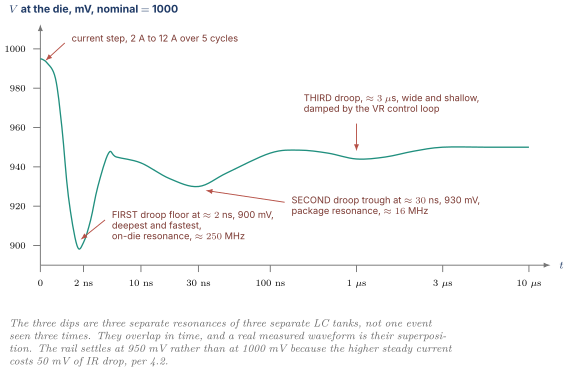
The interview-quality version of this is one sentence per tier. First droop is the on-die capacitance running out before the package can respond. Second droop is the package capacitance running out before the board can respond. Third droop is the board capacitance running out before the regulator's control loop can respond. Same failure at three scales, each one an order of magnitude slower than the last.
4.6 Why the consequence is a timing failure, and why nothing flags it
Tie it back to Part 1. Lower voltage means lower drive current means slower gates. From the frequency table in 1.2, at 0.90 V the logic can only sustain 0.909 of its nominal frequency. A 100 mV first droop therefore makes every path in the affected block about 10 percent slower for the duration.
Put the number on it. At 3.0 GHz the period is 333 ps. A critical path with 5 percent slack takes 316 ps at nominal voltage. Slow it 10 percent and it takes 348 ps, which is 15 ps longer than the period. Setup violation. And exactly as in 2.3 there is no signal, no exception, and no log entry. The captured bit is simply wrong and it propagates.
Two properties make droop-induced failures worse than the DVFS sequencing failure of 2.3. They are workload correlated, so the very code that causes the droop is the code running when the failure occurs, meaning failures cluster in vector kernels and cryptography loops and other high-activity code and are absent everywhere else. And they are self-concealing, because if the droop caused a wrong branch or a wrong load address, the machine goes off into different code, the activity pattern changes, the droop stops, and the failure signature evaporates.
That is why the topic gets its own discipline. And it is why the naive fix, described next, is so tempting and so expensive.
The naive fix is guardband. Set the nominal voltage 100 mV above what static timing requires, so that even at the bottom of the worst droop the logic still has enough. It works. It requires no new circuits, no detection, no response, and no verification of any dynamic mechanism. And from 3.2 it costs 27 percent of total power, on every cycle, forever, to survive an event with a duty cycle of a few parts per hundred thousand. Once you have said that sentence, everything in Part 5 justifies itself.
05.Part 5, mitigating droop
Five families of technique, and they attack different terms of the equation. Decap increases . Ramp control increases . Microarchitectural throttling decreases . Detection plus response reduces the duration of the excursion. Adaptive clocking does something categorically different and simply makes the droop harmless.
5.1 Decoupling capacitance, three tiers with three different jobs
A decoupling capacitor is a local reservoir of charge parked next to the load. Its only job is to supply current faster than the network above it can, for as long as it takes the network above it to catch up.
On-die decap is built from MOS capacitors, meaning transistors with source and drain tied together so the gate oxide is the dielectric, or from metal-insulator-metal capacitors between upper metal layers. It responds in picoseconds because it is microns from the load, and it handles first droop and nothing else. The cost is area, and it is not small. On-die decap density runs 10 to 20 fF per square micron, so the 200 nF in the worked example needs 10 to 20 square millimetres of dedicated capacitor, which on a large SoC is several percent of the die spent on structures that compute nothing. Designers recover part of it by filling post-placement gaps with decap filler cells, which is free because the space was empty, but the deliberate blocks are real silicon. There is a leakage penalty too, because a MOS capacitor is a thin gate oxide across the full supply and it tunnels.
Package decap is discrete ceramics on the package substrate, land side under the die or ringed around it. Responds in nanoseconds to tens of nanoseconds and handles second droop. Costs package area and assembly complexity rather than die area, which is why there is far more of it.
Board decap is bulk capacitance near the regulator, a mix of large ceramics and polymer or electrolytic parts. Responds in microseconds, handles third droop, and rides through until the regulator's control loop catches up. Cheapest per farad by orders of magnitude and useless for anything fast, because it is centimetres away and the intervening inductance dominates.
The rule that ties the tiers together is that each one must hold up the rail for exactly as long as the next tier out takes to respond, and no longer. Sizing on-die decap to cover a microsecond would require 100 uF on the die and is absurd. Sizing it to cover 2 ns is the actual requirement and is buildable. That is why the tiers exist, and it is the crisp answer to "why not put all the capacitance in one place".
One counterintuitive point that gets asked. Adding capacitance does not always help and can hurt. Every capacitor forms a resonance with the inductance in series with it, so adding capacitance at a badly chosen value moves a resonance rather than damping it, sometimes onto a frequency the workload actually excites. PDN design is impedance shaping, where the goal is a flat, low impedance across the whole frequency range rather than maximum capacitance, and that needs deliberate damping as well as farads. If the rail must stay within 50 mV at 25 A of transient, the target is milliohms flat from DC up to the fastest rate the current can change. Stating the problem as a flat target impedance rather than as an amount of capacitance is what a power integrity engineer would say.
5.2 Detecting a droop in a handful of nanoseconds
You cannot respond to what you cannot see, and from 2.4 you have single-digit nanoseconds to see it. Two detector families.
Ring oscillator droop monitors are small free-running rings powered from the local rail, whose oscillation frequency is a direct function of the supply, so counting edges over a short window measures the supply. Work the resolution. A 5 GHz ring over a 4 ns window produces 20 edges, and a 10 percent droop slows it to roughly 4.5 GHz, producing 18 edges in the same window. Two edges of difference is easily distinguished, so a 4 ns measurement window resolves a 10 percent droop, and a finer threshold needs only a slightly longer window or a faster ring. Total detection latency including the comparison is 5 to 10 ns. Cheap, all digital, tolerant of process variation because the threshold is calibrated per die, and easy to place in quantity.
Analog comparators compare the local rail directly against a bandgap-derived reference. Faster, sub-nanosecond, but they need an accurate reference distributed across the die, they are sensitive to noise coupling, and they are analog design in a digital flow.
Placement matters as much as the detector. Droop is local, because the on-die grid has resistance and a vector unit hammering its corner of the die droops harder than the fetch unit across the floorplan. A single monitor at the power pin sees almost nothing. Monitors go beside the blocks with the biggest current swings, which means beside the vector units and the large arrays, and a modern SoC has many.
5.3 Adaptive clocking, which is the elegant answer
Everything so far either prevents the droop or reacts by doing less work. Adaptive clocking does neither. It accepts the droop and changes the clock so that the droop stops mattering.
Start from the observation that made this possible. A droop is a timing failure only because the clock period stayed the same while the logic got slower. If the clock period stretched by exactly the same proportion that the logic slowed, then every path still fits inside its period, no setup constraint is violated, and not one instruction is discarded. The machine simply runs slightly slower for the few nanoseconds the droop lasts.
Work the numbers on the event from 4.4. Nominal is 1.00 V, 3.0 GHz, 333 ps period. The droop takes the rail to 0.90 V. From the frequency table in 1.2, at 0.90 V the logic supports 0.909 of nominal frequency, so it needs a period of ps. Stretch the clock from 333 ps to 366 ps for the duration and timing is met.
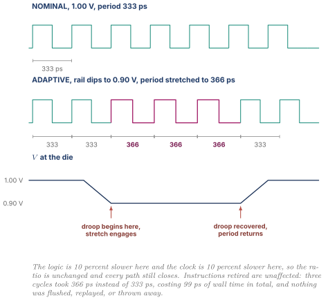
Two implementation families, and they differ in whether they need to detect anything at all.
Open-loop supply-tracking clock generation. Build the clock from a digitally controlled oscillator or a delay line powered by the same rail as the logic. When the rail dips, the oscillator slows by exactly the physics that slows the logic, with zero detection latency and zero control loop. This is the beautiful version. The difficulty is that the oscillator is not the critical path, so its voltage sensitivity only approximately matches the logic's, and you have to calibrate the match and keep residual margin for the mismatch. There is also a system problem, because a clock whose frequency wanders is no longer a stable time reference, which 5.4 returns to.
Closed-loop detect and stretch. Use the ring oscillator monitor of 5.2 to detect the droop, then stretch. The stretch itself is usually implemented as a phase interpolator or a programmable delay in the clock path that can insert a controlled fraction of a period, or in the crudest form as switching to a divided clock through a glitch-free mux per Clocking Reset and Domain Crossing. The cost is detection latency. You still need enough guardband to survive the first 5 to 10 ns unaided, so a closed-loop scheme recovers less margin than an open-loop one.
Three details that separate someone who has thought about this from someone who has read about it.
Stretching is safe for hold timing. A hold constraint is a race between the launch edge and the same capture edge, so it does not involve the clock period at all. Lengthening the period cannot create a hold violation. Setup gets strictly more time. So stretching is monotonically safe in both directions, which is precisely why it is preferable to any scheme that speeds a clock up.
The stretch must be applied at the root of the clock tree. If two branches of the tree stretch by different amounts, you have injected skew, and per section 6.2 of Digital Logic and Timing skew moves setup and hold in opposite directions and can break hold, which is unfixable at runtime. So the stretch happens once, before the tree, and the whole domain stretches together.
Everything outside the domain has to cope. A stretched clock breaks any fixed ratio to another domain's clock, so every interface out of the adaptive domain has to be asynchronous or bisynchronous, which is Clocking Reset and Domain Crossing again. It also breaks any counter that assumed a constant period, so cycle counters and performance counters measure cycles while wall-clock time must be measured from a separate always-on reference clock, and any code that converts cycles to seconds by multiplying by a constant becomes wrong. On a real machine this is why there is both a cycle counter and a constant-rate timer, and why they disagree.
5.4 Stretching versus throttling, priced
Both are legitimate. They cost different things and the comparison makes the argument for stretching concrete. Take the event of 4.4, a 100 mV droop lasting 20 cycles.
| Response | Correct? | Work lost in the event | Always-on cost | Response latency needed |
|---|---|---|---|---|
| Do nothing | no, setup violates | silent corruption | none | not applicable |
| Guardband to 1.10 V | yes | none | +33 percent power on every cycle forever | none |
| Throttle issue to zero for 20 cycles | yes | 20 cycles of issue | none | must react in a few ns |
| Delete one clock pulse in four for 20 cycles | yes | 5 cycles equivalent | none | must react in a few ns |
| Stretch the period 10 percent for 20 cycles | yes | 2 cycles equivalent | tiny, the stretch circuit | must react in a few ns, or zero if open-loop |
Check the stretch row. Twenty cycles at 366 ps instead of 333 ps is ps of extra wall time, and 660 ps divided by the 333 ps nominal period is 1.98, so two cycles equivalent. Compare the guardband row, , a 33 percent power tax paid continuously.
Stretching loses two cycles out of twenty. Throttling loses all twenty. Guardbanding loses a third of your power forever. That comparison is the whole argument, and it is the reason "we stretch instead of throttling" is the answer an interviewer is listening for. The deeper reason it is elegant is that stretching preserves work while throttling destroys it. Throttled cycles are cycles where the machine was correct but idle. Stretched cycles are cycles where the machine did its full work, just a little more slowly. Nothing is flushed, nothing is replayed, no speculative state is discarded, and no branch predictor or prefetcher state is disturbed.
The honest limits are worth volunteering. A stretch can only cover a droop the circuit can track, so a droop deeper than the design range still needs a hard throttle as a backstop. Stretching does not reduce the current draw, so it does not stop the droop, it only survives it, meaning a sustained heavy phase still needs the microarchitectural techniques of 5.6. And a stretch that persists for a long time is indistinguishable from running at a lower frequency, which is fine but means the performance counters need to be able to report it.
5.5 Current ramp control, attacking instead of
Go back to the arithmetic in 4.3. Nothing about it required to shrink. Stretching works exactly as well and it is often much cheaper.
The clearest case is power gating wake-up, which is the direct link back to section 6.3 of Power Fundamentals and Clock Gating. When sleep transistors turn on, the block's entire virtual rail and every capacitor inside it charges from zero. Turn the whole switch network on in one cycle and you can pull an amp or more for a few nanoseconds, which is a far worse than any workload transition. The fix is the daisy chain, where a small weak switch turns on first and the large ones follow through deliberately delayed buffers, spreading the inrush over hundreds of nanoseconds instead of a few.
Quantify the improvement. Say waking a block needs 1.5 A of inrush. Delivered over 5 ns, A/s, and through 100 pH that is 30 mV. Delivered over 500 ns, A/s, and through the same inductance that is 0.3 mV. A hundredfold slower ramp is a hundredfold smaller inductive droop. The only cost is that the wake takes 500 ns instead of 5 ns, which against the microsecond-scale break-even time computed in Power Fundamentals and Clock Gating is free.
The same idea generalises well beyond power gating. Bring a wide vector unit up lane by lane over several cycles instead of all at once. Enable the clock to a large array in stages. Stagger the wake-up of multiple cores in a cluster so that two blocks do not present their inrush to the same package inductance in the same nanosecond, which is a coordination problem across blocks and therefore lands squarely on the SoC power controller rather than on any single block's designer.
5.6 Microarchitectural techniques for power integrity
This is the exact phrase such roles use, and the reason the bullet sits under a microarchitect role rather than a circuits role is that everything in this section is a decision about how instructions are scheduled, not about how transistors are built. A circuits engineer can add decap and build a droop monitor. Only a microarchitect can decide that the machine will not issue four wide-vector operations in the same cycle immediately after an idle window.
Cap simultaneous wide issue. The current step in 4.4 came from four vector pipes going from idle to full width in five cycles. Restrict the scheduler so at most two of the four may accept a full-width operation in any cycle for the first N cycles after a low-activity window. Peak halves and the droop halves with it, at a bounded and small performance cost, because the pathological case is a cold start into a vector kernel and the restriction lifts after a few tens of cycles.
Ramp the issue width with a credit counter. Generalise the cap into a counter that starts small after an idle period and grows by one every few cycles until it reaches full width. That turns a step into a ramp, which from 5.5 is exactly what reduces , using a mechanism the scheduler in Out of Order Execution already has.
Insert deliberate low-activity cycles. After a droop monitor reports a large activity jump, force a bubble every k cycles for a fixed window. This is throttling and it is the blunt instrument, but as a backstop under adaptive clocking rather than the primary response it costs almost nothing because it fires rarely.
Break up a single wide operation. A 512-bit FMA can go to a 512-bit datapath in one cycle or to a 128-bit datapath over four. The four-cycle version has a quarter of the peak current for four times the duration. That is a real design point with performance consequences, and it is one reason a machine's vector width is a power decision and not only a throughput decision. See Execution Units and Vector Microarchitecture.
Avoid exciting a resonance, which is the non-obvious one. The second droop tier resonates at 16 MHz, which at 3 GHz is a period of cycles. Now picture a loop alternating 94 cycles of heavy vector work with 94 cycles of memory stall. That drives current at exactly the package resonant frequency, and each iteration adds to the ringing left from the previous one, the same way pushing a swing in time with its natural period builds amplitude. A pattern that would individually cause a 30 mV droop can build to 150 mV over several iterations. This is why "power virus" and "resonant workload" are real validation categories written deliberately, and why some designs detect a repeating activity pattern near a known resonance and dither it, perturbing the phase so the excitation stops adding coherently. Raising this unprompted is a strong signal, because it only makes sense once you have understood that the PDN is a resonant system and not just a resistor.
Coordinate across blocks. All of the above is per-core. Above it sits how many cores, the GPU, and the neural engine may ramp in the same instant while sharing one package inductance. That is a global arbitration problem and it belongs to the SoC power controller, which is to say the Resource Controller.
06.Part 6, thermal
6.1 Power becomes heat, and the model is an RC circuit
Every watt a chip consumes leaves as heat. There is no other exit. So a steady-state temperature is set by a simple relation that looks exactly like Ohm's law with temperature standing in for voltage and power for current.
is the thermal resistance in degrees Celsius per watt, and it is the sum of everything between the transistors and the outside air. Silicon to package, package to heatspreader, heatspreader through thermal interface material to a heatsink or to the chassis, and finally to air. Work one. A laptop SoC dissipating 25 W with a total junction-to-ambient thermal resistance of 1.5 C/W in a 30 C room sits at C. Double the power to 50 W and it sits at 105 C, which is at or past the limit.
Add capacitance and the model becomes an RC circuit, which is what gives thermal its time constants. The thermal capacitance is how many joules raise something by one degree, and is the time constant. Work the die. Silicon has a specific heat around 700 J/(kg K) and a density of 2330 kg/m³, so a 100 mm² die 0.5 mm thick has a volume of m³, a mass of kg, and
Now the number that sets everything. With 10 W going in and, for an instant, no heat leaving,
The die heats at 122 degrees per second when unopposed, which is 0.12 C per millisecond, so a control loop sampling at one kilohertz sees at most a tenth of a degree between samples and that is comfortable. A local hot spot is worse. Scale the calculation down to a 1 mm² spot in a vector unit dissipating 0.5 W and falls to about J/K, giving 610 C per second, or 0.6 C per millisecond. Lateral spreading in the silicon fights this, but it is why hot spots need faster attention than die averages and why sensor placement in 6.5 matters.
The chassis is at the other extreme. A 150 g aluminium phone frame at 900 J/(kg K) has J/K, so absorbing 4 W above sustainable for one minute stores 240 J and raises the frame C. Tens of seconds of burst before the outside of the phone warms noticeably, which is the physical basis of a turbo window.
6.2 The three effects of temperature
Transistors get slower. Carrier mobility falls as temperature rises because lattice vibrations scatter carriers more. Delay increases roughly 0.1 to 0.3 percent per degree, so a swing from 25 C to 100 C is 8 to 20 percent more delay. This is why timing signoff runs a hot corner, and it is part of the guardband stack in 3.1. It is also why an under-cooled chip fails at a frequency it passed at on the bench. Confusingly, at low supply voltages the effect can invert, because threshold voltage also falls with temperature and at low the threshold effect dominates the mobility effect, so a device gets faster when hot. That is temperature inversion and it is why modern signoff has to check a cold corner as well.
Leakage rises exponentially. From 1.4 of Power Fundamentals and Clock Gating, subthreshold current has an exponential temperature dependence, roughly doubling every 10 degrees, and a conservative factor of 1.7 per 10 degrees is the number used there. This is the dangerous one and 6.3 develops it.
Wearout accelerates. Electromigration, where current gradually pushes metal atoms along a wire until it opens or shorts, has an Arrhenius dependence on temperature. Bias temperature instability, where the threshold voltage drifts over years of operation, likewise. A rough rule from reliability physics is that a 10 degree rise halves lifetime. That converts a thermal limit from a performance question into a warranty question, and it is why the limit is enforced by hardware and cannot be overridden by software.
6.3 Thermal runaway, worked until it diverges
Take the second effect seriously and you get a positive feedback loop.
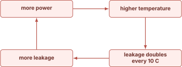
Whether that loop is stable is not obvious and it is not a property of the chip alone. Work it. Take a block with 10 W of dynamic power that is fixed and independent of temperature, plus leakage that is 3 W at 50 C and scales by a factor of 1.7 per 10 degrees, so . Ambient is 40 C. Solve by iterating.
First with a poor cooling solution, C/W.
| Step | in | out | ||
|---|---|---|---|---|
| 1 | 66 C | 7.0 W | 17.0 W | 74 C |
| 2 | 74 C | 10.7 W | 20.7 W | 81 C |
| 3 | 81 C | 15.9 W | 25.9 W | 92 C |
| 4 | 92 C | 27.6 W | 37.6 W | 115 C |
| 5 | 115 C | 95 W | 105 W | 250 C |
It diverges. There is no equilibrium. The part destroys itself.
Now the identical die with a good cooling solution, C/W.
| Step | in | out | ||
|---|---|---|---|---|
| 1 | 46.5 C | 2.49 W | 12.49 W | 46.2 C |
| 2 | 46.2 C | 2.45 W | 12.45 W | 46.2 C |
It converges immediately, to 46 C. Same silicon, same workload, same leakage physics. The only thing that changed was the thermal resistance, and one case is stable and the other destroys the part.
The condition separating them is a loop gain. The loop is stable when
Evaluate both cases. Since , the derivative is per degree. In the good case, W so W/C, and , comfortably below 1. In the bad case at 92 C, W so W/C, and , above 1 and diverging. The criterion is exact and the arithmetic is checkable, which is why this is worth working out rather than asserting.
Two conclusions follow and both are important. Thermal management is a safety mechanism, not an optimization. A DVFS controller that fails to lower the operating point does not merely underperform, it lets the loop go unstable and destroys the part, so the thermal path in a power controller has to be independent of the performance path, has to be fail-safe, and typically has a hardware backstop that fires without any firmware involvement. And the loop gain rises with temperature, because is itself proportional to , so a system that is stable at 60 C can be unstable at 100 C. The margin is not uniform, and that is why thermal limits are hard walls rather than soft targets.
6.4 TDP, and why peak power exceeds it
Thermal design power is the sustained power the cooling solution is designed to remove while holding the junction below its limit. It is a cooling specification, not a chip specification, and confusing the two is common.
| Platform | Cooling | Sustained TDP | Short-burst peak | Why the gap exists |
|---|---|---|---|---|
| Phone SoC | passive, chassis is the heatsink | 3 to 5 W | 8 to 12 W for tens of seconds | 135 J/K of chassis thermal mass |
| Tablet | passive, larger chassis | 6 to 10 W | 15 W | more mass, more surface area |
| Fanless laptop | passive, larger still | 10 to 15 W | 30 W briefly | more mass again |
| Fan-cooled laptop | active | 25 to 45 W | 60 W or more | heatsink mass plus fan ramp lag |
| Desktop | large heatsink or liquid | 65 to 250 W | modest headroom | already near steady state |
The peak column exists entirely because of thermal capacitance. From 6.1, absorbing 4 W above sustainable for 60 s raises a phone chassis by 1.8 C, so a burst is genuinely free until the accumulated energy shows up as temperature. Turbo is the deliberate exploitation of thermal mass, and its duration is set by whichever thermal tier saturates first. The die saturates in milliseconds, the heatspreader in seconds, the chassis in a minute or more, so a real turbo policy is a stack of budgets on different time windows rather than one number, and a controller typically tracks several exponentially-weighted moving averages of power at different time constants and throttles when any of them exceeds its own limit.
Skin temperature is the constraint that actually binds on a phone. Regulatory and comfort limits put the outside surface of a handheld at roughly 43 C, and that is reached long before the junction limit of 100 to 110 C. A phone therefore throttles because of the outside of the device, a laptop throttles for a mix of junction limit and fan noise, and a desktop throttles for junction limit alone. The consequence is that a phone SoC's sustained performance is set by industrial design and materials rather than by silicon, which is non-obvious and worth saying.
6.5 Sensors, and the problem with where they are
Two sensor technologies. Analog thermal diodes, using the fact that a forward-biased junction's voltage falls predictably with temperature at about 2 mV per degree, which is accurate but needs an ADC and analog routing. Digital ring-oscillator sensors, using the fact that oscillator frequency falls with temperature, which is all digital, easy to place anywhere, and less accurate absolutely but perfectly adequate relatively once calibrated per die at test.
The interesting problem is not the sensor, it is the placement. A modern SoC has tens of sensors and still cannot see the true peak, for three reasons. The hot spot is smaller than the sensor spacing, since the genuinely hottest point might be a few hundred microns across inside a vector unit or a high-activity array, and a sensor 500 microns away reads lower because lateral spreading diffuses the gradient. The sensor lags, because heat diffusing a millimetre through silicon takes hundreds of microseconds to milliseconds, so the reading describes the temperature the hot spot had a moment ago. And the offset is workload dependent, because how much lower and how much later depends on which block is hot, which depends on what code is running, so a fixed calibration offset is wrong for some workloads.
The practical responses are to place sensors deliberately beside the known hot blocks rather than on a uniform grid, to add more of them, to estimate the true hot spot from sensor readings plus performance counters through an activity-weighted model rather than trusting the readings alone, and to keep margin for the residual error. That last one is another guardband, and like every guardband it costs performance, so better sensing pays.
6.6 The throttle escalation ladder
A thermal controller does not have one response, it has a graded set, ordered from cheapest to most drastic. Each rung is entered when the rung below it fails to arrest the rise, and each has hysteresis so the machine does not oscillate.
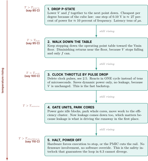
Two things are worth saying about the ordering. Rung 1 comes first because the cube law makes it by far the most efficient response, buying 27 percent of power for 10 percent of frequency. Rung 3 exists despite being less efficient purely because it is fast, responding in one cycle where a P-state change takes tens of microseconds, and in an emergency latency beats efficiency. And rung 5 must be implemented in hardware with no software in the path, because the whole point is that it still works when the firmware has hung.
6.7 Race to idle, including when it loses
Race to idle says that finishing a job quickly at high power and then dropping into a deep sleep state uses less total energy than running slowly for longer, because the fixed overheads of being awake are paid for less time. It is repeated constantly as if it were always true. It is not, and knowing exactly when it fails is the point of this section.
Set up the comparison carefully. A job of 1 billion cycles, and a platform overhead that is paid the whole time the machine is awake, covering always-on logic leakage, DRAM in an active state, the PMIC's own quiescent draw, the display pipeline, and everything else that cannot sleep while the CPU is running.
| Race, P1 | Crawl, P4 | |
|---|---|---|
| Operating point | 1.00 V, 3.0 GHz | 0.60 V, 1.66 GHz |
| Core power, from | 5.00 W | W |
| Time for cycles | 0.333 s | 0.602 s |
| Core energy | 1.67 J | 0.60 J |
| Platform energy at |
Now evaluate at two different platform overheads.
With W, a well-designed system with an aggressive sleep architecture, racing costs J and crawling costs J. Crawling wins by 30 percent.
With W, say a laptop with the display on and memory active, racing costs J and crawling costs J. Racing wins by 13 percent.
Find the crossover exactly. Racing saves s of awake time and costs J of extra core energy, so racing wins when
About 4 W of platform overhead is the break-even. Below it, crawl. Above it, race. That is a real, derivable answer, and it is far better than "it depends".
Four more conditions flip the answer, each worth naming. The sleep state has to be deep and reachable, because racing only pays if the machine actually enters a state where the overhead goes away, and if the deepest available state still burns 3 W because a peripheral holds a wake lock then racing bought nothing. Entry and exit energy has to be amortised, since from section 6.3 of Power Fundamentals and Clock Gating power gating costs a fixed energy with a break-even idle time of microseconds, so waking for 1 ms every 10 ms amortises easily while waking for 5 us every 20 us does not. The fast point has to be thermally sustainable, because if racing pushes the die into the throttle ladder of 6.6 you end up at the crawl point anyway, having paid the transition costs for nothing. And memory-bound work does not race, because if the job is waiting on DRAM then doubling core frequency barely changes runtime, so you paid the cube-law premium and got almost no time back. That last one is the most common practical failure, and it is why a good governor looks at stall counters and instructions per cycle rather than only busy fraction, which connects to the modelling in Performance Modeling.
Race-to-idle is therefore a conditional result, and its conditions are a large platform overhead, a deep and cheap sleep state, thermal headroom, and a compute-bound workload. Saying "it depends on whether the platform overhead exceeds roughly four watts, and here is the arithmetic" is far stronger than either repeating the slogan or dismissing it.
07.Part 8, check yourself
Answer out loud, in full sentences, as if an interviewer had asked. If you cannot, reread the section named.
- Derive why power scales with the cube of voltage. Start from the delay model and show why is roughly linear in , then say why the naive quadratic answer is incomplete. (1.2, 1.3)
- Cut the supply 20 percent. What happens to power, and separately what happens to energy per operation, and why are those two different numbers? (1.3, 1.4)
- Name three separate floors that stop you from lowering voltage indefinitely, and say which one usually binds first in a real design. (1.5)
- Give the correct order for moving to a faster operating point, draw the voltage-frequency plane, and name the forbidden corner. Then say exactly what failure occurs if you reverse the order and why it is worse than a crash. (2.2, 2.3)
- A regulator step takes tens of microseconds and a first droop is over in a few nanoseconds. What does that fact rule out, and what does it force you to build instead? (2.4)
- You need to change frequency in under a microsecond and a PLL relock takes fifty. Give three ways out and say what each costs. (2.5)
- Enumerate the components of the voltage guardband and price the whole stack using the cube law. Compare that number against what an aggressive clock gating campaign saves. (3.1, 3.2)
- What does adaptive voltage scaling measure, what are the three sensor options, and what is the honest weakness of a critical path replica? Then say why AVS cannot help with droop. (3.3)
- An LDO converts 1.8 V to 0.9 V at 5 A. How much power is wasted, and why would you ever use one? (3.5)
- Write the droop equation and explain both terms physically. Then work the number for a 10 A step in five cycles through 100 pH, and then work the actual droop with 200 nF of on-die decap, and explain why the two answers differ by a factor of six. (4.2, 4.3)
- What are first, second, and third droop? Give the physical origin, the rough resonant frequency, and the response time of each, and explain why the frequency rises as you get closer to the die. (4.5)
- Explain adaptive clocking. Why does stretching the clock preserve work where throttling destroys it, why is stretching always safe for hold timing, why must the stretch be applied at the root of the clock tree, and what does it break outside the domain? (5.3, 5.4)
- Give four microarchitectural techniques for power integrity, and explain the resonant-workload case including why a repeating pattern can build a droop far deeper than a single burst would. (5.6)
- Work thermal runaway as a feedback loop with real numbers, show the same die diverging with one cooling solution and converging with another, and state the stability criterion. Then say why that makes thermal management a safety mechanism rather than an optimization. (6.3)
- When does race-to-idle lose? Derive the break-even platform overhead, and name three other conditions that flip the answer. (6.7)
08.Part 9, related notes
- Power Fundamentals and Clock Gating for the dynamic power equation this note builds on, for leakage and its temperature dependence, and for the power gating wake-up that 5.5 attacks as a di/dt source
- Digital Logic and Timing for the delay model behind the frequency-voltage relationship in 1.2, and for the setup and hold analysis behind 2.3 and the root-stretch rule in 5.3
- Clocking Reset and Domain Crossing for PLL relock latency, glitch-free clock muxing, and the asynchronous crossings that per-domain scaling and adaptive clocking both force on you
- SRAM Arrays and ECC for the array Vmin floor that sets the bottom of the operating point table in 2.1
- Execution Units for the vector pipes whose issue ramp is the current step in 4.3, and for the width-versus-cycles tradeoff in 5.6
- Out of Order Execution for the scheduler that issue throttling modifies, and for why per-instruction energy is dominated by the machinery around the ALU
- STA Synthesis and Physical Design for the corners, derates, and OCV pessimism in the guardband table of 3.1, and for IR-aware timing signoff
- DFT and Silicon Debug for on-die monitor infrastructure, per-die calibration at test, and the shmoo plots that characterize the operating point table
- Verification Methodology for where the DVFS sequencing state machine gets verified and why formal is the right tool for the ordering property in 2.3
- Performance Modeling for the stall-versus-compute analysis that decides whether race-to-idle applies to a workload
- Power, Frequency, and Thermal for the vault's architectural treatment of DVFS, race-to-idle, dark silicon, thermal throttling, and turbo
- Trends, Constraints, and Quantitative Principles for Dennard scaling and why frequency growth stopped
- Case Study: ARM Cortex-X3 and Neoverse N2 for a real core's published power management structure