Reliability, Aging, Variation, and Silicon Lifetime
September 8, 202639 min readadvanced
"Reliability" in a job description covers three questions with nothing physically in common. They fail differently, they are found by different tools, and they are fixed at different points in the schedule.
01.Part 1, the three questions reliability asks
1.1 One word, three unrelated questions
"Reliability" in a job description covers three questions with nothing physically in common. They fail differently, they are found by different tools, and they are fixed at different points in the schedule.
Does this particular die work at all, right now. A wafer comes out of the fab with particles, misaligned layers, and metal bridges, so some dies are simply broken. Finding them is testing, the subject of DFT and Silicon Debug, and the commercial measure is yield.
Does it work under every condition it will ever see. Not at 25 degrees on a bench, but at 110 degrees, at the bottom of a supply droop, on a die from the slow edge of the wafer. This is variation and margin, Part 2, and the failure is not that the chip is broken but that your analysis was wrong about what it would survive.
Will it still work in five years. A chip that passes every test on day one can fail on day 900. Transistors get slower as they are used, wires erode as current flows, and gate insulators eventually puncture. This is aging and wearout, Part 3, and none of it is visible at test.
A fourth thing gets filed under reliability and behaves unlike all three. A cosmic ray secondary flips a bit in your cache. Nothing broke and nothing degraded, and rewriting the location makes it perfect. That is a soft error, Part 4, and confusing it with aging is a common stumble because both look like "the chip went wrong after working fine for a while."
1.2 Why the split changes the answer
| Question | Failure is | Found by | Fixed by |
|---|---|---|---|
| works at time zero | permanent, present at birth | scan, ATPG, BIST, wafer sort | screening, redundancy, repair |
| works at all conditions | not a failure, an analysis gap | multi-corner STA, IR drop, EM analysis | margin, corner coverage, adaptive circuits |
| works in five years | permanent, arrives late | aging-aware STA, burn-in, field data | guardband, current density rules, thermal design |
| soft errors | transient, no damage | statistical modelling, beam testing | ECC, parity, replay, architectural triage |
The line that shows you hold the split is that the first three are the chip being wrong and the fourth is the chip being right and the data being wrong. A soft error is a correct machine executing on corrupted state.
Four words get used loosely. A defect is a physical imperfection, a fault is its logical model such as "stuck at 0", an error is a wrong value in state, and a failure is that error becoming visible. Most defects never become failures, because they land somewhere unused or their error is masked, which is why derating exists in Part 4.
02.Part 2, process variation, from first principles
2.1 Count the dopant atoms and the mystery dissolves
A transistor's threshold voltage is set partly by how many dopant atoms, impurity atoms implanted to set the silicon's electrical behavior, sit in the channel.
Take a planar transistor with a channel roughly 20 nm on a side. Doping is quoted per cubic centimetre, and cm, so the channel volume is cm. At a channel doping of atoms per cubic centimetre,
Eight atoms. Not eight million. Implantation places atoms independently at random, so the count is Poisson with standard deviation . A transistor drawn with 8 dopants has 8 plus or minus about 3, a 35 percent swing in the quantity setting its threshold, in a perfect fab.
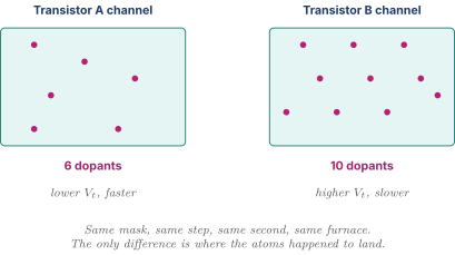
That is random dopant fluctuation, RDF, the largest contributor to threshold mismatch in planar CMOS. Pelgrom's law makes the spread inversely proportional to the square root of device area, . With mVm and m, mV. Against a nominal of 400 mV a three-sigma device is off by 225 mV, and since leakage changes tenfold per 78 mV of threshold shift from Power Fundamentals and Clock Gating, a three-sigma-low device leaks roughly times more than a three-sigma-high one. These are illustrative public-literature magnitudes rather than any vendor's numbers.
Smaller devices vary more, which is why SRAM and analog designers upsize critical devices, and the 6T SRAM cell, built from the smallest transistors on the die, is the most variation-sensitive structure there is. That is the deep reason behind the read stability versus write margin conflict in SRAM Arrays and ECC and the voltage floor limiting DVFS in DVFS Droop and Thermal. A FinFET channel is largely undoped, so removing the dopants removes the dominant randomness, and cutting variation was a stated motivation for that transition.
Two related sources round it out. Line edge roughness is a gate edge drawn straight printing wobbly, because photoresist is polymer molecules of finite size, and at a 20 nm gate a 1 to 2 nm wobble is a 5 to 10 percent variation in effective channel length. Gate oxide thickness variation is quantization, since a dielectric a few atomic layers thick cannot have half a layer. All three are atomic-scale discreteness showing through in a device only a few tens of atoms across.
2.2 Systematic versus random
Systematic variation is predictable from position and surroundings. Lithographic focus varies across the exposure field, polishing removes more material where metal density is high, and etch rate depends on surrounding open area so an isolated gate etches unlike one in a dense array. The defining property is that it is a function of location and layout context, so it repeats, which makes it addressable by rules such as dummy fill, single-orientation poly, and optical proximity correction that pre-distorts the mask so the printed shape comes out right.
Random variation has no such handle. RDF, line edge roughness, and oxide quantization are statistical, and knowing everything about a device's neighbours tells you nothing about which way it went. The two respond to opposite strategies. Systematic variation yields to discipline, random variation only to device size or margin.
2.3 Die-to-die versus within-die, and why the second is the hard one
Die-to-die variation shifts a whole die together, so every transistor on it runs a bit fast or a bit slow, caused by anything varying wafer to wafer such as furnace drift or implant dose calibration. Within-die variation is the difference between two devices on the same die, and RDF is entirely within-die.
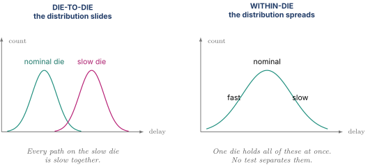
Die-to-die variation is commercially cheap and within-die variation is expensive, even though die-to-die variation is usually larger. The intuitive answer, that the bigger variation must be the worse problem, is wrong. Die-to-die variation is measurable per die and therefore sortable, so a slow die is not scrap but a lower-frequency product, and the variation gets monetized rather than paid for. Within-die variation cannot be sorted, because it lives inside every die including the good ones, and no test lets you sell path A separately from path B. Put a number on it. A 300 ps critical path at a 333 ps cycle, with within-die effects giving a standard deviation of 3 percent, means ps, so two paths on one die can sit at and , a 36 ps spread, close to 11 percent of the cycle, gone before the design does anything with it.
2.4 What STA does about it, and why statistics recovers real margin
STA Synthesis and Physical Design introduces on-chip variation. The simple form is a blanket derate, multiplying launch-path cell delays by 1.10 and capture-path delays by 0.90 so the check is guaranteed pessimistic.
A launch path has 10 stages of 30 ps each, 300 ps total, and each stage individually has a three-sigma spread of 10 percent, so ps. Blanket derate adds ps, silently assuming all ten stages hit their individual worst at once. Statistical treatment notices they vary independently, so variances add rather than standard deviations,
so three sigma on the path is 9.5 ps, not 30 ps. The blanket derate over-charged by 20.5 ps, over 6 percent of the cycle, because the probability of all ten stages simultaneously at three-sigma worst is roughly .
Blanket derate grows as , statistical margin grows as , so the correct derate gets smaller as the path gets longer, which is why advanced OCV tables are indexed by logic depth and physical distance. Recovering that pessimism is not accounting, since fake margin is bought back with upsized cells, extra buffers, or a lower frequency, each costing area and power on every path.
2.5 Binning, the commercial answer to die-to-die variation
Measure each die and sell it as what it is. Take a lot whose maximum stable frequency is normal with mean 3.2 GHz and standard deviation 0.15 GHz.
| Bin | Criterion | range | Fraction | Becomes |
|---|---|---|---|---|
| Top | above 3.4 GHz | 9.2 percent | highest price part | |
| Middle | 3.1 to 3.4 GHz | to | 65.7 percent | volume part |
| Low | 2.8 to 3.1 GHz | to | 24.8 percent | value or fanless part |
| Scrap | below 2.8 GHz | 0.4 percent | discarded or salvaged |
Same mask set, same wafer, same manufacturing cost, three prices. Binning is also multi-dimensional, since dies are sorted on leakage too, so a part can be rejected for being too fast in the wrong way, and it composes with repair, since a die with one bad cache way ships with that way disabled. Binning handles die-to-die variation completely and within-die variation not at all.
03.Part 3, aging and wearout, mechanism by mechanism
Everything in Part 2 is present on day one. Everything here arrives later, and no factory test could have caught it, because at the factory the part was genuinely fine.
3.1 Bias temperature instability, the one that makes transistors slower
Hold a PMOS gate at a negative voltage relative to its source, meaning the device is on, at elevated temperature, for a long time. Its threshold voltage magnitude increases, so it supplies less current and gets slower.
The physical picture. The silicon-to-oxide interface has dangling bonds passivated with hydrogen during manufacture. Electrical stress plus heat breaks some of them, the freed hydrogen drifts away, and the interface trap left behind holds charge, which shifts the threshold. This is NBTI in PMOS. The NMOS counterpart is PBTI, minor with silicon dioxide and significant with high-k metal gate stacks because the high-k layer traps electrons readily, so say BTI unless you mean one specifically. Two properties make BTI behave unlike anything else. It is sublinear in time, following with . Suppose a device drifts 25 mV over ten years. The one-year value follows from the ratio , giving mV, so year one did 17 mV and the following nine years added 8 mV. Damage front-loads heavily, which is why a device surviving early life tends to keep surviving. It also partially recovers, since removing the stress lets some charge de-trap, so a toggling transistor recovers between stress intervals and a statically-on one does not.
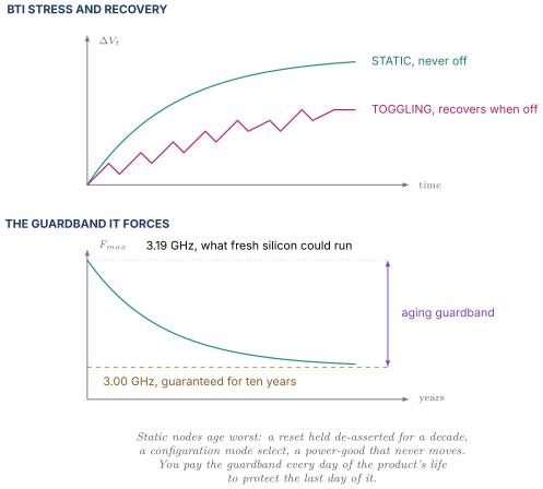
BTI slows the chip over its life, so a design that barely passes timing on day one fails in year three, and the response is an aging guardband, signing off against degraded libraries so the frequency still holds at end of life. Gate delay depends on overdrive as roughly with . Take V and V, so overdrive is 0.55 V, and the 25 mV drift takes it to 0.525 V,
about 6 percent slower at end of life. To guarantee 3.0 GHz for ten years you close timing 6 percent tight, so fresh silicon could have run at GHz. You pay the guardband every day of the product's life to protect the last day of it. That motivates on-die aging sensors and critical-path replica monitors, which would let a chip ship at 3.19 GHz and back off only as it actually degrades.
3.2 Hot carrier injection
A carrier crossing from source to drain is accelerated by the lateral field, and near the drain where the field peaks some become hot, far out of thermal equilibrium. A hot carrier hitting the interface can break a bond or lodge in the oxide, degrading drive current.
Two features distinguish HCI from BTI. It is driven by switching, not static bias, since damage accrues during the transition while the device carries current with a large drain-to-source voltage across it, so it scales with toggle rate and frequency and is a clock tree problem rather than a configuration logic problem. And it is worse at low temperature, because mobility rises as temperature falls, so carriers accelerate further between collisions and arrive hotter. So no single corner is worst-case. BTI, TDDB, and electromigration argue for a hot corner and HCI argues for a cold one, and lifetime signoff checks both ends.
3.3 Time dependent dielectric breakdown, the hard failure
BTI and HCI degrade gradually. TDDB does not degrade at all until it kills the transistor.
The gate oxide is an insulator a few atomic layers thick with the full supply across it. With 0.9 V across 1.5 nm the field is V per metre, 6 megavolts per centimetre, and any everyday insulator would have exploded. Under that field defects nucleate at random positions with nothing measurable happening, and when enough line up into a conducting path from gate to channel the oxide breaks down and a permanent short appears. A hard failure with no warning and no recovery.
The voltage dependence is brutal, with lifetime falling roughly as . A representative published figure is that roughly 100 mV of extra supply cuts oxide lifetime by about an order of magnitude, so a part designed for ten years at 0.9 V, run at 1.0 V, has an oxide lifetime near one year, and near a month at 1.1 V. That is why there is a hard in a DVFS table, and it is a much better answer than "because it gets hot". Frequency scaling in DVFS Droop and Thermal wants voltage as high as the thermal budget allows, and TDDB imposes a ceiling unrelated to temperature or power.
3.4 Electromigration, where the metal physically moves
The previous three damage transistors. This one damages wires, and it constrains things visible in a layout.
Current in a wire is electrons moving, and those electrons collide with the metal's own atoms and transfer momentum. One collision does nothing. Enough collisions over enough time and metal atoms are pushed along in the direction of electron flow, the electron wind. Atoms leave one region, thinning the wire until it opens, and pile up in another as a hillock that can short to a neighbour.
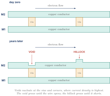
The model is Black's equation, , where is current density in amperes per unit cross-sectional area and is about 2, so halving current density multiplies lifetime by four.
Make current density concrete. A minimum-width wire on a lower metal layer, 40 nm wide and 80 nm tall, has m, which is cm. Design rules typically cap copper near 1 MA per square centimetre at operating temperature, so A. Thirty-two microamps in one minimum wire. Compare against a clock buffer from Power Fundamentals and Clock Gating driving 300 fF at 3 GHz and 0.9 V,
Twenty-five times the single-wire limit. That net needs twenty-five minimum widths of metal, or fewer wide wires on a thicker upper layer, or the buffer split into distributed smaller ones. The same arithmetic applies to the vias feeding it, whose cross-sections are smaller than the wires they join, which is why layout rules demand via arrays and double vias on high-current nets.
Three points separate reading about EM from signing it off. Signal nets and power nets are checked differently, since a power grid carries unidirectional DC so atoms move one way and never return, limited on average current, while a signal net swings both ways so some material moves back, the self-healing effect, limited on RMS current. The clock tree is the worst signal case, because it has by definition and toggles every cycle with no averaging down. And temperature enters through the exponential, so an EM-marginal net inside a hot spot fails far sooner than the same net in a cool region.
Two related mechanisms deserve a sentence each. Stress migration is metal atoms moving under a mechanical stress gradient rather than an electrical one, since copper and the surrounding dielectric have different expansion coefficients, and it needs no current at all. Thermal cycling is fatigue from repeated heating and cooling flexing the package until something cracks, driven by the number and depth of cycles rather than hours of operation, so a device power-cycled constantly can fail sooner than one left running.
3.5 Arrhenius, and why "double per ten degrees" is not a slogan
Every mechanism above except HCI accelerates with temperature through a rate proportional to , with eV per kelvin. Derive the rule rather than repeating it, taking eV and comparing 350 K with 360 K.
Here K and , so the exponent is and .
Roughly double per ten degrees, derived, and it depends on , so a higher-activation-energy mechanism accelerates faster. From 60 to 100 degrees is four steps, a factor of , so a part lasting ten years at 60 degrees lasts about nine months at 100 degrees. That closes a loop with the thermal runaway of Power Fundamentals and Clock Gating and DVFS Droop and Thermal. Higher temperature roughly doubles leakage per 10 degrees, leakage becomes heat, and heat raises temperature, which is the electrical runaway loop running in milliseconds and handled by throttling. The same temperature roughly doubles BTI, TDDB, and EM rates, which is the same physics on a timescale of years, handled by guardband and thermal design instead.
04.Part 4, soft errors, which are not aging at all
4.1 What actually happens, in charge, and where the particles come from
A particle passing through silicon leaves a track of electron-hole pairs. If that track passes near a reverse-biased junction the depletion field sweeps the charge to the node, which for a few tens of picoseconds receives an injected current it never asked for. Enough charge and the node's value flips.
How much charge does a node hold? The critical charge is the smallest injected charge that flips the node, and to first order it is the stored charge . For a small SRAM internal node with fF at V, fC, which in electrons is . Five thousand electrons is the entire margin between a stored 1 and a stored 0.
How much charge does a particle deposit? Silicon needs about 3.6 eV per electron-hole pair, so a 5 MeV alpha creates pairs, about 220 fC, spread along a track roughly 25 micrometres long. Only charge within about a micrometre of the junction is collected efficiently, so the collected charge is a few femtocoulombs. A few femtocoulombs arriving at a node whose entire margin is 0.8 fC. That comparison answers "why are soft errors a problem" far better than saying particles are energetic.
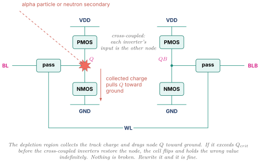
Two sources supply the particles. Alpha particles from package materials come from trace uranium and thorium in solder, mould compound, and ceramics, originating millimetres from the die, so this is a packaging problem addressed by low-alpha materials and purified solder. Neutron-induced secondaries from cosmic rays are the other, where an uncharged neutron deposits nothing directly but collides with a silicon or oxygen nucleus, and the resulting nuclear recoil products are heavy charged fragments depositing charge densely along a short track. Neutrons cannot be shielded practically, since stopping them takes metres of concrete rather than a lid, and the flux rises strongly with altitude, with published figures putting Denver at three to four times sea level.
4.2 FIT, defined and then made alarming
The unit is the FIT, failures in time, defined as one failure per device-hours. Suppose a design has a raw rate of 2000 FIT. For one device, hours, which is years. That sounds like the end of the discussion. It is not. Now ship ten million of them. A fleet of devices accumulates device-hours every wall-clock hour, so
Twenty an hour. 480 per day, about 175,000 per year. The number reading as a 57-year MTBF for one person is a permanent stream of support tickets for a product line. Run it backwards. To tolerate one field failure per day across the fleet,
About four FIT per chip, three orders of magnitude below where we started. Every ECC decision in the design is downstream of that gap.
4.3 Why SRAM dominates
Soft error rate scales with the number of sensitive nodes and how easily each is upset, and SRAM has by far the most nodes and the weakest ones, since the 6T cell uses the smallest devices in the library and its internal nodes carry the least charge on the die.
Figures on the order of 100 to 500 FIT per megabit are commonly cited for unprotected SRAM at sea level. Take 200 FIT per megabit and an 8 megabyte L2, which is 64 megabits, giving FIT. Against the 4 FIT budget from 4.2, that is a factor of 3200 too large from one array. That is the entire argument for ECC in SRAM Arrays and ECC, since ECC on large arrays is not a robustness nicety but the only way the product exists. SECDED corrects every single-bit error, collapsing the residual to the rate of double-bit errors within one protected word, and scrubbing stops single-bit errors accumulating into double-bit ones. Flip-flops matter less, both because there are far fewer of them and because a flop node holds more charge.
4.4 Three failure types with three different names
A single event upset, SEU, is a stored bit flipping, so a cell or flip-flop holds the wrong value until something overwrites it. A single event transient, SET, is a glitch on a combinational node, where the strike injects charge, the node produces a wrong voltage for tens of picoseconds, and the wrong value propagates. If it arrives at a flip-flop's input during that flop's setup and hold window it gets captured and becomes an SEU. Otherwise the node recovers and nothing happened.
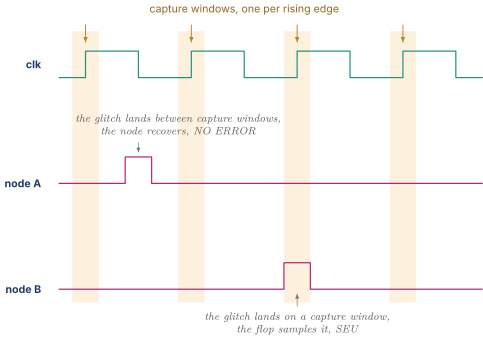
That diagram contains the reason SET-induced errors rise with frequency. The number of capture windows per second is the clock frequency, so the vulnerable fraction of time grows as the period shrinks. This is temporal masking, one of three, alongside logical masking, where the glitch reaches a gate whose other input makes it irrelevant, and electrical masking, where the glitch attenuates through gates that cannot pass a pulse narrower than their own response time.
A multi-bit upset, MBU, is one particle flipping two or more adjacent cells, since as cells shrink a single track can pass near several. This matters enormously, because SECDED protects one error per word and two in a word is exactly what it cannot correct. The defence is physical bit interleaving, laying out the array so bit 0 of eight different words sits together rather than bits 0 through 7 of one word, so a strike flipping four adjacent cells produces four single-bit errors in four different words. That is why array column multiplexing and ECC word organization are designed together.
4.5 Scaling, and the derating that keeps this from being hopeless
Two opposing effects run as cells shrink. Charge falls, since and both shrink, so going from fF at 1.0 V to fF at 0.7 V takes from 2 fC to 0.35 fC, about six times easier to flip. The target shrinks too, since halving linear dimensions cuts the cross-section presented to a randomly directed particle by four. The net is that published per-bit rates have been roughly flat to declining across recent generations while per-chip rates keep rising, because the per-device physics got a little better and the integration got a lot bigger.
Now the derating that stops 12,800 FIT from describing reality. Most upsets never become failures, because a flipped bit only matters if the wrong value is actually read and used in a way that reaches the outside world. A cache line evicted without ever being read again contributes nothing, nor does a register overwritten before its next read, nor a reorder buffer entry belonging to an instruction about to be squashed.
The architectural vulnerability factor, AVF, is the probability that a bit flip in a structure produces a visible error, and observed values run from a few percent to a few tens of percent, so . The 12,800 FIT array at 10 percent AVF contributes 1280 effective FIT, better and still 300 times over budget. The point is not that the problem goes away. It is that raw FIT overstates the problem, sometimes by an order of magnitude, so budgeting against raw FIT buys protection in places that do not need it. AVF is also a microarchitectural quantity, so invalidating rather than retaining speculative state, squashing earlier, or draining a queue during idle all lower the time-averaged count of bits that are both live and consumed.
05.Part 5, the defences, and where each one belongs
5.1 Codes, for anything that looks like an array
Parity is one extra bit per word, the XOR of all data bits, detecting any odd number of errors and correcting nothing. It is right wherever a clean recovery path already exists, since detection plus refetch is as good as correction at a fraction of the area, and a clean L1 instruction line is the canonical case because a valid copy sits in L2. SECDED corrects one error and detects two at 8 check bits per 64 data bits as worked in SRAM Arrays and ECC, and it is right wherever the protected copy is the only copy, meaning every dirty cache line. The rule generalizing both is that code strength should match the consequence of losing the data and the availability of another copy, not the raw error rate alone.
5.2 Residue checking and parity prediction, for datapaths
An ECC code protects storage, where bits go in and come out unchanged. It does not protect computation, because the whole point of an adder is that the output bits are not the input bits, so an input code word says nothing about the output.
Residue checking exploits the fact that arithmetic commutes with modular reduction. For modulus , if then
So compute the full 64-bit sum in the wide adder, compute a tiny parallel sum on the residues, and compare. Modulus costs a 2-bit checker against a 64-bit adder, and moduli of the form are attractive because the residue comes from folding the operand into -bit chunks and adding. It works for addition and multiplication and does not work for bitwise logic or shifts. A mod-3 check catches any error not divisible by 3, two thirds of random single-symbol errors, at a few percent of adder area, so it is a coverage-versus-cost trade rather than a guarantee.
Parity prediction applies the same idea to logic whose output parity is computable from input parity plus a small correction, since for an adder the sum parity is the operand parity XOR the internal carry parity. It is used on register file read paths, shifters, and bus datapaths.
5.3 Redundant execution, and the replay that usually beats it
Dual modular redundancy runs two copies and compares, so it detects a mismatch and cannot say which copy was right. Triple modular redundancy runs three and votes, so it detects and corrects at more than three times the area and power. Lockstep is DMR at core level, two cores in exact cycle-by-cycle agreement from the same instruction stream with outputs compared every cycle, standard in automotive and industrial safety parts. Why a general-purpose applications processor does not do this is economics. Lockstep buys a guarantee at a hundred percent area and power overhead, and for a consumer device the same silicon spent on ECC plus replay buys most of the protection at a few percent.
That replay is nearly free because the machinery already exists. From Out of Order Execution, a branch mispredict flushes everything after the branch and restarts from known-good architectural state, so an error detected before the offending instruction commits reuses that path. Flush, restore, re-execute. This is why many internal structures carry parity only, not ECC, since correcting would cost more area and read latency for no additional coverage. The boundary condition is the interesting part. The moment an instruction commits the state is architectural and replay is gone, so detection must fire before commit, and a parity check reporting two cycles after retirement is useless.
5.4 Hardening the circuits, and the watchdog
Radiation hardening by design, RHBD, raises the energy needed to cause an upset through circuit and layout technique rather than a special process. Deliberately increasing node capacitance, since , at a direct speed cost. Spatial separation of a cell's two storage nodes so one track cannot reach both. Dual interlocked storage cells, DICE, whose redundant feedback restores a single disturbed node at roughly twice the area. Guard rings and well contacts that collect stray charge. Full RHBD is a space and defence technique a consumer part will not pay for across the board, and what a consumer part uses is the cheap subset, meaning interleaving, well tie density, and selective node upsizing where an upset is unrecoverable.
Everything above assumes something notices. A watchdog timer is a counter that must be periodically reset, and if it expires it forces a reset or an interrupt. It catches the case where the machine stopped making progress and nothing reported an error, because the corrupted thing was the logic that would have reported it. It is the only thing that recovers a hung machine, and the one covering the always-on power management domain from Power Fundamentals and Clock Gating matters most.
5.5 Protect by consequence, which is the actual design skill
You do not protect according to error rate. You protect according to what happens if the bit is wrong.
The counterintuitive claim first. A branch predictor is one of the largest arrays on a modern core and it gets no protection at all. The intuition that a big array must need ECC is wrong for an architectural rather than a physical reason. A prediction is a hint. If the predictor says taken and the answer is not taken, the machine detects the mispredict at execution, flushes, and proceeds correctly, exactly as it would for an ordinary wrong prediction, so a soft error there costs a few tens of cycles and produces no incorrect result. The triage is a decision table applied structure by structure, asking in order whether the bit is ever read, whether the machine already recovers, whether another valid copy exists, whether the error can be caught before commit so replay can undo it, whether this is the only copy in the system, and finally whether a wrong value would hang the machine rather than corrupt a result.
| Structure | What a flipped bit does | Protection | Reason |
|---|---|---|---|
| branch direction predictor | one mispredict, correct result | none | prediction is a hint, recovery exists |
| branch target buffer | one mispredict, correct result | none | same |
| prefetcher state tables | a useless prefetch | none | architecturally invisible |
| clean L1 instruction line | wrong instruction executed | parity, invalidate, refetch | L2 holds a valid copy |
| clean L1 data line | wrong data consumed | parity, invalidate, refetch | valid copy downstream |
| dirty L2 or L3 line | silent corruption written to memory | SECDED plus scrubbing | only copy in the system |
| TLB entry | wrong physical page, corruption or fault | parity, invalidate, re-walk | page tables are authoritative |
| architectural register file | corrupt program state | parity plus replay, or ECC | detectable before commit |
| ROB or issue queue payload | wrong result committed | parity, flush and replay | pre-commit, replay available |
| control FSM state | illegal state, deadlock, hang | one-hot with illegal-state detect | no recovery from a hang |
| always-on power management FSM | chip never wakes | hardened plus external watchdog | the fixer is the broken thing |
The three bolded rows are where the money goes. The worst outcome is not a wrong answer, it is a wrong answer nobody notices, and after that a machine that stops responding. Silent corruption in a dirty line propagates into files and memory and is discovered weeks later with no trail. A hang is loud but unrecoverable from inside. A wrong branch prediction is neither, which is why it is free to ignore.
06.Part 6, reliability in the actual design flow
6.1 Electromigration and IR drop signoff
These run together because they share inputs and tools. Both need a current profile for every net, computed from the netlist, the parasitics, and switching activity from a real workload simulation.
IR drop analysis computes the voltage actually present at each cell's supply pin given grid resistance and drawn current. Static IR drop uses average currents and finds structurally weak grid regions, dynamic IR drop uses cycle-accurate currents and finds transient droop, connecting to DVFS Droop and Thermal. Fixes are grid straps, decoupling capacitance, spreading cells, or reducing simultaneous switching. Electromigration analysis takes the same currents and checks every wire and via segment against its current density limit from 3.4, with fixes being wider wires, parallel routes, more vias, a split driver, or a thicker upper metal layer.
They interact, since both are fixed by more metal, and more metal in the power grid means less routing space for signals, so congestion, longer wires, and worse timing. Power grid design is a negotiation between reliability and routability settled at floorplan time, one of the earliest decisions that cannot be undone later.
6.2 Aging-aware timing analysis
The standard method is a second set of libraries characterized at end-of-life conditions, with the BTI threshold shift and HCI degradation already applied, then running STA against both fresh and aged libraries with the design required to pass both.
Two subtleties show real understanding. Aging is not uniform, and non-uniform aging can hurt hold. The naive expectation is that aging only slows things down and slower is safe for hold by the equations in Digital Logic and Timing, which holds only if everything ages together. Buffers on one clock tree branch may switch at a different rate or sit at a different temperature than those on another, so the difference is a skew change over the product's life, and a design signed off with 20 ps of hold margin against a tree whose skew drifts 15 ps has a hold failure waiting. The workload determines the aging, so the analysis needs one, since BTI depends on the fraction of time under stress and HCI on toggle rate, exactly the way the clock gating efficiency number in Power Fundamentals and Clock Gating depends on which workload you measured.
6.3 Infant mortality, burn-in, and the bathtub
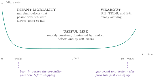
The left wall is infant mortality. Some dies have marginal defects, a via that is thin but not open, an oxide with a weak spot, a bridge that is resistive rather than a hard short. They pass test because at test they still work, then fail within weeks, so the population failure rate starts high and falls as the weak members die off. Burn-in stresses the whole population at elevated voltage and temperature, using the Arrhenius acceleration from 3.5 to compress weeks of field life into a short factory operation.
The trade is real and modern practice has moved. Burn-in consumes life from the good parts too, since the same acceleration that kills weak parts advances BTI and TDDB in healthy ones, so effort has shifted toward better screening, meaning tests that expose marginal parts without stressing everything, such as very-low-voltage testing that makes weak paths fail, quiescent current measurement that exposes resistive shorts, and at-speed transition testing from DFT and Silicon Debug. The right wall is wearout, and all of Part 3 is about pushing it past the product's intended life.
6.4 Field returns, and what a design engineer actually owes
A unit comes back and somebody has to determine whether it is a design bug, a marginal part, a wearout failure, or the customer's problem, since that drives whether a recall is needed. The flow runs from reproducing the failure, to characterizing it against voltage and temperature, which is the shmoo idea from DFT and Silicon Debug, to scan and BIST for localization, to physical failure analysis when the electrical work runs out. Physical analysis is slow, expensive, and destroys the part, so everything cheaper is exhausted first. The design's contribution was made years earlier and is entirely observability, meaning error logging registers recording what happened and where, separate correctable and uncorrectable counters since a rising correctable count is the single most useful field signal there is, and machine check registers that survive the fault. A failure you cannot localize is a failure you cannot fix.
Most of Part 6 belongs to physical design and reliability specialists. Four things are genuinely the RTL and microarchitecture engineer's. Current density awareness on high-activity nets, since anything with high toggle rate and large fanout is an EM candidate and the clock tree is the extreme case, so one enormous buffer driving a huge net is worse than several distributed smaller ones. Not creating hot spots, since a block concentrating all its switching into a small region ages that region faster by Arrhenius and leaks more there. Protecting state according to consequence, which is the triage in 5.5. Providing observability, because nobody can add it after tapeout.
07.Part 8, check yourself
Answer out loud, in full sentences, as if an interviewer asked. If you cannot, reread the section named.
- Reliability is one word for three different questions. State all three and say which tool finds each. (1.1)
- Explain why two transistors from the same mask on the same wafer have different thresholds. Count the dopant atoms in a 20 nm channel and give the fractional spread. (2.1)
- Distinguish systematic from random variation, give two examples of each, and say why dummy fill helps one and not the other. (2.2)
- Why is within-die variation more expensive than die-to-die variation, even though die-to-die variation is usually larger? (2.3)
- A path has ten stages each with a three-sigma spread of ten percent. Compute the margin a blanket derate charges and the margin statistics justifies, and explain why advanced OCV derates shrink with path depth. (2.4)
- Explain NBTI physically, state its time dependence, compute how much of a ten-year drift happens in year one, and say why a static signal ages worse than a toggling one. (3.1)
- A design must guarantee 3.0 GHz for ten years and degrades six percent. What could the fresh silicon run, and what is the aging guardband costing you? (3.1)
- Why does HCI argue for a cold signoff corner when everything else argues for a hot one? (3.2)
- Why does TDDB put a hard ceiling on the top of a DVFS voltage table, and roughly what does 100 mV of extra voltage do to oxide lifetime? (3.3)
- Work out the current limit of a 40 nm by 80 nm wire at 1 MA per square centimetre, compare it against a clock buffer driving 300 fF at 3 GHz, and say what the layout must do about it. (3.4)
- Derive the "rate doubles per ten degrees" rule from the Arrhenius form with eV, then say what going from 60 to 100 degrees does to a ten-year lifetime. (3.5)
- Define FIT. A design has 2000 FIT. Give the single-device MTBF and then the failures per day across a fleet of ten million, and explain why the first number is reassuring and the second is not. (4.2)
- Distinguish SEU, SET, and MBU. Explain why SET-induced errors worsen with frequency, and what layout trick turns an MBU into something SECDED can handle. (4.4)
- What is architectural vulnerability factor, why does raw FIT overstate the problem, and name three structures with near-zero AVF. (4.5)
- A branch predictor is one of the largest arrays on the core and gets no protection, while a dirty L2 line gets SECDED and scrubbing. Justify both from the same principle. (5.5)
08.Part 9, related notes
- SRAM Arrays and ECC for the 6T cell, SECDED, scrubbing, and interleaving, which is where Part 4's soft error rate is actually paid for
- Power Fundamentals and Clock Gating for threshold voltage, the leakage-versus-temperature relationship Part 3 reuses, and the clock tree activity that makes it the worst electromigration case
- DVFS Droop and Thermal for IR drop, di/dt, the power grid, and the thermal loop that Part 3's Arrhenius dependence closes on a timescale of years
- STA Synthesis and Physical Design for OCV and advanced OCV, and for where EM and IR drop sit in signoff
- DFT and Silicon Debug for testing, screening, built-in self-repair, shmoo plots, and the observability infrastructure 6.4 depends on
- Digital Logic and Timing for the delay model, setup and hold, and the capture window that turns an SET into an SEU
- Out of Order Execution for the flush and replay machinery that 5.3 reuses as an error recovery path
- Cache Organization and Prefetching for the dirty-line and clean-line distinction driving the protection triage
- Trends, Constraints, and Quantitative Principles for the vault's treatment of dependability, MTBF, availability, and the yield model
- From Logic to Silicon for the vault's transistor, delay, and scaling background