Advanced-node signoff and the EDA vocabulary interviewers use
September 8, 2026144 min readadvanced
There is a specific and slightly humiliating failure mode in a technical screen, and it is worth naming before doing anything about it.
01.Part 1, what this note is, and why a vocabulary note is worth writing
1.1 The gap, stated precisely
There is a specific and slightly humiliating failure mode in a technical screen, and it is worth naming before doing anything about it.
An interviewer asks how you managed timing across corners. You give a correct, well-reasoned, first-principles answer about process variation, about setup being worst when everything is slow and hold being worst when everything is fast, about the extra margin you carry for within-die variation, and about how the same fix can help one condition and hurt another. Every sentence is true. You have plainly done the work.
And the interviewer writes down "did not mention MMMC."
That is not because the interviewer is shallow. It is because a screen is a sampling process under time pressure. Thirty minutes is not enough to establish that somebody understands a domain, so the interviewer samples for markers that correlate with having lived in it. Vocabulary is the cheapest marker available. Somebody who has run a signoff flow says "we had thirty-two views" without being prompted, because that is the unit the work is organised in and the number is on a dashboard they looked at every day. Somebody who has read about signoff says "we checked several corners," which is the same fact carrying no evidence.
So this note is deliberately not a concepts note. Note 20 is the concepts note and it is good. This is the note that attaches the industry's nouns to the concepts already in your head, adds the arithmetic that makes the nouns concrete, and gives you a defensible way to talk about tools you have used and tools you have not.
1.2 The honesty constraint, which is load-bearing
There is an obvious way to misuse a vocabulary note, and it fails immediately.
Naming a tool invites a follow-up about the tool. If you say "we signed off in PrimeTime" the next question is some variant of "what did your scenario setup look like" or "how did you handle the ECO loop," and if the name was decoration the conversation ends there, badly, and takes your credibility on everything else with it. A candidate who names nothing and reasons well is fine. A candidate who names things and cannot follow through is finished.
So the rule for this whole note, and it is the rule that makes the note safe to use, is: name the class of problem confidently, name the tool only where you used it, and describe function rather than mechanism everywhere else. "That is a power integrity problem, so it is a RedHawk or Voltus question, and it was not mine. The physical design team owned it and gave us back an IR map" is an excellent sentence. It names two tools, claims neither, demonstrates you know what class of problem they solve and who owns it, and closes the follow-up rather than opening one you cannot survive.
Everything below is written to that standard. Where the note describes what a tool does, it describes what class of problem it solves, at the level a vendor's public product page supports. It does not describe tool internals, option names, or version-specific behaviour, because those are exactly the details that are unverifiable from outside and that an interviewer who uses the tool daily will catch instantly.
1.3 How to read it
Parts 2 and 3 are the core: multi-mode multi-corner built from one timing check upward, then the corner and variation vocabulary. Part 4 is the tool landscape, which is a reference part rather than a reasoning part and should be skimmed and then memorised as a table. Part 5 is the signoff checklist as a flow. Part 6 is ECO, which is genuinely new material rather than vocabulary for material you already have. Part 7 is what changes at 7, 5 and 3 nm. Part 8 is floorplan vocabulary. Part 9 is how to talk about the flow ownership you genuinely have.
The last four parts are rehearsal rather than instruction. Part 10 is fifteen interview questions with model answers, the follow-up each invites, and the trap in each. Part 11 is which employers screen on this material and which of your credentials it upgrades. Part 12 is the self-check, and Part 13 is the map back into the rest of the vault.
02.Part 2, multi-mode multi-corner, built from one check upward
2.1 One mode, one corner, one check
Start with the smallest possible thing and put numbers on it, because the whole of MMMC is this object multiplied, and the multiplication is unintuitive only if you never held the single object first.
A flip-flop launches a signal. It travels through some combinational logic. A second flip-flop captures it. Both flops are on the same clock. That is one timing path, and the flop that captures is its endpoint.
Give it numbers. The clock period is ps, so 2 GHz. The launching flop takes ps to put the value on its output after the clock edge. The combinational logic takes ps. The capturing flop needs the data stable ps before its clock edge. Take the clock skew as zero for now.
The data arrives at the capture flop's input at
It is required to be there at
and the slack is the difference,
Positive slack means the check passes. That is one setup check on one endpoint. There is also a hold check on the same endpoint. It asks the opposite question, whether the data arrived so early that it corrupted the previous cycle's capture, and it uses the minimum delays rather than the maximum ones, which makes it a genuinely different arithmetic problem on the same physical path.
Now scale it once. A mid-sized block has on the order of 50,000 to 500,000 sequential endpoints. Take 200,000. So the single object above, done once, is really 200,000 setup checks and 200,000 hold checks, plus the recovery, removal, minimum-pulse-width and clock-gating checks that ride along with them. Call the whole sweep one analysis. It reads the netlist, the library, the parasitics and the constraints, and it produces a number for every endpoint.
One analysis is what most people picture when they say "we ran timing." The entire content of MMMC is that one analysis is not one analysis.
2.2 Add a second mode, and watch the answer change rather than scale
A mode is a functional configuration of the design, and it is defined by its own constraint file. Different clock definitions, different exceptions, different input and output budgets, sometimes a different logical connectivity because muxes are held in different positions.
The temptation is to think a second mode just re-runs the same sums with different constants. Work an example and see that it does not.
Take the same physical path and put the design in scan shift mode. During scan shift every flop is chained into a long shift register. The flop's data input comes from the previous flop's output through the scan multiplexer, not from the functional logic at all. The shift clock is slow, say 100 MHz, so ps.
Redo the setup arithmetic. The combinational path between two adjacent scan flops is now one multiplexer, roughly 30 ps. So
and the slack is ps. Setup in scan shift is not a problem and never will be. If modes were only about numbers, this mode would be pointless.
Now do hold in scan shift, and the picture inverts completely. The hold check does not contain at all. It says the data must not arrive too early:
Put in numbers. ps because the fast corner is quick. The combinational path is one scan mux at its fastest, ps. The capture flop needs ps. And the two flops in a scan chain can be anywhere on the die relative to each other, because the chain is stitched for physical convenience rather than logical locality, so the clock skew between them can be large. Say ps.
That is a 35 ps hold violation, in a mode whose setup check passes with more than a hundred times the margin it needs, 70 ps of arrival against 9,975 ps of requirement. And it is not a corner case. Shift-mode hold is one of the most common late-stage problems in a real block, because the shift path is deliberately the shortest logic in the design and the skew across a long chain is deliberately not managed to functional-mode tightness.
Take the lesson exactly. A mode is not the same analysis with different constants. It is a different question, and its answer can be qualitatively different, passing where the other fails and failing where the other passes. That is why you cannot pick the "worst" mode and run only that one. There is no worst mode.
The modes a real block carries typically include the functional mode at each distinct clock configuration, scan shift, scan capture, at-speed transition test, memory built-in self-test, boundary scan, and any retention or low-power configuration where clocks or resets are held in unusual positions. Seven or eight is ordinary. More than a dozen happens.
One distinction gets fumbled constantly and is worth pinning down now, because it is a cheap thing to get right. Two different operating frequencies of the same logical function are two modes, because the SDC differs, since create_clock names a different period. Two different supply voltages of the same logical function at the same frequency are two corners, because the SDC is identical and only the library characterisation differs. If you take nothing else from this part, take that sentence.
2.3 Add corners, and the check that passed now fails
A corner is a condition the silicon is manufactured and operated in, plus the electrical data that describes it. Concretely it bundles three things. The first is a set of characterised cell libraries at some process, voltage and temperature. The second is a parasitic extraction condition for the wires. The third is the operating voltage and temperature the tool uses for anything it computes rather than looks up.
Take the path from 2.1, which had ps of slack, and move it from the typical corner to the slow one. Typical was TT process, 0.90 V, 25 °C. Slow is SS process, 0.81 V, 125 °C.
Every cell in the path gets slower for the three independent reasons in Part 6.1 of STA Synthesis and Physical Design. Suppose the combined effect is a factor of roughly 1.5 on cell delay, which is the right order for a ten percent voltage drop plus a slow process plus a hot die, though the exact multiplier is entirely process-specific and you should never quote one as though it were universal. Then
The identical netlist, in the identical mode, on the identical path, has gone from comfortably passing to failing by nearly a third of the clock period. Nothing about the design changed. A corner is not a safety factor applied to an answer. It is a different circuit, and it produces a different answer.
Now do the fast corner, which is FF process, 0.99 V, and a low temperature, and check hold on a short path. Take a short path with ps, ps, ps, and a positive skew of 40 ps from the launch flop to the capture flop:
A 15 ps hold violation, at the corner where the setup check passes most easily. So setup and hold do not merely prefer different corners. They are checked at opposite ends of the same axis, and a design that has been verified at one end has been verified for exactly one of the two.
That gives the corner axes. Process takes at least SS, TT and FF and often the mixed SF and FS. Voltage takes every operating point in the DVFS table plus the tolerance band around each, per DVFS Droop and Thermal. Temperature takes both extremes, and because of the temperature inversion effect in Part 6.1 of note 20 you genuinely cannot drop the cold one. Interconnect takes its own set, which Part 3 of this note develops, because the metal stack varies independently of the transistors.
2.4 The scenario count, with real arithmetic
Now multiply, because the number is the point and most people have never worked it.
A scenario is one mode paired with one corner. The Cadence-family word for the same object is view, and the two are used interchangeably in conversation. A scenario is the unit of work, and one scenario is one full analysis over every endpoint.
Take a realistic list for a modern block.
| Axis | Values | Count |
|---|---|---|
| Mode | functional nominal, functional turbo, functional low-power, scan shift, scan capture, at-speed transition, MBIST | 7 |
| Process | SS, TT, FF | 3 |
| Voltage | 0.65 V, 0.75 V, 0.90 V | 3 |
| Temperature | −40 °C, 25 °C, 125 °C | 3 |
| Interconnect | Cworst, Cbest, RCworst, RCbest, typical | 5 |
The naive cross product is
Nine hundred and forty-five full timing analyses, each over 200,000 endpoints, each requiring the netlist, the libraries for that corner, and a full set of extracted parasitics for that interconnect condition.
Price it in resources, because that is what makes it real rather than a number on a slide. Say one scenario takes two hours of wall time and 40 GB of memory on one compute node. Then a full pass is
Run it 100-way distributed and a single full pass is a little under nineteen hours. During timing closure you want several passes a day, because each ECO iteration must be re-checked, so nineteen hours per pass is not a slow flow, it is a broken one. And 945 scenarios at 40 GB is 37.8 TB of resident memory if you truly ran them all at once, which no farm allocates to one block.
There is a second cost that is worse than the compute, and it is the one that decides how a project actually feels. Every fix must be re-checked against every scenario. Add a buffer to fix setup at the slow corner and you have added delay that exists at the fast corner too, where it may create a hold violation. Downsize a cell to fix that hold violation and you may reopen the setup problem. With one scenario that loop converges in an afternoon. With 945 it does not converge at all, because the number of coupled constraints exceeds anybody's ability to reason about which fix is safe.
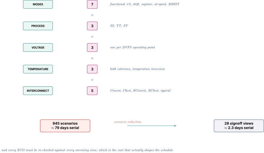
2.5 Scenario reduction is a real engineering activity
Because 945 is impossible, somebody reduces it. That somebody is a senior person, the reduction is documented, it is signed, and it is revisited when anything about the design changes. Saying this out loud is a strong marker, because it is the part of MMMC that only exists if you have been in the room.
Four reduction arguments, in decreasing order of how safe they are.
Impossible combinations are free to delete. The cross product includes conditions the silicon will never be in. MBIST does not run at the turbo voltage because the turbo point is a boost condition entered under thermal control, not a test condition. Scan shift does not run at the lowest voltage because shift is a manufacturing-floor operation at a nominal setting. The low-power functional mode does not exist at 0.90 V because the whole point of that mode is that the rail dropped. Every such deletion removes a whole slab of the product, and none of them costs anything, because you are not declining to analyse a condition, you are observing that the condition does not exist.
Dominance removes scenarios that cannot be the binding one. If scenario A is slower than scenario B on every path in some path group, then B cannot report a setup violation that A does not also report, and B can be dropped for setup. This is the argument people reach for first and it is the one to be most careful with, because dominance is easy to assert and hard to prove. Cell delay does not scale uniformly across a library. A cell whose critical transition is PMOS-driven and one whose critical transition is NMOS-driven move differently between corners, so "slower everywhere" is often false in detail even when it is true on average. The defensible version of the argument is per path group and per check type, not global.
Setup and hold split the corner list. Setup is dominated by the slow end of the process-voltage-temperature space and hold by the fast end, so a scenario can be enabled for setup only, or hold only, rather than both. That roughly halves the analysis work for most of the list. Temperature inversion complicates it, since at low supply the cold corner can be the slow one. That is exactly why the low-voltage entries need both temperature extremes and the high-voltage ones may not.
Interconnect corners are chosen against what the block actually contains. Part 3.3 works out why a short net and a long net are worst at different interconnect conditions. A block whose longest net is 200 µm does not need the same interconnect list as one containing a millimetre-long bus, and pruning on that basis is a genuinely local, genuinely justified argument.
Then there is a structural move that is not a reduction but has the same effect on schedule. Run a small "driver" list during implementation and the full pruned list at signoff. The implementation tool optimises against perhaps four to eight views chosen because they bind, typically the slow setup view, the fast hold view, one or two mid-voltage views, and a test-mode view. The signoff tool then runs the full pruned list, perhaps 20 to 40 views, less often. That two-tier structure is close to universal and knowing it exists is the difference between having read about MMMC and having lived in it.
Finish honestly, because the honest version is the impressive one. Scenario reduction is a risk decision, not an optimisation. Every scenario you delete is a condition the chip may see and you have chosen not to analyse. If the argument was wrong, the failure appears in silicon, at one temperature or one voltage, on parts from one wafer lot, months later, and is close to untraceable. That is why the list has an owner, why the justification is written down rather than remembered, and why it gets re-audited whenever the DVFS table, the library, the test methodology or the floorplan changes.
2.6 The vocabulary itself, and how much of it to use
Now attach the words, with the hedging the subject requires.
MMMC means multi-mode multi-corner and it is spoken as a single word, "em-em-em-cee." It is used both for the analysis style and for the configuration that describes it, as in "the MMMC setup" and "the MMMC file."
In the Cadence family the configuration is built from named objects that stack: a library set groups the .lib timing libraries for one condition, an RC corner names the extraction data, a delay corner pairs a library set with an RC corner, a constraint mode names an SDC file, and an analysis view pairs a delay corner with a constraint mode. Views are then declared active for setup and for hold. The whole thing is saved as a view definition file of Tcl commands. That vocabulary of library set, RC corner, delay corner, constraint mode and analysis view is documented publicly and is exactly what you would hear in an Innovus or Tempus shop.
In the Synopsys family the unit is called a scenario, and PrimeTime's mechanism for running many of them concurrently across a compute farm is publicly described as distributed multi-scenario analysis, or DMSA. The important idea, and the one worth stating, is that the scenarios are analysed concurrently in one session rather than as independent jobs, so that a fix can be evaluated against all of them at once instead of serially.
Do not go past that. Do not quote command syntax, option names, or what a particular release does, because the details differ by version and by site and an interviewer who uses the tool will know. Describe the objects and the structure, name the tool, and stop. If you are asked how you set yours up, describe your view list. Say how many there were, what they covered, and why those and not others. That is the answer that demonstrates ownership, and it is true.
03.Part 3, PVT corners, the interconnect axis, and the variation vocabulary
3.1 SS, TT, FF, and the two corners people forget
The process corner names are two letters, and the letters are NMOS first, PMOS second. So SS is slow-NMOS slow-PMOS, FF is fast-fast, TT is typical-typical. Those three cover the case where the whole wafer came out uniformly fast or uniformly slow, which is the dominant mode of process variation and the reason they are the three everybody names.
The two that get forgotten are SF, slow-NMOS fast-PMOS, and FS, fast-NMOS slow-PMOS. They exist because the N and P devices are formed by partly independent process steps, with different implants, different work-function metals and different stressors, so they can skew in opposite directions. They matter for a specific and namable class of circuit: anything where a rising edge races a falling edge.
Work out why that is a real category rather than a curiosity. In a CMOS inverter the output rises through the PMOS network and falls through the NMOS network, so a rising transition's delay is set by the P devices and a falling transition's delay by the N devices. At SS and FF the two move together, since both device types slow down or both speed up, so a delay measured from a rising edge and a delay measured from a falling edge stay in roughly the same proportion. At SF and FS they move in opposite directions, so that proportion changes. Any circuit whose correctness depends on the proportion rather than on either delay alone is therefore exposed at SF and FS and nowhere else.
Now consider a pulse generator built as an AND of a signal with its own delayed inverse. Its pulse width is set by a path ending on one edge polarity racing a path ending on the other, so it is exactly such a circuit. At SF and FS the two contributions skew apart and the pulse width moves off its nominal value. Which of SF and FS widens it and which narrows it depends on the specific topology. It turns on the parity of the delay chain and on which edge terminates the pulse, so derive it for the circuit in front of you rather than memorising a direction. The point that generalises is that one of the two mixed corners is the bad one, and neither SS, TT nor FF will show you which. A pulse-width-dependent circuit can be perfectly correct at SS, TT and FF and broken at a mixed corner, and that category includes the pulsed latch, the self-timed SRAM word line, the duty-cycle-sensitive clock structure and the level shifter.
The same applies to any structure whose correctness depends on the ratio of two delays rather than their sum: a clock-gating check where the enable path and the clock path have opposite final polarities, a matched-delay dummy path, a differential sense amplifier, a race between a set and a reset. If your block contains none of those, SF and FS are usually pruned. If it contains one, they are not, and knowing which category your block is in is exactly the kind of local judgment that scenario reduction is made of.
3.2 Why the wires get their own axis
Here is the fact that makes the interconnect corners necessary, and it is a one-sentence argument most candidates have never assembled.
The transistors and the wires are made in different process steps, so their variations are independent. The front-end-of-line steps that set channel length and threshold voltage happen first. The back-end-of-line steps that deposit, pattern, polish and fill a dozen or more metal layers happen afterwards, on different equipment, with different control loops. A wafer that came out slow for the transistors has no particular tendency to come out thick or thin for metal 4.
If the two were correlated you could fold interconnect into the PVT corner and be done. Because they are not, the corner list needs a separate axis, and that axis has more than two positions for a reason that takes arithmetic.
3.3 Why there are four or five interconnect corners and not two
The instinct is that there should be exactly two, a fat-wire condition and a thin-wire condition. Work an example and the instinct breaks.
A wire has resistance and capacitance . Metal that comes out thicker and wider has lower resistance, because the cross-section is larger, and higher capacitance, because more surface faces the neighbouring wires. Metal that comes out thinner and narrower has the reverse. So and move in opposite directions, and which combination is worst depends on whether the net you are looking at is dominated by its resistance or by its capacitance.
Take a driver whose output resistance is , a plausible figure for a small standard cell, and give it two different nets. Use the lumped estimate , which is the standard first-order form. The driver sees the whole wire capacitance, and the wire's own distributed contributes roughly half the product. Treat every number here as illustrative rather than as data from any real stack.
A short local net. fF, .
The driver term is forty times the wire term, so this net is capacitance-dominated. Put it at a condition where capacitance is maximum and resistance minimum, say 15 percent more and 10 percent less :
At the opposite condition, 15 percent less at 4.25 fF and 10 percent more at 110 Ω, it is ps. So for this net the maximum-capacitance condition is the worst one by a clear margin, and resistance barely participates.
A long global net. fF, .
Now the two terms are equal, so resistance matters as much as capacitance. At the maximum-capacitance condition, which also lowers resistance:
And at a condition chosen to maximise the product instead, say 10 percent more capacitance with 25 percent more resistance, which is physically reachable because the dielectric thickness varies independently of the metal width:
396 ps beats 350 ps. The condition that was worst for the short net is not worst for the long one. A corner list containing only maximum-capacitance and minimum-capacitance would sign the long net off at 350 ps and ship a part where it takes 396.
That is the whole justification, and it is why foundries supply a set rather than a pair. The names are broadly standardised across the industry and broadly, but not exactly, consistent between foundries and extraction tools, so use them with a light hedge.
| Name | Roughly what it represents | Where it binds |
|---|---|---|
| Cworst, also Cmax | maximum capacitance, resistance low | short, capacitance-dominated nets, setup |
| Cbest, also Cmin | minimum capacitance, resistance high | short nets, hold |
| RCworst | maximum product | long, resistance-dominated nets, setup |
| RCbest | minimum product | long nets, hold |
| Typical | nominal everything | correlation and reference |
Advanced-node kits often add variants that separate the coupling capacitance between adjacent wires from the total capacitance to ground, because crosstalk analysis cares about the coupling term specifically while ordinary delay cares about the total. Those appear with suffixes indicating whether coupling is at its high or low value. The exact set, the exact names and the exact definitions are foundry-specific and are supplied with the process design kit, so do not quote a particular foundry's list from memory in an interview. Describe the structure and say the kit defines the list.
One more piece of vocabulary lives here and is worth knowing because you will see the filename. The extracted parasitics are handed from the extraction tool to the timer in SPEF, the Standard Parasitic Exchange Format, one file per interconnect corner. That is why adding an interconnect corner is expensive in a way that adding a voltage is not. A voltage is a different set of .lib files that already exist. An interconnect corner is a full re-extraction producing another multi-hundred-megabyte parasitic database.
3.4 On-chip variation, and the vocabulary for handling it
The physics and the arithmetic are in Part 6.4 of STA Synthesis and Physical Design and this section deliberately does not repeat them. Read that section for the averaging argument and the common-path arithmetic. Read this one for what the things are called.
A corner captures die-to-die variation, meaning that this whole die came out slow. Nothing in a corner captures within-die variation, the fact that two nominally identical inverters a hundred microns apart on the same die differ. So an extra mechanism is layered on top, and it has four generations of vocabulary.
OCV, on-chip variation, is the umbrella term. The crude implementation is derating. Multiply every cell on the launch path by something above one and every cell on the capture path by something below one, so the analysis assumes the worst combination. Tool-side that is set_timing_derate, and a flow using one number for the whole design is said to use flat or blanket derate.
CPPR, common path pessimism removal, credits back the impossible part of that assumption, namely that the buffers physically shared between the launch and capture clock paths were simultaneously slow and fast. The same feature is called CRPR, clock reconvergence pessimism removal, in some tools. Both names refer to the same correction and both are in current use, so recognising both is worth more than picking one.
AOCV, advanced on-chip variation, replaces the single derate factor with a table indexed by the number of stages in the path and by the physical distance the path spans. Deep paths are derated less because random variation averages out along them. Physically spread-out paths are derated more because they see more systematic across-die variation.
POCV, parametric on-chip variation, goes statistical. Each cell carries a mean delay and a standard deviation, the tool combines them along the path as random variables rather than as worst cases, and slack is reported at a chosen sigma, three sigma being the common signoff point. The library data that makes this possible is carried in LVF, Liberty Variation Format, an extension to the .lib format holding per-cell, per-arc variation moments. At advanced nodes LVF data is not optional in the kit, because the underlying delay distributions become skewed enough that a mean and a sigma are no longer sufficient and the format carries higher moments too. The name to know is LVF, and the sentence to have ready is that POCV is only as good as the LVF data behind it, so a flow running POCV against a library without proper LVF characterisation has bought precision rather than accuracy.
Cadence's statistical variant is sometimes called SOCV. Treat the two families as solving the same problem under different marketing, because that is what they are, and do not claim to know how their internals differ.
The one-sentence version to say out loud: a corner handles die-to-die variation, OCV handles within-die variation, CPPR removes the self-contradiction in a naive OCV model, and AOCV and POCV replace a single number with a depth-aware table and a statistical distribution respectively. That covers the whole subject and is defensible in every clause.
3.5 The words you will actually hear in a review
Short reference list, because these appear in conversation with no explanation and not recognising them is expensive.
WNS, worst negative slack, the single worst endpoint. TNS, total negative slack, the sum over all failing endpoints. Together they give the shape of the problem, per Part 5.5 of note 20: a large WNS with a small TNS is one bad path, a small WNS with a huge TNS is a systemic budget problem, and they call for opposite responses. NVP and FEP, number of violating paths and failing endpoints, which are counts rather than magnitudes.
Path group, a named partition of the endpoints, typically one per clock plus input-to-register, register-to-output and input-to-output, reported separately so that a hundred failing input paths do not hide two failing internal ones.
View or scenario as established in 2.6. Signoff used as a verb, meaning the specific run with extracted parasitics, signoff-grade delay calculation and the agreed OCV settings, as distinct from the estimates the implementation tool works with. Correlation, the agreement between two tools or two stages that ought to report the same thing, as in "our implementation-to-signoff correlation is within 10 ps," which is a health metric rather than a result. Waiver, a documented decision to ship a violation. Clean, zero violations across the signoff list. Turn or iteration, one full loop of fix, re-extract, re-time. Freeze, the date after which a given class of change is no longer accepted.
04.Part 4, the signoff tool landscape, by name
4.1 How to hold this material
This part is a reference rather than an argument. Read it once, then memorise the table in 4.8 and forget the prose.
The framing that keeps it safe is that the industry has, for each class of problem, roughly two credible commercial answers, and knowing the pair is the signal. Naming one tool proves you saw a logo. Naming the pair and saying what class of problem they solve proves you know the shape of the industry, which is what the question is actually probing. "Timing signoff is PrimeTime or Tempus, physical verification is Calibre and its two competitors, power integrity is RedHawk or Voltus" is three sentences that cover most of what a screen wants.
Two ownership facts to keep current because they change the branding you will see. Synopsys completed its acquisition of Ansys on 17 July 2025, so RedHawk-SC now appears under Synopsys branding while remaining the same tool with the same foundry certifications. As a regulatory condition of that deal, two products went the other way: Ansys' PowerArtist RTL power product and Synopsys' Optical Solutions Group were both divested to Keysight, which closed on 17 October 2025. That matters here for one specific reason. PowerArtist is an RTL power tool, so it sits in the same class as Cadence Joules in Part 4.5, and it is no longer a Synopsys or Ansys product. Naming it under either is the kind of stale-by-one-year mistake that is easy to avoid and awkward to make. Siemens owns what used to be Mentor Graphics, so Calibre is a Siemens product and has been for years, and calling it "Mentor Calibre" dates you slightly without being wrong.
4.2 Synthesis and implementation
Synopsys Design Compiler is the long-standing logic synthesis tool. It reads RTL and an SDC constraint file, and produces a gate-level netlist mapped to a standard cell library. The current generation is branded Design Compiler NXT. This is the tool most front-end engineers have actually touched, because synthesis is where an RTL designer's own quality of results is measured.
Synopsys Fusion Compiler is an RTL-to-GDSII implementation system. Rather than synthesis and place-and-route being separate tools exchanging netlists, it runs both on a single shared data model so that synthesis can already reason about placement and routing. Synopsys publicly describes it as fusing high-capacity synthesis with the IC Compiler II place-and-route engine. The concept to attach the name to is physical synthesis, meaning synthesis that knows where things are, which note 20 covers in Part 8.7 without naming a product.
Synopsys IC Compiler II is the place-and-route tool, and is the engine inside Fusion Compiler.
Cadence Genus is the competing synthesis tool. Cadence Innovus is the competing implementation system, covering floorplan, placement, clock tree synthesis, routing and optimisation. A shop is usually predominantly one family or the other, because the constraint files, scripts, tribal knowledge and the MMMC configuration format are all family-specific, but mixed flows exist and are common at the boundaries.
Siemens Aprisa is a third place-and-route option with a smaller share. Knowing it exists is enough.
4.3 Timing signoff
Synopsys PrimeTime is the incumbent signoff static timing analysis tool and is what "signoff STA" means at most companies. PrimeTime SI is the crosstalk-aware variant, adding the delta-delay and noise analysis of Part 5.3 below. DMSA, distributed multi-scenario analysis, is its mechanism for running many scenarios concurrently across a farm.
Cadence Tempus is the competing signoff timer and is the natural pairing in an Innovus flow.
The discipline to state, which is in Part 9.1 of note 20 and is worth naming here as a tool decision rather than a philosophy: the signoff timer should be a different engine from the one inside the implementation tool. An implementation tool's internal timer is tuned for speed because it evaluates millions of candidate changes. If it is optimistic in some corner of its delay model, and it also signs the result off, the optimism never surfaces. Using an independent engine means a systematic error in one has to coincide with the same error in the other to escape. That is why "our implementation-to-signoff correlation" is a metric people track.
4.4 Parasitic extraction
Synopsys StarRC and Cadence Quantus are the two parasitic extraction tools. They read the routed layout plus the foundry's extraction technology file, and emit the resistances and capacitances of every net as a SPEF file per interconnect corner. That SPEF is what turns an estimate-based timing run into a signoff-grade one.
The reason to know this exists as a separate tool rather than a feature is that extraction is where the foundry's proprietary characterisation of its own metal stack enters the flow. The tech file is a deliverable of the process design kit, it is qualified by the foundry, and it is the reason two extraction tools can disagree slightly on the same layout and both be defensible.
4.5 Power and power integrity
Two distinct classes get confused and separating them cleanly is itself a marker.
Power analysis answers "how many watts." It reads a netlist, a library with power data, and a switching activity file from simulation in SAIF, FSDB or VCD form, and reports average and time-varying power per instance, per module and per clock. Synopsys PrimePower is the signoff tool here. Cadence Joules works earlier, at RTL, trading accuracy for the ability to answer the question before a netlist exists. This class of problem is the subject of Power Analysis Flow and Methodology, and it is the tool class that produced the per-instance clock-power report behind the clock-gating work in Part 4.1 of Power Fundamentals and Clock Gating.
Power integrity answers a completely different question, "does the voltage actually arrive." It analyses the power delivery network itself, meaning the grid of wide metal straps, the vias between layers and the bumps feeding them, and it reports three things. Static IR drop is the steady voltage lost across grid resistance. Dynamic voltage drop is the transient collapse when many cells switch at once. Electromigration is the slow physical destruction of metal carrying too much current density, per Part 9.3 of note 20. Ansys RedHawk-SC, now under Synopsys, and Cadence Voltus are the two tools. RedHawk-SC is the more common choice for final signoff, and the fact to attach to it is that foundries certify it against their own processes at the leading nodes. Ansys has publicly announced certifications spanning TSMC's 3 nm generation and Samsung's 3 nm, 2 nm and backside-power variants, which by now covers both finFET and gate-all-around processes. Say "foundry-certified at the leading nodes" rather than naming a specific node, because the certification list grows every year and quoting last year's is worse than quoting none. Voltus is the natural pairing inside a Cadence implementation flow.
The sentence that separates them: power analysis tells you how much energy the design consumes, power integrity tells you whether the delivery network can supply it without the voltage sagging below what the timing analysis assumed. They are usually owned by different people, and a front-end engineer normally consumes the second one's output, an IR map fed back into timing, rather than running it.
4.6 Physical verification
Siemens Calibre is the dominant physical verification platform and has been the de-facto signoff standard at most foundries for a long time. Its components carry the nm prefix: Calibre nmDRC for design rule checking, Calibre nmLVS for layout-versus-schematic. The -Recon variants run reduced-scope early checks on incomplete designs so that a block can be checked before it is finished. The reason Calibre's position is so strong is not primarily technical. The rule decks, the machine-readable encodings of a process's thousands of design rules, are written and qualified by the foundry in Calibre's language, so a Calibre-clean result is what the foundry will accept.
Synopsys IC Validator and Cadence Pegasus are the two competitors, and both are used, particularly where a shop wants physical verification inside its implementation tool's own environment for faster iteration.
4.7 Equivalence and the front-end static checks
Synopsys Formality and Cadence Conformal are the logic equivalence checking tools, proving that a gate netlist implements the same function as the RTL, formally and without simulation. Part 9.4 of note 20 covers what breaks LEC and why each break has a flow answer.
Lint, clock-domain-crossing and reset-domain-crossing checking are the front-end static checks. Synopsys SpyGlass is the name most often heard for lint and CDC. Siemens and Cadence both offer equivalents, and Cadence's formal property tool Jasper is the name to know on the formal side, which is directly relevant given the formal work on your record. Do not attempt to be precise about product-line boundaries in these families, because they have been reorganised repeatedly. Name the tool you used and describe the check.
4.8 The table
| Problem class | Synopsys | Cadence | Other |
|---|---|---|---|
| Logic synthesis | Design Compiler / DC NXT | Genus | none |
| RTL-to-GDSII implementation | Fusion Compiler | Innovus | Siemens Aprisa |
| Place and route | IC Compiler II | Innovus | Siemens Aprisa |
| Signoff STA | PrimeTime, PrimeTime SI | Tempus | none |
| Parasitic extraction | StarRC | Quantus | none |
| Signoff power | PrimePower | Joules (RTL) | none |
| Power integrity, EM/IR | RedHawk-SC (Ansys, now Synopsys) | Voltus | none |
| Physical verification | IC Validator | Pegasus | Siemens Calibre |
| Logic equivalence | Formality | Conformal | none |
| Lint and CDC | SpyGlass | Jasper lint and CDC apps | Siemens Questa |
| Formal property checking | VC Formal | Jasper | none |
The one-line summary to carry out of this part: Synopsys and Cadence each field a complete flow, Siemens owns physical verification through Calibre and holds a smaller position elsewhere, and power integrity is the one place where a specialist tool, RedHawk, held the signoff position across both flows for years.
05.Part 5, the signoff checklist as a flow
5.1 What tapeout actually is, and therefore what is being gated
Tapeout is the moment the design database is released to the mask shop. The name is a fossil from when the data left on magnetic tape. After it, the geometry is turned into physical photomasks, and photomasks are expensive, slow to make, and not editable.
That is the entire reason the checklist exists and the entire reason it is so heavy. Every other stage of the flow is reversible in hours. This one is reversible in months and millions of dollars, and Part 6.3 puts numbers on that. So before the data leaves, a fixed list of checks must each be either clean or explicitly waived by a named owner, and the list is tracked on a dashboard that the whole project stares at daily for the last several weeks.
The useful mental model is not a pipeline. It is a set of independent gates that must all be open simultaneously, on the same version of the database, at the same time. And they are coupled, so opening one can close another. That coupling is the subject of 5.7 and it is the thing that makes the last two weeks of a project what they are.
5.2 Timing, and the checks that ride along with it
Timing signoff means every view in the pruned list from Part 2.5, clean or waived, on extracted parasitics, with the agreed OCV settings, in the signoff timer rather than the implementation tool.
Within a view, five distinct checks run and naming all five is a marker, because most people name two.
Setup, the data arrived before the capture edge minus the setup time. Hold, the data did not arrive so early that it corrupted the previous capture. Those two are the ones everybody names.
Recovery and removal are the same two checks applied to an asynchronous reset relative to the clock edge that releases it. Recovery is the reset's setup analogue. De-assert too close to the edge and the flop may go metastable on release. Removal is its hold analogue. This is the timing-side expression of the reset-release problem in Clocking Reset and Domain Crossing, and the fact that it appears as an ordinary timing check with an ordinary slack number is worth knowing.
Minimum pulse width checks that every clock pulse reaching every flop is wide enough for the flop to be characterised against. This is where clock gating comes back to bite, because an integrated clock gating cell that produces a slightly truncated pulse fails here, and it is why the ICG structure in Part 3.2 of Power Fundamentals and Clock Gating has to guarantee a full-width copy or nothing.
Clock-gating checks verify the relationship between a gating enable and the clock it gates. Note 20 flags in Part 5.2 that these form their own path group, and that the enable path sees negative skew because the gater sits upstream in the clock tree from the flop that launches the enable. That is the exact structure behind the "why did synthesis refuse to gate this register" answer in Part 4.2 of note 17, expressed as a timing check.
There is also maximum transition, maximum capacitance and maximum fanout, the electrical rules of Part 3.4 of note 20, which are not timing checks at all but are reported alongside and gate the same way. A design can be timing-clean and still fail signoff on a single net with a 500 ps transition time, because that net's slew was never characterised and its delay number is therefore an extrapolation nobody trusts.
5.3 Noise and crosstalk, which is a separate signoff and not a footnote
Ordinary static timing analysis treats each net in isolation. That assumption stops being safe once wires are tall, thin and close together, because a wire's capacitance to its neighbours becomes comparable to its capacitance to ground. Once that is true, what the neighbour is doing changes what this net does.
The vocabulary is aggressor and victim. Work the mechanism concretely.
Crosstalk delta delay. A victim net is transitioning low-to-high. Its neighbour, the aggressor, transitions at the same moment. If the aggressor goes the same direction, it pulls the victim along through the coupling capacitance and the victim gets there early. If it goes the opposite direction, it fights the victim and the victim arrives late. So the same physical net has two different delays depending on what happened next to it, and the difference, the delta delay, can be a large fraction of the net's nominal delay when the coupling capacitance is a large fraction of total capacitance.
That creates a genuinely new analysis problem rather than a bigger version of the old one, because the timer now has to reason about whether the aggressor could plausibly switch in the window when the victim is switching. If the two are on unrelated clocks, assume the worst. If they are on the same clock and their timing windows provably do not overlap, the coupling cannot hurt. So crosstalk analysis is iterative: compute timing windows, use them to decide which aggressors are credible, recompute delays, which moves the windows, and repeat until it settles. That is why it is a separate mode of the tool, PrimeTime SI, rather than always-on.
The direction that surprises people is worth volunteering: crosstalk can help as well as hurt, and both are dangerous. A same-direction aggressor speeds the victim up, which is bad for hold. So crosstalk creates setup risk from opposite-direction coupling and hold risk from same-direction coupling, and both must be analysed.
Crosstalk noise, or glitch. Now the victim is not switching. It is being held at a rail by its driver. The aggressor switches. Charge couples across and lifts the victim off its rail by some amount for some duration. Three outcomes. If the bump is small and the victim's receiver has margin, nothing happens. If the bump exceeds the receiver's switching threshold and lasts long enough, a glitch propagates into the logic, and if it reaches a flop's data pin during the capture window it is captured as real data. And if the victim is a node that has no driver holding it, the disturbance simply stays there, because nothing restores it. The classic case is a dynamic node, but a floating node during a power-gated state behaves the same way.
The fixes are structural rather than clever: increase the spacing between the two wires, insert a shield wire tied to a rail between them, upsize the victim's driver so it holds its rail harder, downsize or slow the aggressor, or reroute one of them onto a different layer. Note the tension with everything else. Spacing and shielding consume routing resource, which raises congestion, which is Part 8.
Clock nets are the special case. A clock net is the highest-activity wire in the design, so it is the strongest aggressor in its neighbourhood, and it is also the net where a delta delay translates directly into skew, which moves every setup and hold check downstream of it. Which is why clock routing gets shielding and extra spacing as a matter of course rather than as a fix.
5.4 EM and IR, which are the same analysis run twice
The physics is in Part 9.3 of note 20, which covers Black's equation, the current density in a clock buffer, and the voltage lost across grid resistance. What matters here is the flow shape and the vocabulary.
The tool builds a model of the power delivery network: every strap on every metal layer, every via between them, and the bumps that feed the whole thing from the package. Then it drives that model with a current profile derived from a power analysis run, and reports three things.
Static IR drop is the steady-state voltage lost between the bump and each cell under an average current. It is checked as a percentage of nominal supply, with a target commonly in the low single digits.
Dynamic voltage drop, usually abbreviated DvD, is the transient version. Many cells switching in the same nanosecond draw a current spike, and the grid's inductance and finite decoupling capacitance let the local rail collapse briefly. This is the analysis that catches a coarse clock gater or a power gate waking a whole block at once, which is exactly the inrush mechanism in Part 6.3 of Power Fundamentals and Clock Gating and the droop mechanism in DVFS Droop and Thermal. The output is a map, in space and time, of where and when the rail sagged worst.
Electromigration is checked on two different populations with two different criteria. Power and ground rails carry unidirectional average current and are limited by the average. Signal nets carry bidirectional current that averages to nearly zero, so they are limited instead by the RMS current and the self-heating it causes, which raises the local temperature, which accelerates the very migration process being checked. At advanced nodes signal EM stopped being a formality precisely because wires got thin enough that a hard-driven high-activity net can exceed its limit.
The coupling back to timing is the part to name. An IR map is a delay map. A region at 3 percent below nominal supply runs roughly 4 to 6 percent slower, so a good flow feeds the voltage map back into the timer as a per-instance voltage rather than assuming nominal everywhere. A flow that does not do that has signed off timing at a voltage the silicon does not see in that region.
5.5 Physical verification, and what each check actually proves
Four checks, and the discipline is to be able to say what each one proves that the others do not.
DRC proves the drawn geometry is manufacturable: minimum widths, minimum spacings, via enclosure, density windows, and at advanced nodes several thousand more rules including the multi-patterning colouring constraints of Part 7.4. A DRC violation means either the mask cannot be made or the feature will not print reliably. It says nothing about whether the design is correct.
LVS proves the geometry implements the intended netlist. It extracts devices and connectivity from the polygons and compares them, device by device and net by net, to the schematic netlist. It catches the case where the layout is beautiful, fully DRC-clean, and connects the wrong things. It says nothing about whether the intended netlist is manufacturable.
Antenna checks prove that no transistor gate was exposed to a plasma-charged metal area large enough to damage its oxide during manufacture. Note 20 explains the mechanism in Part 9.2. The check is a ratio of accumulated metal area to gate area, per layer, at each stage of the build, and it is a check about the manufacturing sequence rather than the finished object. That is why it cannot be inferred from the final geometry alone and needs its own rule deck.
Density and fill proves that every window of the die has metal coverage inside a specified band. Too sparse and chemical-mechanical polishing dishes the surface. Too dense and it does not clear. The fix is automatic insertion of fill shapes, floating or grounded dummy metal, which is a real problem for timing because fill adds capacitance to nearby signal nets. So fill must be inserted before the final extraction, not after, and a flow that extracts before filling has under-counted every capacitance in the design.
ERC, electrical rule checking, is the fifth one people forget: floating gates, missing well and substrate taps, unconnected inputs, and power-domain violations where a cell on one supply drives a net on another without a level shifter.
5.6 The rest of the gate list
Logic equivalence between RTL and netlist, per Part 9.4 of note 20. DFT coverage from ATPG plus scan chain integrity, per DFT and Silicon Debug. Power intent static checks plus power-aware simulation, per Part 8 of Power Fundamentals and Clock Gating. Gate-level simulation, which is the check that catches what RTL simulation's optimistic X semantics hide. Reliability and aging margin, per Reliability Aging and Variation. And the assorted hierarchical checks, which confirm that block-level abstractions used at the top match the blocks they abstract, that the top-level assembly's pin assignments match the blocks' actual pins, and that every block signed off against the same version of every library.
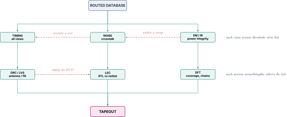
5.7 The convergence problem, and why the last two weeks are the way they are
Now the part that explains the atmosphere of a tapeout, and it follows entirely from the coupling.
Suppose EM signoff reports a strap on metal 6 carrying too much current. The fix is to widen it. Widening it displaces the signal routes that were there, so the router moves them, which changes their length and their neighbours, which changes both their delay and their coupling capacitance. So timing must be re-extracted and re-run, across every view. And crosstalk must be re-run, because the nets have new neighbours. And DRC must be re-run on the changed region. And if timing now fails somewhere, an ECO is required, which adds cells, which changes the current profile, which reopens EM.
That loop has no guarantee of terminating. What makes it terminate in practice is a discipline of decreasing disturbance. Each successive iteration is required to touch less than the last one. Early iterations may re-place and re-route freely. Later ones may only add buffers in existing gaps. The final ones may only resize cells in place, because a resize that fits in the same footprint changes nothing physical except that instance. And past a certain date, nothing is accepted that is not a one-instance change with a written justification.
That is why the schedule is expressed as a series of freezes rather than a single deadline: RTL freeze, then netlist freeze, then a freeze on anything that moves a cell, then a freeze on anything that changes routing, then tapeout. Each freeze closes one feedback arrow in the diagram above so the remaining loop is small enough to converge.
The sentence worth having ready, because it demonstrates you have been in the room: the hard part of signoff is not any individual check, it is finding one version of the database on which all of them pass simultaneously, because fixing any one of them perturbs the others.
06.Part 6, ECO flows
6.1 What an ECO is, and why the concept has to exist
ECO stands for engineering change order, and in this context it means a targeted, incremental change applied to a design that is already implemented, instead of re-running the flow from the source.
Start with why you would not simply re-run. Suppose two weeks before tapeout somebody finds a bug in a control state machine. The obvious response is to fix the RTL and re-synthesise. Do that and the synthesis tool, which is a heuristic optimiser making millions of choices, will produce a completely different netlist, with different cell choices, different structuring, and different instance names throughout. Place and route will then produce a completely different layout. And every result you have accumulated over the past four months, every closed timing path, every EM fix, every DRC waiver, every characterised block abstraction, every gate-level simulation run, applies to a design that no longer exists.
So the economics invert. Late in a project, preserving what already passed is worth more than getting an optimal result, and an ECO is the mechanism for buying that preservation. The ECO changes the netlist minimally and changes the layout in a bounded region, so everything outside that region is provably untouched and does not need re-verifying from scratch.
Two orthogonal axes classify every ECO, and keeping them orthogonal is the thing to get right, because they are routinely conflated.
The first axis is what changed: functional or timing. The second axis is when it changed relative to the masks: pre-mask or post-mask. All four combinations exist and each has a different flow.
6.2 Functional versus timing ECO
A timing ECO, sometimes called a PPA or optimisation ECO, does not change the logic function at all. The netlist is different but computes the same thing. The moves available are exactly the fix levers from Part 7 of note 20, applied surgically:
Resize a cell to a higher drive strength to speed a path up, or a lower one to slow it down or save power. Insert a buffer to break a long net or to fix a slew violation. Insert a hold buffer, which is a delay element added purely to make a short path longer. Swap a cell between threshold-voltage flavours, low-Vt for speed and high-Vt for leakage, per Part 6.1 of Power Fundamentals and Clock Gating. Adjust the clock tree, by resizing or adding a buffer on a specific branch, to shift the skew at a particular endpoint.
These are the overwhelming majority of ECOs by count. A design near tapeout may absorb thousands of them, mostly hold buffers, because hold fixes are numerous, individually tiny, and required at every endpoint that fails rather than only at the worst one.
A functional ECO changes the logic. A bug found in emulation, a specification change from the architecture team, a fix to a security or errata issue, a late request from a customer. Now the netlist must compute something different, and the difficulty is entirely in finding a small netlist change that implements the new function.
The method is worth understanding because it is the interesting part. You have an old RTL, a new RTL, and an implemented netlist that matches the old RTL. What you want is a patch to the netlist. The standard approach uses the logic equivalence checker in reverse. It compares old RTL against new RTL, identifies the key points where they differ, and confines the change to the logic cones feeding those points. If the difference is genuinely local, meaning a changed comparison, an extra term in a condition, or one flipped default, the patch is a handful of gates. If the difference propagates broadly, there is no small patch and the honest answer is that this is not an ECO, it is a re-spin.
The consequence to state: a functional ECO's feasibility is a property of how the change interacts with the existing structure, not of how big the change looks in the RTL. A one-line RTL change that alters a signal feeding a widely-shared datapath can be un-ECO-able, while a fifty-line change confined to one state machine can be trivial. That is a genuinely counterintuitive point and it is the sort of thing that lands well.
And a discipline: logic equivalence checking must be re-run after every ECO of either kind, because a hand-guided or tool-guided netlist edit late in a project is exactly the change most likely to be wrong and least likely to have been simulated.
6.3 Pre-mask versus post-mask, and the economics that make the distinction matter
Pre-mask means the masks have not been made yet. Every layer is still free. You can add cells anywhere there is space, move cells, re-place a region, re-route, change the clock tree, change anything. The cost of a pre-mask ECO is tool time plus re-signoff, measured in days.
Post-mask means masks exist, and usually means silicon exists too. You got parts back, you found a problem, and you want to fix it without starting over. Now the cost depends entirely on which layers you touch, and that is where the economics live.
A modern process builds a chip in a strict order. First the base layers: the wells, the fins or sheets, the gates, the source and drain, the contacts. These define what transistors exist and where. Then the metal layers, a dozen or more of them, each with its own via layer beneath it, which define how those transistors are wired together.
Change anything in the base layers and you need new base-layer masks and new metal masks, because everything above shifted. That is a full mask set and a full fab cycle. Change only the upper metal layers and their vias, and you need new masks only for those layers. And, crucially, you can re-enter the fabrication line using partially processed wafers that were held in inventory with the base layers already built.
Put numbers on the cost, with an explicit hedge, because mask pricing is commercially sensitive and every public figure is an analyst estimate rather than a price list. Published estimates commonly place a full mask set at around five million dollars at the 16/14 nm generation and ten to fifteen million at 7 nm, with estimates for 3 nm ranging from roughly fifteen million to as high as forty million depending on the source and on how many masks the particular design needs. A full set at these nodes contains on the order of sixty to a hundred masks. The spread between those published estimates is itself informative and you should quote a range and say it is a range, never a single confident figure.
Now the metal-only comparison. If a fix touches three metal layers and their three via layers, that is six new masks instead of sixty to a hundred. Even taking the pessimistic end of the estimates, the mask cost falls by roughly an order of magnitude.
But the mask money is not the main saving, and saying so is the mark of somebody who has thought about it rather than read about it. The main saving is schedule. A full re-spin restarts the entire wafer flow, which is on the order of three months of processing at an advanced node before any part comes back, plus mask-making time in front of it. A metal-only re-spin starts from banked wafers that already have their base layers, so it skips the majority of the process steps and can return parts substantially sooner. The saving is commonly described as several weeks, with the exact figure depending on how many metal layers are involved and what the fab's queue looks like.
And the schedule saving is worth more than it sounds, because a product's launch window is worth more than its mask set. A chip that misses a platform introduction may lose a design win entirely. That is why post-mask ECO capability is planned for in advance, at a real cost in area, rather than improvised when a bug appears.
6.4 Spare cells and gate-array ECO fillers
The planning-in-advance takes a specific physical form, and this is the part with the concrete vocabulary.
Spare cells are the old approach. During implementation, before tapeout, you scatter unused instances of common functions across the block, meaning inverters, two-input NANDs and NORs, multiplexers and flip-flops, with their inputs tied off and their outputs unconnected. They cost area and a small amount of leakage, and they do nothing.
Their purpose is that their transistors already exist on the base layers. If a post-mask fix needs a NAND gate, you do not need new diffusion or new poly. You need only new metal, wiring the existing spare NAND's inputs and outputs into the circuit. That is a metal-only change.
The problem with spare cells is that you have to guess both the function mix and the locations months in advance. Two failure modes follow. If you need an AOI22 and you only sprinkled NAND2s, you must build the function out of several spares, which costs more gates than the direct implementation would have. And if the spares nearest the fix are two hundred microns away, the patch's wires are long, so the patched path's timing is dramatically worse than an equivalent pre-mask fix would have been. Sometimes it is so much worse that the fix is functionally right and timing-infeasible.
Gate-array ECO fillers, also called metal-configurable or mask-programmable cells, are the modern answer and the better vocabulary item. Instead of committing to a function at tapeout, you place filler cells containing an uncommitted array of transistors on the base layers. The cell's function is determined entirely by the metal wiring inside it, which is decided post-mask. One such cell can be personalised into a NAND, a NOR, an inverter pair, an AOI, or part of a larger function, at the moment you know what you need.
That is strictly more useful per unit area than fixed spares, because you no longer guess the mix, only the density and the placement. It is why advanced-node flows use them in preference to, or alongside, classical spares.
How much area to plan for is a judgment rather than a rule, and the honest answer in an interview is that it depends on how likely the design is to change late. Figures on the order of one to a few percent of block area given over to spare or gate-array capacity are commonly discussed, distributed roughly uniformly so that every region has some nearby, with extra density around blocks known to be immature. State it as a planning decision with a stated basis, not as a constant.
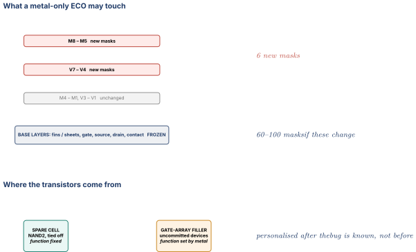
6.5 What a metal-only ECO can and cannot do
Be precise about the boundary, because "we did it with a metal ECO" invites exactly this follow-up.
It can rewire the connections between existing gates. It can personalise gate-array filler cells into new functions. It can connect a spare cell into a circuit. It can disconnect a gate and tie its input to a rail, which is how you disable a broken feature. It can insert buffering by wiring in spares. And it can change which of several existing signals feeds a mux, if the mux and the signals are already there.
It cannot create a transistor that does not exist. It cannot increase a cell's drive strength beyond what a nearby spare provides, because drive strength is a base-layer property. It cannot move a cell, and it cannot move or resize a macro or memory. It cannot change the fundamental structure of the clock tree, since the clock buffers are cells. And it cannot change anything about a hard macro's internals.
Three practical constraints bite even within the "can" list. Routing resource must exist on the changed layers in the region you need. A congested area may have no free tracks, and then the fix that is logically available is physically impossible. Timing of the patch is usually much worse than the original implementation would have been, because you are routing to wherever the spare happened to be rather than to where the tool would have placed a new cell. And the changed layers must independently re-close DRC and LVS, which at advanced nodes includes the multi-patterning colouring constraints of Part 7.4, so a metal-only patch can be illegal for a reason that has nothing to do with spacing.
6.6 How a timing ECO actually runs, step by step
This is the part you can speak to from experience, so it is worth having the sequence crisp.
One. The signoff timer reports violations, per view, sorted. You now have a list of endpoints and magnitudes.
Two, and this is the step that separates engineers. Triage each violation into real or not. A meaningful fraction of violations reported late in a project are not design problems at all: a missing or wrong timing exception, an input or output delay budget that no longer matches what the neighbouring block does, a constraint that was written for an earlier clock plan, an over-constrained path with a set_max_delay nobody remembers. Part 1.3 and Part 4.5 of note 20 are the reasoning for this. Fixing a constraint bug costs an hour. Fixing it with buffers costs area and power forever, on every unit shipped, and hides the real problem.
Three. For the genuinely real ones, generate a change list. Modern signoff timers will do this for you. They compute a set of resizes, buffer insertions and Vt swaps that they predict will close the violations, and emit it as a script the implementation tool consumes. The important property is that the signoff tool decides the fix, using its own accurate timing, rather than the implementation tool guessing with its faster, looser model.
Four. Apply it in the implementation tool in an incremental mode: place new cells in existing gaps, legalise so nothing overlaps, and route only the nets that changed, leaving every other route bit-identical. That bit-identical property is the whole point, because it is what makes the unaffected regions inherit their previous signoff results.
Five. Re-extract, and re-run timing across every view, not the one that reported the violation. This is the step people skip in an interview answer and it is the one that matters, because a hold buffer added to fix a fast-corner violation adds delay at the slow corner too.
Six. Re-run the other gates in Part 5 that the change could have disturbed. That means LEC always, DRC and LVS on the changed region, crosstalk if routing moved, and EM/IR if the cell mix in a region changed materially.
Seven. Repeat, with decreasing disturbance as in 5.7.
Two disciplines to volunteer, because they are the ones that come from having done it. Batch the ECOs. Each iteration costs a full extraction and a full multi-view timing run, so ten carefully-chosen changes in one pass is enormously cheaper than ten passes of one change, even though each individual change is easier to reason about alone. And fix setup before hold. Setup fixes move cells and change routing, which changes hold. Hold fixes are additive delay that rarely helps setup. Doing them in the other order means doing the hold work twice.
07.Part 7, what actually changes at 7 nm, 5 nm and 3 nm
7.1 The node number is a name, not a measurement
Say this first, because it is true, it is entirely public, and it immediately separates you from candidates who repeat marketing.
Up to roughly the 22 and 16 nanometre generations, the node name tracked a real drawn dimension, either the gate length or half the minimum metal pitch. It stopped doing so. At 7, 5, 3 and 2 nanometres, no drawn feature on the chip measures that. The name is a generation label indicating roughly where a foundry places a process on its own roadmap, and the labels are not comparable between foundries.
Four dimensions are meaningful, and a foundry will actually quote them. The contacted poly pitch is the spacing between adjacent transistor gates. The minimum metal pitch is measured on the tightest routing layer. The standard cell height is expressed as a number of routing tracks, so a "six-track library" is one whose cells are six metal pitches tall. And the resulting density is quoted in millions of transistors per square millimetre, for a stated mix of logic and memory cells.
Two consequences for you. First, a question like "have you worked at 7 nm" is really asking whether you have dealt with the design consequences below, not whether you memorised a number. Second, when comparing two foundries' offerings, the honest statement is that node names do not compare and the density and pitch figures do. That is a small, correct, checkable thing to say, and it reads as engineering rather than fandom.
7.2 FinFET, and the quantisation of drive strength
Here is the change that reaches a front-end designer most directly, and it is worth deriving rather than asserting.
In a planar transistor, the current the device can drive is proportional to its channel width , and is a drawn dimension. The layout designer can make it anything. That continuous freedom is what the standard cell library exploits. A library ships the same logical function at many drive strengths, X1, X2, X4, X8 and everything between, and synthesis picks whichever gives the best delay for the capacitance it presents. The optimisation is effectively over a continuum.
In a FinFET the channel is a vertical fin, and the gate wraps over its two sides and its top. The current now flows along all three of those surfaces, so the effective width of one fin is roughly
And here is the trap. and are set by the process, not by the designer. They are fixed by the etch and the deposition steps and are identical for every transistor on the die. The only way to get more drive is to put more fins in parallel.
Put illustrative numbers on it. Take a fin height of around 45 nm and a fin thickness of around 8 nm, which are in the right region for the finFET generations though the exact values are foundry-specific and are under the process design kit's non-disclosure terms:
So the available device widths are 100 nm, 200 nm, 300 nm, and so on. There is no 130 nm. If the optimal size for a path is 1.3 fins' worth of drive, you get one fin, which is 23 percent too weak, or two fins, which is 54 percent too strong and presents twice the input capacitance to whatever drives it.
Three consequences for the front-end designer, and they are the answer to "what changed for you."
The drive-strength ladder is coarse and the steps are large at the small end. Going from a one-fin device to a two-fin device is a 100 percent jump. Compare that to a planar library where the same functional step might be 30 percent. So "just upsize it" is a much blunter instrument, and the extra capacitance the bigger cell presents upstream frequently costs more than the drive it gained. That is why, at advanced nodes, buffering and restructuring beat sizing more often than they used to, and the fix order in Part 7.1 of note 20 shifts accordingly.
The optimisation problem became discrete. A tool optimising over a continuum can take small confident steps. A tool optimising over a coarse lattice has to make jumps, and small changes in the input can flip a decision that cascades. That is a real part of why advanced-node quality of results is noisier, and why re-running the same flow with a trivially different constraint can give a materially different answer. It is a genuinely non-obvious observation to offer.
The library got bigger and more specialised instead. With sizing coarsened, libraries compensate along other axes: multiple threshold voltages, multiple cell heights in the same design (tall fast cells for critical paths, short dense cells elsewhere), and many more logical variants of each function. So the tool's freedom moved from "how wide" to "which cell," and that is a combinatorially harder search.
7.3 Gate-all-around and nanosheets, and what they give back
The finFET's successor is the gate-all-around transistor, built as a stack of horizontal silicon nanosheets with the gate material wrapped completely around each one rather than over three sides. Intel's brand name is RibbonFET. The generic term used across the industry is nanosheet or GAA.
Public status as of the time of writing: Samsung announced volume production of its 2 nm class process in late 2025 and TSMC's N2 entered mass production in the fourth quarter of 2025, both using nanosheet devices. TSMC's N3 generation is still finFET. Intel 18A uses RibbonFET together with backside power. Treat specific yield and shipping claims as reported rather than confirmed, because those figures move and are contested.
The design-facing change that matters is the interesting one. In a finFET, the width knob was the number of fins, quantised in large steps. In a nanosheet device, the width knob is the drawn width of the sheet, which is a lithographic dimension again, so within some bounded range set by the process, width becomes continuous again. The number of stacked sheets is fixed by the process, so you get a continuous knob within a bounded range rather than free choice.
Hedge this appropriately, because the exact latitude is a process design kit detail and is not public. The defensible public statement is: nanosheet restores some of the width tunability that finFET removed, within limits the process sets, which relieves part of the quantisation pressure of 7.2 without eliminating it. Say that and stop. Do not claim to know a specific foundry's allowed sheet width range.
7.4 Multi-patterning, and the design rules it forces
This one seems like a manufacturing detail and is not, because it changes what a router is allowed to do, which changes what your RTL costs.
The first-principles problem. An optical lithography system can only resolve features down to a limit set by its wavelength and its numerical aperture. The immersion systems that carried the industry for a decade used 193 nm light, and with every available resolution enhancement they bottomed out at a minimum printable pitch, the repeat distance of a line-and-space pattern, somewhere around 80 nm. But the nodes needed 40 nm pitches and below.
The workaround. If one exposure cannot print lines at a 40 nm pitch, print two interleaved sets of lines at 80 nm pitch each, on two separate masks, offset by 40 nm. That is LELE, meaning litho, etch, litho, etch, also called double patterning. SADP, self-aligned double patterning, gets there differently: print a coarse sacrificial pattern called a mandrel, grow a conformal spacer film on its sidewalls, etch away the mandrel, and you are left with two spacer lines wherever there was one mandrel line, automatically at half the pitch and automatically self-aligned, which avoids the overlay error that LELE suffers. Do it twice and you get SAQP, quadruple patterning, at a quarter pitch.
EUV lithography, at a 13.5 nm wavelength, restores single-exposure printing at those pitches. It entered production around the 7 nm generation for a subset of layers and is used more broadly from 5 nm onward, which is why the multi-patterning burden shifted from "everywhere" to "the tightest layers that EUV does not cover, plus the layers where EUV double patterning is now itself needed."
Now the four design-rule consequences you actually meet.
Unidirectional routing. Multi-patterning of any flavour prints parallel lines, and it prints them well. It does not print bends. So each metal layer is restricted to run in one direction only, on a fixed pitch grid. Horizontal on one layer, vertical on the next, alternating. The consequence: every turn in a route costs a via, and vias have resistance and take area and have their own reliability rules. A route that would have been an L-shape on one layer in an older process is now two segments on two layers with a via between them. That is why via pillars, which are stacks of several parallel vias to reduce resistance and improve yield, became a real design object rather than a detail.
Colouring, and violations with no local cause. With LELE, every feature on the layer must be assigned to one of two masks, conventionally called two "colours", such that any two features closer together than the single-mask spacing limit are on different masks. Model the layer as a graph with an edge between every such close pair. The assignment exists if and only if the graph is two-colourable, which fails exactly when the graph contains an odd cycle. So three features mutually too close to each other, pairwise, is uncolourable, even though every individual spacing is perfectly legal on its own. That is a design rule violation with no local cause, since no single measurement is wrong, and it is the class of DRC error that most surprises people the first time. Standard cells arrive pre-coloured and the router must respect the colouring. A metal ECO can create a colouring conflict out of a change that looks trivially safe.
Cut masks and line-end rules. SADP and SAQP naturally produce continuous lines running the width of the pattern. To make a wire that ends somewhere, a separate cut mask removes a piece. But the cut mask has its own resolution limit, so there is a minimum spacing between cuts, which becomes a minimum spacing between line ends. Hence the proliferation of end-of-line rules, minimum area rules, and restrictions on where a wire may terminate relative to its neighbours.
Grid discipline generally. The net effect of all of the above is that advanced-node layout is far more gridded and restricted than older layout. Routers have less freedom, so congestion is less recoverable by cleverness and more determined by the connectivity you handed the tool. That is Part 8.7, and it is the reason a front-end engineer should care about any of this.
7.5 Wire resistance, and the delay balance that shifted under it
This is the single most consequential change for somebody writing RTL, and it is entirely derivable.
The geometric argument first. A wire's resistance is
where is width and is thickness. Scale a process by a factor , shrinking and together. The cross-sectional area falls as , so resistance per unit length rises as .
Capacitance per unit length, meanwhile, is roughly scale-invariant, because it is set by ratios of geometry, namely how wide the wire is relative to how far it sits from its neighbours, and scaling preserves ratios. So per unit length rises as .
Now work two cases and notice they differ.
A local wire shrinks with the layout, so its length also scales by . The delay of a distributed line goes as (resistance per length) (capacitance per length) , so
A global wire crossing the die does not shrink, because the die does not shrink. You fill it with more logic instead. So is constant and
Meanwhile gate delay, under classical scaling, falls roughly as . So the ratio of wire delay to gate delay grows as for local wires and as for global ones. Local wires get relatively worse. Global wires get catastrophically worse. That is the whole memory of why the industry moved from "wires are free" to "wires are the problem," and it is the analytic content behind Part 8.6 of note 20.
Then it gets worse than geometry predicts, for two additional physical reasons.
Resistivity itself rises. Copper's bulk resistivity assumes electrons travel freely between scattering events over a characteristic distance, the mean free path, commonly quoted at around 40 nm in copper at room temperature. Once the wire's cross-sectional dimensions fall below that distance, electrons start scattering off the wire's surfaces and off grain boundaries, which shrink with the trench. The effective resistivity therefore climbs above bulk, and published measurements show it rising sharply as linewidths fall into the sub-10 nm region.
The barrier eats the cross-section. Copper diffuses into silicon dioxide and poisons transistors, so every copper wire needs a diffusion barrier and an adhesion liner around it, historically a tantalum-nitride and tantalum stack. That stack needs to be a few nanometres thick to work regardless of how narrow the wire is, and it is far more resistive than copper. So as wires shrink, the barrier occupies a growing fraction of the cross-section.
Work the arithmetic with a 3 nm barrier on each side, which is in the published range:
| Drawn wire width | Copper width | Copper fraction of width |
|---|---|---|
| 100 nm | 94 nm | 94 percent |
| 40 nm | 34 nm | 85 percent |
| 20 nm | 14 nm | 70 percent |
| 12 nm | 6 nm | 50 percent |
And accounting for the barrier under the wire as well, the area fraction is worse still. Published work on sub-10 nm interconnects reports that copper occupies only around 30 percent of the total cross-sectional area at a 10 nm linewidth. So the effective resistance of the smallest wires is several times what the geometric argument alone predicts.

The consequences for a front-end designer, which is the payoff.
A long net stopped being a wire and became a delay element with a budget. Global signals need repeater chains, repeaters need silicon area and burn dynamic power and must be placed somewhere, so a signal's route is now a floorplan negotiation. A growing fraction of a block's total instance count is buffers that compute nothing.
Structurally, the architecture moves toward locality. Clustered execution units with local bypass networks and a slower path between clusters, per Execution Units. Banked caches with non-uniform access latency instead of one flat array. Registered pipeline slices inserted into an interconnect purely to break a wire, per Interconnect and AMBA, which are pipeline stages that exist for no logical reason at all. And, at the largest scale, there are chiplets. If crossing a big die is expensive anyway, you may as well cut the die up and pay an explicit, engineered, characterised cost at the boundary instead of an implicit one in the middle.
Industry's response on the physics side is worth naming in one sentence: cobalt and ruthenium have been introduced as liner or fill materials at the tightest layers because they behave better than copper at small dimensions despite higher bulk resistivity, and research into topological semimetals and other alternative conductors is active. Do not claim more than that.
7.6 Variation stops being a correction and becomes a first-order effect
Three mechanisms compound, and the reason to know them is that they are why the POCV and LVF machinery of Part 3.4 became mandatory rather than optional.
Random dopant fluctuation. A transistor's threshold voltage depends on the dopant atoms in its channel. As the channel shrinks, the number of those atoms falls, and the statistics of a small count are proportionally noisier than the statistics of a large one, since the relative fluctuation of randomly placed atoms goes as . Halve the channel volume and the relative spread grows. This was one of the arguments for finFET in the first place, since an undoped or lightly doped fin channel with the gate controlling it electrostatically is much less exposed to it.
Line-edge roughness. The edge of a printed feature is not a straight line. It wanders by an amount set by the photoresist chemistry, which is roughly a fixed absolute magnitude. Against a 100 nm feature, a 2 nm wander is 2 percent. Against a 15 nm feature it is 13 percent. The noise did not grow. The signal shrank.
Local layout effects. Mechanical stress from neighbouring structures, proximity to a well edge, and the density of surrounding patterns all shift a device's behaviour. These are systematic rather than random, in that the same layout gives the same shift, but they are not captured by a corner, and they mean two instances of the same cell in different neighbourhoods genuinely differ.
The consequence is that the ratio for a single cell's delay grows generation over generation. The whole argument in Part 6.5 of note 20, that pessimism is paid for in area and power on every path in every unit shipped, gets sharper as the pessimism required by a blanket derate grows. That is why AOCV, POCV and LVF moved from advanced technique to table stakes.
Two related effects belong to the same family and are covered in Reliability Aging and Variation. Aging, principally bias-temperature instability and hot-carrier injection, shifts thresholds over a part's operating life, so timing must be signed off against an end-of-life library as well as a fresh one. Self-heating became significant in finFETs and nanosheets because the device sits on a thermally poor path to the substrate and its local temperature can run well above the die average.
7.7 Backside power delivery, the one that solves two problems at once
The newest structural change, and the one to describe as a trend rather than as something you have used.
Conventionally, power and signals share the same metal stack on the front of the wafer. Power comes in at the bumps on top and works its way down through a dozen or more layers to the transistors, and the wide power straps it needs on every layer consume routing resource that signals wanted.
Backside power delivery moves the power network to the back of the wafer, connected to the transistors through vias etched through the thinned silicon. Intel's implementation is called PowerVia and ships on the 18A process. TSMC's implementation, called Super Power Rail, is on its A16 roadmap for roughly the 2026 to 2027 window. Treat both schedule claims as publicly announced roadmaps rather than as fact.
It buys two things simultaneously, which is unusual. IR drop improves sharply, because the path from the package to the transistor is short and wide instead of long and thin. Intel published a test vehicle at VLSI 2023. It was a modified Intel 4 process carrying x86 efficiency cores at 1.1 V and 3 GHz, built once with and once without the backside network, and Intel reported roughly a 30 percent reduction in IR droop, about a 6 percent improvement in maximum operating frequency, and about a 20 percent reduction in signal wire length on the top metal layers. Quote those as their published test-chip figures on one specific process, not as a general number for the technique. The honest framing is "Intel reported about a thirty percent droop reduction on their PowerVia test vehicle," and do not convert it into an absolute before-and-after percentage of the supply, because they did not publish it that way. And routing resource is freed, because the front-side layers no longer carry power straps, which directly relieves the congestion of Part 8. That is what that 20 percent wire-length figure is measuring.
Note what that means for the two problems above. Better IR means less voltage-induced delay degradation and less dynamic droop, which is margin recovered. Freed routing means the wire-resistance pressure of 7.5 is partly offset by having more tracks available on the layers that were most congested. It is one of the few changes in recent years that helps in both directions at once, which is why every leading foundry is doing it.
7.8 The paragraph to have ready
Compress the whole part into something speakable, because the question "what changes at advanced nodes" is asked constantly and rambling through seven mechanisms loses the room.
"Four things change and they all point the same way. Device sizing became quantised, so upsizing is a blunt instrument and restructuring beats sizing more often than it used to. Lithography forced unidirectional gridded routing with colouring constraints, so the router has much less freedom and congestion is decided more by my connectivity than by their placement. Wire resistance rose faster than geometric scaling predicts, because the barrier eats the cross-section and electrons scatter off surfaces below the mean free path, so long nets are now delay elements with budgets and locality became an architectural constraint rather than a preference. And variation went from a correction to a first-order effect, which is why signoff needs POCV with real LVF data rather than a flat derate. The single sentence is: at advanced nodes my structural choices in RTL, especially how much stuff has to talk to how much other stuff, cost more than my logic depth does."
That last sentence is the one that lands, and it is the bridge into Part 8.
08.Part 8, floorplan vocabulary a front-end engineer meets in a review
8.1 Why a front-end engineer is in this meeting at all
You will not run the floorplanning tool. You will sit in a review where somebody shows a coloured picture of your block and says things about it, and what you need is to understand the picture well enough to know when the answer is "that is my problem and here is what I will change in the RTL."
That is the correct scope and it is worth stating explicitly in an interview, because claiming to be a physical designer when you are not fails on the first follow-up, while saying "I know what those numbers mean and I know which of them I can move" is both true and valuable.
8.2 Utilisation, and why you cannot run at 95 percent
Utilisation is the fraction of available area occupied by cells. Work it.
A block has a core area of 1000 µm by 1000 µm, so . Summing every standard cell instance's area gives . Then
The immediate question is why you would not push that to 95 percent and buy back a third of the die. Four reasons, and each one is a thing that has to physically fit somewhere.
Routing needs the space above the cells, and needs the cells not to be packed. Wires run in the metal layers above, but they must get down to the cells' input and output pins, and a pin buried in the middle of a solid wall of cells may have no accessible track above it. Pin access is a first-order problem at advanced nodes precisely because of the gridded unidirectional routing of Part 7.4.
Clock tree synthesis has not happened yet. CTS inserts a large number of buffers, and they have to go near the flops they drive, which is exactly where it is already crowded. A floorplan with no room where the clock tree needs to be forces the buffers somewhere else, which means longer clock wires, which means more skew, which is the thing CTS exists to control.
Optimisation and ECO need gaps. Every buffer inserted to fix a slew violation, every hold buffer, every upsized cell that grew, and every ECO from Part 6 needs a legal placement site adjacent to where it logically belongs. A block with no gaps cannot absorb a fix without a re-placement, which is exactly the disturbance you cannot afford late.
Spare and gate-array cells from Part 6.4 occupy area on purpose.
So the opening utilisation is chosen with headroom, and the number depends heavily on how much routing the block demands. Figures in the 60 to 75 percent region are commonly used for logic-dominated blocks, lower for very congested ones and higher for regular datapath-like ones. Treat those as ranges, since they vary enormously by company, node and block type.
One pedantry that matters in a review: ask which definition is being quoted. Some tools report utilisation against the total core area including macro footprints and placement blockages. Others report it against the area actually available for standard cells after macros and blockages are subtracted. Those two numbers can differ by twenty points on a macro-heavy block, and two people quoting different definitions at each other is a routine source of confusion.
8.3 Congestion, with the mechanism worked out
Congestion is the word that will be aimed at you, so understand it mechanically rather than as a colour on a map.
The router divides the die into a grid of global routing cells, usually called gcells. Think of a tile a few microns on a side. For each tile, the tool computes two numbers: the supply, meaning how many wire tracks can physically cross that tile, and the demand, meaning how many nets need to cross it. The difference is the overflow.
Work it with numbers. Take a gcell of 5 µm by 5 µm and a routing pitch of 100 nm on the layers in question. That pitch is a round figure for illustration, and advanced nodes are considerably tighter. Then one metal layer running horizontally can carry
If the block has six usable routing layers, three running horizontally and three vertically, the tile supplies 150 horizontal tracks and 150 vertical. Now subtract what is not available: power straps take some, the clock takes some with its extra spacing and shielding, and pin access takes some. Call the usable horizontal supply 120.
If the global route says 145 nets must cross that tile horizontally, the tile has an overflow of 25. Those 25 nets cannot go through, so the router detours them around, which makes them longer, and their detour consumes tracks in the neighbouring tiles, which may push those into overflow too.
That mechanism gives the two properties that make congestion feel the way it does. It is local, so a block can be 62 percent utilised overall and completely blocked in one 20 µm square. And it is contagious, because relieving one tile pushes demand outward, which is why congestion problems spread when you poke them and why a "small" fix in a congested region can make things worse.
What it costs when it is not fixed: detoured nets are longer, so they are slower and burn more power, and their timing is unpredictable until routing is done, which destroys the correlation between pre-route and post-route timing. If the router genuinely cannot complete, you get DRVs, the design rule violations left in the routed database, such as shorts and spacing violations. A database with unresolved DRVs cannot be signed off at all.
The vocabulary: gcell, overflow, congestion map and hotspot, global route congestion often shortened to GRC, detour, DRV, and "the design does not route," which is the phrase you do not want to hear about your block.
8.4 Macro placement, and the RTL decision hiding inside it
Macros are the hard blocks: SRAM instances, register file arrays, PLLs, analogue IP, PHYs. They are fixed rectangles that the tool cannot reshape, with pins on specific edges at specific pitches, and they are usually placed by hand or with heavy human guidance because their placement determines almost everything else.
Three things a macro does to a floorplan. It blocks the area it occupies, and usually a halo or keep-out margin around it as well, so standard cells cannot go there. It blocks routing on the layers it uses internally, so nets crossing the block must go over it on higher layers or around it. And its pins are on one edge, so the logic that talks to it wants to be on that side, which pins down a chunk of the placement.
The rules of thumb are simple and they are worth being able to state. Push macros toward the periphery so the middle stays a contiguous field for standard cells. Orient their pins toward the logic that uses them. Leave routing channels between and around them wide enough for the nets that must cross. And avoid creating narrow canyons of standard-cell area between macros, because cells placed in a canyon have no routing escape and become a congestion hotspot by construction.
Now the front-end connection, which is the reason this section exists. How many memory instances your design contains, and how you bank them, is an RTL decision that lands directly on the floorplan. Instantiating one 32 KB memory gives the floorplanner one large rectangle to place. Instantiating four 8 KB banks gives four smaller ones that can be distributed, but it also gives four sets of address and data buses that all need routing, and four sets of control logic. Which is better is a real trade-off with a real answer for a given block, and it is decided by an RTL engineer, months before anybody opens the floorplan. Being able to say "I chose four banks rather than one because the block's aspect ratio was going to force a long haul otherwise, and I checked that with the physical designer before I wrote it" is a very strong thing to be able to say.
8.5 Pin placement, and the other half of the budget negotiation
A block's pins, the ports on its boundary, have to be assigned to physical locations on that boundary. The consequence is direct. If a 128-bit bus's pins are on the left edge and the logic that consumes it ends up on the right, all 128 bits cross the entire block, consuming tracks all the way and arriving late.
The vocabulary you meet includes pin assignment, also called port placement. It includes feedthrough, a net that enters a block and leaves again without being used inside, which happens when the top-level routing is easier through your block than around it and which you may be asked to accept. And it includes pin density, since pins on a boundary compete for the same limited edge tracks.
The connection to note 20 is worth making explicitly because it is a nice piece of joined-up thinking. Part 3.3 of STA Synthesis and Physical Design describes the input and output delay budget negotiation between neighbouring block owners, meaning how much of the cycle each side gets. Pin placement is the physical half of the same negotiation. A generous timing budget on a pin placed at the far corner of your block is not generous at all, because the wire from the pin to the logic eats it. Agreeing the number without agreeing the location is how a block closes standalone and fails at integration.
8.6 Bumps and RDL
This is the top of the physical stack and a front-end engineer meets it rarely but should recognise the words.
In a flip-chip package the die is turned face down and connected to the package through an array of solder bumps distributed across its whole face, rather than through wire bonds at the edges. The classical bumps are called C4, controlled collapse chip connection. The finer-pitch versions used in advanced packaging are called microbumps. Bump pitch is coarse compared with on-die metal, tens of microns rather than tens of nanometres.
The redistribution layer, or RDL, is the topmost thick metal layer whose job is to route from wherever the die's I/O and power connections naturally are, out to wherever the bump array wants them. It exists because the on-die layout's convenient positions and the package's convenient positions do not coincide, and it is essentially a small, coarse routing problem of its own that can itself be congested.
Two consequences a designer should know. First, power enters the die at the bumps, so the IR drop map of Part 5.4 is fundamentally a function of where the power bumps are. A region of the die far from a power bump droops more than one directly under a cluster of them, and the bump map is therefore a power-integrity input rather than a packaging detail. Second, high-speed I/O bump placement constrains where the corresponding PHY macros can sit, because the connection from the PHY to its bumps has to be short and controlled. That is why a memory PHY of the kind in DRAM Controllers JEDEC and DFI sits on a die edge under its bump field, and why moving it is not a floorplan preference but a package re-design.
8.7 Why your RTL shows up as congestion
Now the section that makes the whole part worth reading, because it is the one an interviewer is actually probing when they ask about physical awareness.
Congestion is, to first order, a property of the connectivity graph you wrote, not of where the tool put things. Placement can redistribute congestion. It cannot remove connectivity. If a region of your design requires wires to converge on a small logical structure, those wires exist regardless of where the structure is placed, and if is large enough relative to the area the structure occupies, no placement is good.
The structures that do it, with the mechanism rather than just the name:
Crossbars and all-to-all connections. An crossbar has, by construction, paths. A 16-by-16 crossbar of 64-bit words is wire-bits converging on one region. That is congestion built into the specification. The mitigations are architectural, and they are RTL decisions. Reduce the radix, go hierarchical with two smaller stages, or serialise over fewer wires and pay latency.
Register files with many ports. Each read port is a full-width bus leaving the array and each write port a full-width bus entering it. A 128-entry, 64-bit register file with eight read and four write ports has twelve 64-bit buses on its boundary plus the address and enable lines, all converging on a small dense array. Port count is the dominant term in a register file's area and its congestion, which is why banking, clustering and port reduction are recurring microarchitectural moves in Execution Units.
Broadcast nets. A flush, a stall, or a global enable fanning out to several thousand flops becomes a buffer tree that occupies area throughout the block and routes everywhere. Its own congestion contribution is modest, but it is present in every region simultaneously and it is on a timing-critical path in many of them. Pipelining a broadcast so it arrives a cycle later in distant regions is a microarchitectural fix to a physical problem, and knowing it is available is worth a lot.
Wide multiplexers with far-apart inputs. A 12-to-1 mux of 64-bit values pulls twelve 64-bit buses from wherever their sources are into one place. If the sources are spread across the block, the mux is a congestion magnet whether or not the mux itself is large.
Aggressive resource sharing. Synthesis can share one adder among several logically distinct additions, which saves area, and it does so by routing every operand set from every site to the shared adder and the result back to every consumer. Part 2.2 of note 20 flags this as a trade-off. The physical cost of the trade-off is exactly this.
And the counter-example, which is the useful half. Structures with local, regular, short connectivity route beautifully at any utilisation. Examples are a pipelined systolic array where each stage talks only to its neighbour, a banked structure where each bank has its own local control, and a datapath where bit talks mostly to bits and . That is why bit-sliced and array-structured designs are physically friendly, and it is a genuine design principle rather than an aesthetic preference.
The sentence to have ready for the review meeting: "congestion is usually a connectivity property of the RTL, so placement can redistribute it but not remove it. Tell me which region and I will tell you which structure is causing it." That sentence turns the meeting from a complaint into a collaboration, which is exactly the behaviour the question is testing for.
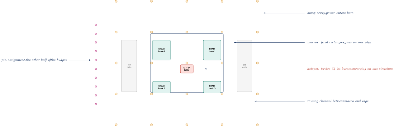
09.Part 9, how to talk about STA flow ownership in this vocabulary
9.1 What you genuinely have, translated
Your record includes RTL design, synthesis, and static timing analysis flow ownership, plus a group-wide upgrade of a lint and physical verification flow. That is real and it is more than most candidates at your band have. The problem is not the substance, it is that the sentence "I did synthesis and timing closure" reads identically whether the person did it for four years or read about it for four hours.
So translate it into the vocabulary this note has built. The translation is not embellishment. Every clause below is the same fact stated in the register the listener is sampling for.
Instead of "I owned STA for my block," the shape is: "I owned the constraint set and timing closure for a block of roughly instances at gigahertz. I wrote and maintained the SDC, I owned the exception list and the justification for every entry on it, I drove synthesis quality of results, and I closed timing across our signoff view list working with the physical design team."
That sentence commits to five checkable things. They are instance count, frequency, constraint ownership, exception ownership and view list, and each one is an invitation to a follow-up you can answer. Which is the point.
Then be ready for the five follow-ups it invites.
"How many views?" Give the number, and give the structure: how many modes, how many corners, which axes, and roughly how it was pruned. If your flow was smaller than the 945-scenario example in Part 2.4, and most block-level flows are, say the real number. A candidate who says "twelve, because we had three modes and four corners and the hold analysis reused two of them" is far more credible than one who says "lots."
"Which tools?" Name the ones you used, in the class structure of Part 4. Do not name the ones you did not.
"What did your timing look like at the end?" WNS, TNS, number of failing endpoints, and the shape argument from Part 5.5 of note 20. Was it one bad path or a distribution.
"What was the hardest path?" Part 9.2 below.
"Any waivers?" If there were, be able to say what they were and why they were defensible. If there were none, say so, because that is a good answer.
9.2 The three stories to have loaded
The scope story, above, delivered in one breath.
The hardest path story. Not "I closed timing on my block" but a specific path: where it started and ended, why it was long, what you checked before spending area, what you actually did, and what it cost. Part 7.2 of note 20 works exactly this shape. The reason it matters is that it is unfakeable. A person who closed a real path remembers the structure that caused it, and a person who did not, cannot invent one that survives two questions.
The judgment story, which is the one to lead with if you get to choose. The time a reported violation turned out not to be a design problem at all. A missing multicycle exception. An input delay budget that no longer matched what the neighbouring block actually did. An over-constrained path with a set_max_delay that somebody added for a reason that had expired. The narrative is: it was reported as a violation, I did not immediately fix it, I proved what it actually was, and the fix was a constraint change rather than silicon.
That story is worth more than the hardest-path story, for a reason worth naming out loud: buffering a path that was never really failing costs area and power in every unit shipped, forever, and hides the actual problem. Somebody who reaches for the constraint file before the buffer has the judgment the role needs. This is also where your formal verification background connects, and the connection is genuine rather than stretched. An unproven timing exception in an SDC file and an over-broad assume in a formal property are the same failure mode, an unverified assertion that silently removes a real case from analysis. Saying that sentence in an interview is a strong, specific, non-obvious signal, and it is already flagged in Part 10 of note 20 for the same reason.
9.3 The flow-upgrade credential, framed properly
The lint and physical verification flow upgrade is the rarer credential and the one most likely to be under-sold, because it sounds administrative. It is not. Most RTL engineers consume a flow. Very few improve one, and the difference is exactly the difference between somebody who can be handed a methodology problem and somebody who cannot.
Frame it with the economics in Part 9.5 of note 20: what class of bug the upgrade catches, at what stage it now gets caught instead of where it used to get caught, and what that stage difference is worth. A bug found by lint costs an hour. The same bug found at signoff costs weeks. The same bug found in silicon costs a re-spin, and Part 6.3 of this note gives you the number to attach to "re-spin."
That framing turns "I helped improve our lint flow" into "I moved a class of defect from signoff-stage to RTL-stage detection across a group, and the difference between those two stages is weeks per occurrence." Same fact. Entirely different weight.
9.4 What not to claim
Be explicit with yourself about the boundary, because the whole value of this note evaporates if you cross it.
Do not claim to have owned place and route, clock tree synthesis, EM and IR signoff, or physical verification if you consumed their outputs. The correct posture is that you know what each check proves, who owns it, and what it asks of you as a block owner. That posture is strong. Overclaiming here is the single easiest way to lose an interview you were winning, because the physical designer on the panel will ask one question and know.
Do not claim POCV or LVF experience if your flow used flat derate. Say that you know why the pessimism exists and derive the argument from Part 6.4 of note 20, which demonstrates the understanding without the claim.
Do not claim advanced-node experience you do not have. Everything in Part 7 is published-literature knowledge and should be presented as such: "that is my understanding of what changes and why, from the published material. I have not personally taped out at that node."
Do not name a tool option, a command switch, or a version-specific behaviour. Describe what the step accomplished.
And the positive form of all four, which is the sentence to actually use: "I know what that check proves and who owns it" is a strong answer to a question about work you did not do. "I ran that" when you did not is a trap that closes on the next question.
10.Part 10, the interview questions, with answers
Fifteen questions of the kind actually asked when a role screens on this vocabulary, each with a model answer written the way a strong candidate would speak it rather than the way a reference manual would state it, the follow-up the interviewer will reach for next, and the trap where there is one. Read them out loud. They are calibrated to be spoken in one to three minutes, which is the real constraint.
Q1. What is the difference between a mode and a corner?
Model answer. A mode is a functional configuration and it is defined by its own constraint file. Functional operation, scan shift, scan capture, at-speed test, memory BIST and a retention configuration each have their own clock definitions, their own exceptions, and often a different effective connectivity because muxes sit in different positions. A corner is a manufacturing and operating condition plus the electrical data that describes it: a process point, a voltage, a temperature, and an interconnect extraction condition, which together decide how fast every cell and every wire is.
The clean test I use is: if the SDC changes, it is a mode, and if only the libraries and the parasitics change, it is a corner. Two operating frequencies of the same logic are two modes, because create_clock names a different period. Two supply voltages at the same frequency are two corners, because the constraints are identical and only the characterisation differs.
The reason it matters is that they are not redundant with each other. A mode can give a qualitatively different answer, not just a scaled one. Scan shift is the example I would give. Setup in shift passes with enormous margin, because the shift clock is maybe twenty times slower than the functional one and the logic between adjacent scan flops is a single multiplexer, which is seventy picoseconds of arrival against a requirement near ten nanoseconds. But hold in shift is one of the hardest checks in the whole design, because the hold equation has no period in it, the logic depth is minimal, and the chain is stitched for physical convenience so the clock skew between adjacent flops can be large. So you cannot pick the worst mode and run only that. There is no worst mode.
The follow-up. "So how many of each do you have?"
Give real numbers and the structure. Seven or eight modes is ordinary. On corners, name the axes rather than a single count: process, voltage, temperature, and interconnect, and note that the interconnect axis alone has four or five positions.
The trap. Saying a mode is "a different frequency" and a corner is "a different PVT." The first half is nearly right for the wrong reason and the second half misses interconnect entirely, which is the axis that surprises people and is the one Q4 goes after.
Q2. What is MMMC, and how many scenarios does a real block have?
Model answer. Multi-mode multi-corner. A scenario, or a view in Cadence language, is one mode paired with one corner, and it is the unit of work. One scenario is one complete timing analysis over every endpoint in the design.
The reason it is a named discipline rather than a detail is the arithmetic. Take seven modes, three process points, three voltages from the DVFS table, both temperature extremes plus nominal, and five interconnect corners. The naive cross product is , which is 945 scenarios. If one scenario is two hours on a compute node, a full pass is nearly nineteen hundred CPU-hours, which is about seventy-nine days serial, and you need several passes a day during closure.
But the compute is not what actually shapes the schedule. The thing that does is that every fix has to be re-checked against every scenario. A buffer added to fix setup at the slow corner also exists at the fast corner, where it may create a hold violation, and downsizing to fix that may reopen the setup problem. With one scenario that loop converges in an afternoon. With hundreds it does not converge on its own, which is why the flow is built around a small driver set during implementation and the full pruned list at signoff.
The follow-up. "How does the tool handle that many?"
They are run concurrently in one session rather than as independent jobs, so a proposed fix can be evaluated against all of them at once. Synopsys's mechanism for that is publicly called distributed multi-scenario analysis, DMSA. On the Cadence side the configuration is built up as library sets, RC corners, delay corners, constraint modes and analysis views, saved in a view definition file. I would describe the structure rather than the syntax, because the syntax is version-specific and I would not want to quote it from memory.
The trap. Quoting 945 as though it were a signoff list. It is the naive cross product and nobody runs it. The whole engineering content is in what you cut, which is Q3.
Q3. Your naive scenario list is 945. Cut it. Defend the cut.
Model answer. Four arguments, in decreasing order of how safe they are, and then a structural move.
Impossible combinations are free. The cross product contains conditions the silicon is never in. MBIST does not run at the turbo voltage because turbo is a thermally-managed boost condition, not a test condition. Scan shift does not run at the lowest voltage because shift happens on a tester at a nominal setting. The low-power functional mode does not exist at the top voltage because the whole premise of that mode is that the rail dropped. Each of those deletes a whole slab, and none of them costs anything, because I am not declining to analyse a condition, I am observing that the condition does not exist.
Setup and hold split the list. Setup binds at the slow end of the space and hold at the fast end, so most scenarios can be enabled for one check rather than both. Temperature inversion complicates it. At low supply the threshold effect can outweigh the mobility effect and the cold corner becomes the slow one, so the low-voltage entries genuinely need both temperature extremes even though the high-voltage ones may not.
Interconnect corners get chosen against what the block contains. A short capacitance-dominated net is worst at maximum capacitance. A long resistance-dominated net is worst at maximum product. If my longest net is two hundred microns, I do not need the same list as a block with a millimetre-long bus. That is a local, checkable argument.
Dominance, used carefully. If one scenario is slower than another on every path in a group, the faster one cannot report a setup violation the slower one misses. I would be cautious here, because cell delays do not scale uniformly across a library. A PMOS-limited transition and an NMOS-limited transition move differently between corners, so I would make the dominance argument per path group rather than globally.
And the structural move: run a small driver set of maybe four to eight views during implementation, chosen because they bind, and the full pruned list of twenty to forty at signoff.
The follow-up. "What if you cut wrong?"
Then the chip fails at a condition nobody analysed, and the failure shows up as parts that work at room temperature and fail at one voltage-temperature combination, months later, and it is close to untraceable. That is why the list has a named owner, why every deletion has a written justification rather than a remembered one, and why it gets re-audited whenever the DVFS table, the library, the test methodology or the floorplan changes. Scenario reduction is a risk decision, not an optimisation, and treating it as an optimisation is how you get a silent failure.
The trap. Reaching for dominance first, because it sounds the most technical. It is the weakest of the four arguments and the hardest to actually prove. Leading with the impossible combinations shows you have thought about what the product does rather than about what the tool does.
Q4. Why are there four or five interconnect corners rather than two?
Model answer. Because and move in opposite directions with process variation, and different nets care about different combinations.
Thicker, wider metal has lower resistance and higher capacitance, because there is more surface facing the neighbours. Thinner, narrower metal has the reverse. So there is no single "bad metal" condition.
Work it. Take a small driver with about two kilohms of output resistance. A short net with five femtofarads and a hundred ohms is dominated by the driver charging the capacitance, since the driver term is forty times the wire's own term, so it is worst at maximum capacitance and resistance barely participates. Now take a long net at eighty femtofarads and four kilohms. There the driver term and the wire's own term are about equal, and if I move to a condition that raises resistance by twenty-five percent and capacitance by ten, I get a larger delay than at the maximum-capacitance condition, because I made the dominant term worse. So the corner that is worst for the short net is not worst for the long one.
That is why the foundry supplies a set: a maximum-capacitance corner and a minimum-capacitance corner for the short nets, plus corners that maximise and minimise the product for the long ones, plus a typical for correlation. The names are broadly Cworst, Cbest, RCworst, RCbest and typical, though the exact set and the exact definitions come with the process design kit and vary by foundry, so I would check the kit rather than quote a list from memory.
The follow-up. "What does adding an interconnect corner cost you compared with adding a voltage?"
Much more. A voltage is another set of .lib files that already exist in the kit. An interconnect corner is a full re-extraction of the routed design producing another SPEF, which is a multi-hundred-megabyte parasitic database, plus the disk and the runtime to carry it in every timing run. That asymmetry is a real driver of which axis gets pruned first.
The trap. Saying there are two, a best and a worst. That is the answer of somebody who has heard the concept and not used it, and it has no answer to the follow-up, "worst for what net?"
Q5. What is on-chip variation, and what do AOCV, POCV and LVF add?
Model answer. A corner captures die-to-die variation, meaning that this whole die came out slow. It captures nothing about the fact that two nominally identical inverters a hundred microns apart on the same die differ, because of random dopant fluctuation, line-edge roughness, and local layout effects like stress and well proximity. So on-chip variation is a second mechanism layered on top of corners.
The crude implementation is derating. Make everything on the launch path a few percent slow and everything on the capture path a few percent fast, so you assume the worst combination. That is safe and it is badly pessimistic for two separate reasons. First, the two clock paths share physical buffers before the tree branches, and a blanket derate asserts that the same buffer is simultaneously slow and fast, which is not conservatism, it is nonsense, and common path pessimism removal credits that back. Second, random variation averages along a path. If each stage has a relative variation , then independent stages give a path variation of , so a twenty-stage path should be derated about four and a half times less than a one-stage path. A flat derate applies the single-stage figure to everything.
AOCV replaces the single number with a table indexed by path depth and by the physical span of the path, which captures both effects approximately. POCV goes statistical. Each cell carries a mean and a standard deviation, the tool combines them as random variables along the path, and slack is reported at a chosen sigma, usually three. The library data that makes POCV possible is carried in LVF, Liberty Variation Format, which is the .lib extension holding per-arc variation moments. At advanced nodes it carries higher moments than mean and sigma, because the distributions get skewed.
The follow-up. "Which did your flow use?"
Answer honestly, and if the answer is flat derate, say so and then say why the pessimism matters. Every picosecond of unjustified margin has to be bought back with upsizing or low-Vt swaps, which cost area and multiply leakage, on every path, in every unit shipped. Knowing why the recovery is worth money is more valuable than having pressed the button.
The trap. Saying POCV is "more accurate" and stopping. The interesting statement is that POCV is only as good as the LVF data behind it, so running POCV against a library that was not characterised for variation gives precision without accuracy. Volunteering that is a strong signal.
Q6. Name the checks that gate a tapeout, and say what each proves that the others do not.
Model answer. I would group them and be explicit that they are gates that must all hold on the same database version, not a pipeline.
Timing, across every view: setup, hold, recovery and removal on asynchronous resets, minimum pulse width, and clock-gating checks, plus the electrical rules on transition, capacitance and fanout. Proves the design meets its clock at every analysed condition.
Noise, meaning crosstalk: delta delay, which is what coupling does to arrival times, and glitch, which is what coupling does to a net that is supposed to be sitting still. Proves that the timing numbers survive the neighbours switching, which ordinary STA assumes away.
Power integrity: static IR drop, dynamic voltage drop, and electromigration on both power rails and signal nets. Proves the delivery network can actually supply the current without the local rail sagging below the voltage the timing analysis assumed.
Physical verification: DRC proves the geometry is manufacturable and says nothing about correctness. LVS proves the geometry implements the intended netlist and says nothing about manufacturability. Antenna proves no gate oxide was damaged by plasma charging during the build, which is a check about the manufacturing sequence rather than the finished object. Density and fill proves polishing will work, and matters to timing because fill adds capacitance and therefore has to be inserted before the final extraction.
Logic equivalence proves the netlist computes what the RTL computes, formally rather than by simulation. DFT proves the part is testable, with ATPG coverage and chain integrity. Power intent proves the domain structure, isolation, level shifting and retention are right, which needs both static checks on the structure and power-aware simulation on the sequencing.
The follow-up. "Which one would you expect to be the last one to close, and why?"
Timing, usually, but the interesting answer is that it is not any single one. It is the interaction. Widening a strap for EM displaces routes, which changes both delay and coupling, which needs a timing ECO, which adds cells, which changes the current profile, which reopens EM. What makes that converge is a discipline of decreasing disturbance: early iterations can re-place and re-route, later ones can only insert buffers in existing gaps, and the last ones can only resize a cell in place. That is what the sequence of freeze dates on a schedule is actually encoding.
The trap. Naming DRC and LVS and stopping, or conflating them. The single best discriminator in this whole answer is being able to say that DRC says nothing about correctness and LVS says nothing about manufacturability, because that shows you know why they are two checks rather than one.
Q7. What is crosstalk signoff and why is it not just static timing analysis?
Model answer. Because ordinary STA analyses each net in isolation, and once wires are tall, thin and close together, a net's capacitance to its neighbours is comparable to its capacitance to ground. Then what the neighbour does changes what this net does, and the isolation assumption is no longer safe.
Two effects, with the aggressor and victim vocabulary. Delta delay: if the aggressor switches the same direction as the victim at the same moment, it drags the victim along through the coupling capacitance and the victim arrives early. If it switches the opposite way, it fights and the victim arrives late. So the same physical net has two delays depending on its neighbour, and the spread can be a large fraction of the nominal. Note that both directions are dangerous. Opposite-direction coupling is a setup risk and same-direction coupling is a hold risk.
Glitch, or noise: the victim is not switching, it is being held at a rail, and the aggressor's transition couples a bump onto it. If the bump crosses the receiver's threshold and lasts long enough it propagates as real logic, and if it reaches a flop's data pin in the capture window it is captured. If the victim is a node with nothing holding it, such as a dynamic node or a floating node in a powered-down region, the disturbance just stays there.
The reason it needs its own analysis mode rather than being folded into the timer is that it is iterative. To know whether an aggressor is credible you need the timing windows, but the coupling changes the delays, which moves the windows, which changes which aggressors are credible. So the tool loops to a fixed point. That is what PrimeTime SI is, and Tempus has the equivalent capability.
The follow-up. "How do you fix a crosstalk violation?"
Structurally, not cleverly: increase the spacing between the two nets, insert a grounded shield wire between them, upsize the victim's driver so it holds its rail harder, weaken or slow the aggressor, or move one of them to a different layer. Every one of those consumes routing resource, so crosstalk fixes and congestion pull against each other directly.
And I would add that clock nets are the special case. A clock is the highest-activity net in the design so it is the strongest aggressor around, and a delta delay on a clock net becomes skew, which moves every check downstream of it. That is why clocks get shielding and extra spacing as a routing rule rather than as a fix.
The trap. Describing only the glitch effect and missing delta delay, or describing only the slow-down and missing the speed-up. The speed-up is the one that catches people, because it is a hold problem and hold problems are the ones you find in silicon.
Q8. What is an ECO? Distinguish functional from timing, and pre-mask from post-mask.
Model answer. An ECO is a targeted incremental change to a design that is already implemented, rather than a re-run from source. It exists because re-synthesising is not incremental. Synthesis is a heuristic optimiser, so a one-line RTL change produces a completely different netlist with different instance names, and then place and route produces a completely different layout, and every timing path you closed, every EM fix, every DRC waiver and every gate-level simulation applies to a design that no longer exists. Late in a project, preserving what already passed is worth more than getting an optimal result.
There are two independent axes. What changed is functional or timing. A timing ECO does not change the logic function at all. Resize a cell, insert a buffer, insert a hold buffer, swap a threshold-voltage flavour, tweak a clock tree branch. Those are the vast majority by count, mostly hold buffers, because hold fixes are required at every failing endpoint rather than only the worst one. A functional ECO changes what the logic computes, and the hard part is finding a small netlist patch that implements the new behaviour. The standard method uses the equivalence checker to find where old RTL and new RTL differ and confines the patch to those logic cones.
When it changed is pre-mask or post-mask. Pre-mask means every layer is still free and the cost is tool time plus re-signoff. Post-mask means masks exist, and now the cost depends entirely on which layers you touch, which is the economics question.
The follow-up. "What determines whether a functional ECO is feasible?"
Not the size of the RTL change, which is the counterintuitive part. It is how the change interacts with the existing structure. A one-line change to a signal that feeds a widely shared datapath can be un-ECO-able because the difference propagates everywhere. A fifty-line rewrite confined to one state machine can be trivial because the affected cones are small and local. So the question I would ask first is not "how big is the diff" but "how far does the difference reach in the equivalence checker's key points."
The trap. Treating the two axes as one, and describing "functional ECO" as if it meant "post-mask." All four combinations exist. Most functional ECOs are actually pre-mask, found in emulation before tapeout.
Q9. Explain the economics of a metal-only ECO.
Model answer. A chip is built in a strict order. First come the base layers, meaning the wells, the fins or sheets, the gates, the source and drain and the contacts, which define what transistors exist. Then come a dozen or more metal layers with their vias, which define how those transistors are wired.
If a post-mask fix touches a base layer, everything above it shifts, so you need a full new mask set and a full fab cycle. If it touches only some upper metal layers and their vias, you need new masks only for those layers, and you can re-enter the line using banked wafers that already have their base layers built.
On the money, I would give a range and say it is a range, because mask pricing is commercially sensitive and every public number is an analyst estimate. Published figures commonly put a full mask set around five million dollars at 16 or 14 nanometres and ten to fifteen million at 7, with estimates for 3 nanometres running anywhere from fifteen to forty million depending on the source. A full set is sixty to a hundred masks. A fix touching three metal layers and their vias is six masks. So the mask cost drops by roughly an order of magnitude.
But the mask money is not the main saving, and I think that is the important part. The main saving is schedule. A base-layer respin restarts the whole wafer flow, which is on the order of three months of processing at an advanced node before any part comes back, plus mask-making in front of it. A metal-only respin starts from banked wafers and skips most of the process steps, so parts come back materially sooner. And a product's launch window is usually worth more than its mask set. Missing a platform introduction can lose a design win entirely, which no amount of mask savings recovers.
The follow-up. "So what do you have to do at tapeout to make that possible?"
Plan for it, at a real cost in area. You scatter spare cells, meaning unused NANDs, NORs, inverters, flops and muxes, all tied off, so that the transistors already exist and a fix needs only new metal. Better, at advanced nodes, you place gate-array or metal-configurable filler cells, which contain uncommitted transistors whose function is decided entirely by the metal wiring inside the cell. That is strictly better than fixed spares, because with spares you have to guess the function mix months in advance, and if you need an AOI22 and only sprinkled NAND2s you end up building it from several spares that may be far apart, with terrible patch timing. With gate-array cells you only guess the density and the placement. I would plan on the order of a small single-digit percentage of block area, distributed roughly uniformly with extra density around blocks I expected to change.
The trap. Saying a metal ECO can do anything a normal ECO can. It cannot create a transistor, cannot increase a cell's drive strength beyond what a nearby spare offers, cannot move a cell or a macro, and cannot restructure the clock tree. And it can be blocked physically. If the region has no free routing tracks on the changed layers, a logically available fix is not implementable, and at advanced nodes it can also create a multi-patterning colouring conflict that has nothing to do with spacing.
Q10. It is three days to tapeout and signoff reports minus fifteen picoseconds on one path in one view. Walk me through what you do.
Model answer. I do not fix it first. I find out what it is first, because at three days out the cost of the wrong response is much higher than the cost of thirty minutes of analysis.
First question: is it real? A meaningful fraction of late violations are not design problems. A missing multicycle exception on a path that genuinely has two cycles. An input or output delay budget that no longer matches what the neighbouring block actually does. An over-constraint left behind from an earlier clock plan. A false path that was never declared because the two clocks are asynchronous and somebody wrote individual exceptions instead of declaring the clock groups. If it is one of those, the fix is a constraint change and a re-run, it costs an hour, and buffering it instead would have cost area and power in every unit shipped forever while hiding the real problem.
Second question: which view, and does it bind anywhere else? If it is a view that survived scenario reduction on a thin argument, that is worth knowing. And I want to see the same path's slack across every other view, because a path at minus fifteen in one view and plus two in the neighbouring one is a different situation from a path that is marginal everywhere.
Third: what is the least disturbing fix? At three days out I am not re-placing anything. In rough order of disturbance, first swap the cell to a low-threshold variant, which changes nothing physical because it is the same footprint and costs leakage. Then resize in place if a same-footprint larger drive exists. Then insert a buffer into an existing gap adjacent to where it belongs. Anything that requires moving an existing cell or rerouting an unrelated net I would push back on hard and escalate rather than do quietly.
Fourth: re-run everything, not just the view that complained. A low-Vt swap is faster at every corner, so it can create a hold violation at the fast corner. Then LEC, then DRC and LVS on the changed region, then crosstalk if any routing moved.
And I would say out loud what I would not do, which is fix it in isolation without asking whether there are twelve more like it coming. If this is the first of a distribution, one-at-a-time fixing is the wrong strategy and I want to batch.
The follow-up. "What if the constraint turns out to be wrong, but fixing the constraint would take a week of analysis to justify?"
Then it becomes a risk conversation with a named owner, not an engineering decision I make alone. There are three options. Fix it as if it were real, which costs a little silicon and is always safe. Waive it with a written justification that somebody signs. Or take the week. At three days out the first option is usually correct, and the discipline is to log it so the constraint gets fixed properly in the next project rather than inherited.
The trap. Jumping straight to "I would add a buffer." It is the answer of somebody who has closed timing by pattern-matching rather than by reasoning, and it fails the actual thing being tested, which is judgment about when a violation is not a violation.
Q11. What changes for you as a front-end designer at 3 nanometres compared with 28?
Model answer. Four things, and they all point the same direction.
Sizing became quantised. In a planar process the channel width was a drawn dimension, so drive strength was effectively continuous and synthesis optimised over a continuum. In a finFET the drive comes in whole fins, and one fin's effective width is roughly twice the fin height plus its thickness, all of which the process fixes. So the ladder is 1 fin, 2 fins, 3 fins, and there is no 1.3. Upsizing is a blunt instrument, the extra input capacitance you present upstream often costs more than the drive you gained, and restructuring and buffering beat sizing more often than they used to. Nanosheets give some of that back, because the width is a drawn sheet dimension again within a range the process sets, but the number of stacked sheets is still fixed.
Routing got restricted. Multi-patterning prints parallel lines well and bends badly, so every metal layer is unidirectional on a fixed grid. Every turn costs a via. And with double patterning the layer has to be two-colourable, which means three features mutually too close to each other is illegal even though every individual spacing is legal. That is a design rule violation with no local cause. The net effect is that the router has much less freedom, so congestion is decided more by the connectivity I hand it than by how clever the placement is.
Wire resistance rose faster than geometry predicts. Resistance per unit length goes as one over the cross-sectional area, so it rises as under scaling, while capacitance per length is roughly scale-invariant. On top of that, the diffusion barrier has to be a few nanometres thick regardless of wire width, so it eats a growing fraction of the cross-section, and published work reports copper occupying only around thirty percent of the area at a ten nanometre linewidth. And below the roughly forty-nanometre electron mean free path the remaining copper's own resistivity rises above bulk from surface and grain-boundary scattering. So long nets became delay elements with budgets, and locality became an architectural constraint rather than a preference.
Variation stopped being a correction. Fewer dopant atoms in a smaller channel, line-edge roughness that is a fixed absolute magnitude against a shrinking feature, and local layout effects that are systematic but not captured by any corner. Which is why POCV with real LVF data replaced flat derate, and why the pessimism recovery is worth serious money.
The one-sentence version is: my structural choices in RTL, especially how much has to talk to how much else, now cost more than my logic depth does.
The follow-up. "Given that, what would you do differently when writing RTL?"
Favour locality and regularity. Bank wide structures rather than building one large one. Reduce crossbar radix or go hierarchical rather than building a flat all-to-all. Pipeline broadcasts so distant regions get them a cycle later. Be willing to add a pipeline stage purely to break a long wire, and be explicit in the microarchitecture spec that it exists for that reason so nobody removes it later as redundant. And talk to the physical designer about the floorplan before writing the memory instantiation, because how many banks I instantiate is a floorplan decision that I am making.
The trap. Answering with node names and marketing density figures. The node number has not corresponded to any drawn dimension since around the 22 or 16 nanometre generation and is not comparable between foundries. The meaningful figures are contacted poly pitch, metal pitch, cell height in tracks, and density. Saying that plainly is a much better signal than reciting numbers.
Q12. Why does wire delay dominate at advanced nodes, and what do you actually do about it in RTL?
Model answer. Take the scaling argument first, because it is short and it settles the question.
Shrink a wire's width and thickness by . Cross-section falls as , so resistance per unit length rises as . Capacitance per unit length is roughly unchanged, because it depends on ratios of geometry and scaling preserves ratios. So per unit length rises as .
Now split into two cases. A local wire shrinks with the layout, so its length falls by too, and since distributed delay goes as , you get , which is unchanged. A global wire crossing the die does not shrink, because dies do not shrink and you fill them with more logic instead, so its delay rises as . Meanwhile gate delay falls roughly as . So wire delay relative to gate delay grows as locally and globally.
Then it gets worse than that for two physical reasons on top: the barrier eating the cross-section, and the resistivity of the copper itself rising once the dimensions fall below the electron mean free path.
What I do about it in RTL is where I think this question is really aimed. Four things.
Assume long nets need pipelining and say so in the microarchitecture spec, with the reason recorded, so a later reviewer does not delete a stage that looks logically redundant. Registered slices in an interconnect that exist only to break a wire are a legitimate and common design object.
Design for locality. Cluster execution units with fast local bypass and accept a slower path between clusters. Bank large structures so each bank has local control instead of one central controller talking to everything. Prefer bit-sliced and array structures where bit talks mostly to its neighbours.
Be suspicious of anything all-to-all. A sixteen-by-sixteen crossbar of sixty-four-bit words is sixteen thousand wire-bits converging on one region, and that is congestion written into the specification rather than caused by placement.
And treat broadcast signals as a design problem rather than a free connection. A flush or a stall reaching several thousand flops is a buffer tree that occupies area in every region and is timing-critical in most of them.
The follow-up. "How would you know, before layout, that a net is going to be a problem?"
Partly from structure, since I know which nets are global by looking at the connectivity, and partly by asking. Before routing exists the tool is estimating, and the estimate is only as good as the placement behind it, so the honest answer is that I would flag the candidates from structure, get an early floorplan and a trial route from the physical designer rather than waiting for signoff, and treat the first congestion map as design input rather than as a report card.
The trap. Answering only with the physics and never reaching the RTL. The interviewer for a design role wants the second half. The physics is the setup.
Q13. The physical design team says your block is congested. What do you do?
Model answer. First I want to know where, because congestion is local. A block can be sixty percent utilised overall and completely blocked in one twenty-micron square, so a global utilisation number tells me almost nothing and a congestion map tells me almost everything.
Then I want to know whether it is a connectivity problem or a placement problem, because those have different owners. The mechanism is that the router divides the die into tiles and computes, per tile, how many tracks can cross it against how many nets need to cross it. If the demand exceeds the supply the tile overflows, nets detour around it, and the detours push demand into the neighbouring tiles, which is why congestion spreads when you poke it. If the demand in a region is driven by a structure in my RTL, no placement fixes it, because placement can redistribute connectivity but cannot remove it.
So I would go and look at what is in the hotspot. The usual suspects are a wide multiplexer pulling many buses from scattered sources, a register file with a lot of ports, a crossbar or any all-to-all connection, a broadcast net's buffer tree, or synthesis having shared one arithmetic resource among several distant users. Each of those has an RTL-level answer: reduce the mux radix or make it hierarchical, bank the register file or cut ports, reduce crossbar radix, pipeline the broadcast, or constrain the sharing.
And I would say clearly which parts are mine and which are theirs. Macro placement creating a canyon of standard cells with no routing escape is a floorplan problem. A twelve-to-one sixty-four-bit mux in the middle of the block is mine.
The follow-up. "What if the answer is that you cannot change it?"
Then the conversation is about trading it for something else, and I would want the options on the table explicitly. Lower the utilisation locally by adding a placement blockage around the structure so the router gets more space. Spread the structure physically and accept the added latency. Add a metal layer if the stack allows it, which is a cost decision above my level. Or change the microarchitecture, which is a schedule decision. What I would not do is let it be treated as a routing problem that somebody will eventually solve, because if it is a connectivity problem it will still be there at signoff and will have consumed a month.
The trap. Treating it as somebody else's report card. The behaviour being tested is whether you take the map as design input. The sentence that gets that across is: congestion is usually a connectivity property of the RTL, so placement can redistribute it but not remove it. Tell me which region and I will tell you which structure is causing it.
Q14. What is utilisation, and why can you not run at ninety-five percent?
Model answer. It is the fraction of the available area occupied by cells. If the core is a millimetre square, so a million square microns, and the cell areas sum to six hundred and twenty thousand, that is sixty-two percent.
Four things need the rest of it, and each is a physical object that has to fit somewhere.
Pin access. Wires run above the cells but have to come down to the pins, and at advanced nodes the routing is gridded and unidirectional, so a pin buried in a solid wall of cells may have no accessible track above it. Pin access is a first-order constraint now, not a detail.
Clock tree synthesis has not happened yet. CTS inserts a lot of buffers and they must go near the flops they drive, which is exactly where it is already crowded. If they cannot go there they go further away, which lengthens clock wires and increases skew, and skew is the thing CTS exists to control.
Optimisation and ECO need gaps. Every buffer for a slew fix, every hold buffer, every upsized cell that grew, and every late ECO needs a legal site next to where it logically belongs. A block with no gaps cannot absorb a fix without re-placement, which is precisely the disturbance you cannot afford near tapeout.
Spare and gate-array cells for post-mask ECO capability occupy area deliberately.
So opening utilisations in the sixty to seventy-five percent region are common for logic-dominated blocks, lower for congested ones and higher for regular datapath-like ones, though the numbers vary a lot by company and node.
The follow-up. "So how do you choose the number?"
By expected routing demand rather than by rule. A block dominated by regular local connectivity can run high. A block containing a crossbar or a heavily-ported array cannot, and pushing it there just moves the failure from placement to routing where it is more expensive to discover. I would take a trial run early rather than guess, and I would treat a first trial that routes cleanly at a high utilisation as a signal that I could pack tighter, not as a result to ship.
The trap. Quoting a utilisation figure without asking which definition. Some tools report against the total core area including macro footprints and blockages, others against the area actually available to standard cells afterwards, and on a macro-heavy block those two numbers can differ by twenty points. Two people quoting different definitions at each other is a routine source of confused meetings.
Q15. Which EDA tools have you used, and what did you actually do with them?
Model answer. Name what you used, in the class structure, and be exact about the boundary. The shape is:
"On the front end, synthesis with the Synopsys flow, driven by SDC I wrote and maintained, and static timing analysis for closure across our view list. Lint and clock-domain-crossing checking, where I also worked on a group-wide upgrade to the lint and physical verification flow. Formal property checking on the SoC power management logic. Power analysis from gate-level activity for the clock-gating work.
On the back end I was a consumer rather than an owner. Place and route, clock tree synthesis, extraction, EM and IR signoff and physical verification were run by the physical design team and I worked from their outputs, meaning timing reports, congestion maps, IR maps, and the list of things that would not close without an RTL change. I know what each of those checks proves and who owns it, and I know what they need from me, but I have not driven the tools."
That answer names real tools, claims exactly what is true, demonstrates the class structure, and closes the follow-ups you cannot survive rather than opening them.
The follow-up. "What would you want to learn?"
Answer specifically rather than agreeably. Two things would genuinely be useful for this role. The first is the variation-aware side, meaning moving a flow from flat derate to POCV with proper LVF data, because I understand why the pessimism is expensive and have not personally recovered it. The second is hands-on advanced-node experience, since everything I know about quantised sizing, multi-patterning rules and the interconnect resistance problem is from published material rather than from a tapeout. Naming the two specific gaps is more credible than saying you are eager to learn.
The trap. This is a trap question and it is worth recognising as one. The tempting answer lists everything you have ever seen a logo for, and the interviewer's next question is a detail about one of them. The correct move is to volunteer the boundary before being asked for it, because volunteering it converts a weakness into evidence of calibration. A candidate who says "I have not driven the place-and-route tool" unprompted is trusted about everything else they said. A candidate who is caught not having driven it is trusted about nothing.
11.Part 12, check yourself
Answer out loud, in full sentences, as an interviewer would hear them. If you cannot, reread the section named.
- Give the clean test that distinguishes a mode from a corner, and give an example of two things that look like the same axis and are not. (2.2, 2.3)
- Work one setup check with real numbers, then show why the same endpoint gives a qualitatively different answer in scan shift mode rather than a scaled one. (2.1, 2.2)
- Move a passing path from TT to SS and show it failing. Then explain why a corner is not a safety factor. (2.3)
- Compute the naive scenario count from seven modes and the four corner axes, then price it in compute and say why the compute is not the binding cost. (2.4)
- Give the four scenario-reduction arguments in order of how safe they are, say which one you would lead with, and say what kind of decision reduction is. (2.5)
- Why do SF and FS corners exist, and name three circuit structures that need them. (3.1)
- Explain, without hand-waving, why the interconnect needs a corner axis of its own rather than being folded into PVT. (3.2)
- Work the short-net and long-net delay examples and show that the worst interconnect corner differs between them. (3.3)
- Distinguish OCV, derating, CPPR, AOCV, POCV and LVF in one sentence each, and say what makes POCV only as good as its inputs. (3.4)
- Name the two credible commercial tools for each of: synthesis, implementation, signoff STA, extraction, power integrity, and physical verification. Then say what class of problem each class solves. (4.2 to 4.8)
- Name the five timing checks that run inside a single view, not two. (5.2)
- Explain crosstalk delta delay and crosstalk glitch as separate mechanisms, say why the analysis is iterative, and say which one is a hold risk. (5.3)
- Say what DRC proves that LVS does not, and what LVS proves that DRC does not. Then explain the antenna check as a statement about the manufacturing sequence. (5.5)
- Explain why the signoff gates are not a pipeline, and what "decreasing disturbance" means as a scheduling discipline. (5.7)
- Distinguish the two ECO axes. Then say what determines whether a functional ECO is feasible, and why it is not the size of the RTL diff. (6.1, 6.2)
- Give the metal-only ECO economics, with the mask-count comparison and the range on mask cost, and say why schedule beats mask money. (6.3)
- Explain why gate-array ECO fillers beat classical spare cells, and name three things a metal-only ECO cannot do. (6.4, 6.5)
- Give the timing ECO sequence in order, and say which step separates engineers and why. (6.6)
- Derive the effective width of one fin and show why the drive-strength ladder's first step is a hundred percent. Then say what that changes about how you fix a timing path. (7.2)
- Explain multi-patterning from the resolution limit, then give the three design-rule consequences a front-end engineer meets, including the violation with no local cause. (7.4)
- Derive why local wire delay stays flat and global wire delay rises as under scaling. Then give the two physical effects that make it worse than that. (7.5)
- Explain why the barrier makes small wires disproportionately resistive, with the width arithmetic. (7.5)
- Give the three mechanisms by which variation became a first-order effect, and connect them to why POCV replaced flat derate. (7.6)
- Compute utilisation from a core area and a cell area sum, then give the four things that need the remaining space. (8.2)
- Explain congestion mechanically with the gcell supply-and-demand arithmetic, and say why it is local and contagious. (8.3)
- Name five RTL structures that produce congestion by construction, with the mechanism in each case, and one that does not. (8.7)
- Give the scope sentence for your own STA ownership, and the five follow-ups it invites. (9.1)
- State the connection between an unproven SDC exception and an over-broad formal
assume, and say why it is the story to lead with. (9.2) - Give the four things you will not claim, and the positive sentence that replaces them. (9.4)
- Deliver the four derivations from 11.5 in sixty seconds total. (11.5)
12.Part 13, related notes
- STA Synthesis and Physical Design for everything conceptual that this note assumes: synthesis, SDC, timing exceptions, arrival and required and slack, the corner and derating physics, timing closure levers, floorplanning and clock tree synthesis, and the signoff checks described mechanically rather than by name. This note is that note's vocabulary layer and neither is complete without the other
- Digital Logic and Timing for setup, hold, skew and where gate delay physically comes from, which every arithmetic example in Part 2 rests on
- Power Fundamentals and Clock Gating for the integrated clock gating cell whose insertion delay drives the clock-tree cost in Part 11.2, for multi-Vt swapping as an ECO lever, for the power-gating inrush that dynamic voltage drop analysis catches, and for UPF and the power-intent gate in Part 5.6
- DVFS Droop and Thermal for the operating-point table that becomes the voltage axis in Part 2.4, and for the droop mechanism behind dynamic voltage drop signoff
- Power Analysis Flow and Methodology for the power analysis half of Part 4.5, and for the activity files that drive it
- Reliability Aging and Variation for aging, self-heating and end-of-life libraries, which are the reliability half of the variation story in Part 7.6
- Verification Methodology for logic equivalence checking, gate-level simulation, and the formal reasoning that should stand behind a timing exception rather than an unverified assertion in a file
- DFT and Silicon Debug for the scan modes that multiply the mode axis, for the shift-hold problem in Part 2.2, and for the ATPG coverage gate in Part 5.6
- Clocking Reset and Domain Crossing for the reset release timing that appears as the recovery and removal checks, and for the CDC checking in the front-end static gate
- RTL Design and SystemVerilog for what synthesis reads and for the lint-clean coding practice behind the flow-upgrade credential
- Execution Units for clustering and bypass networks, which are the microarchitectural response to the wire-delay argument in Part 7.5
- Interconnect and AMBA for registered slices, which are pipeline stages that exist only to break a wire
- DRAM Controllers JEDEC and DFI for the PHY macro whose bump placement constrains the floorplan in Part 8.6, and for an arbiter timing-closure problem told in this vocabulary
- Cross Company Context and Behavioral for the seven employers whose roles screen on this material, and for which of them put formal, power intent and physical-design-aware RTL on the designer
- From Logic to Silicon for the vault's treatment of transistors, standard cells and PPA
- Trends, Constraints, and Quantitative Principles for the vault's treatment of the scaling trends behind Part 7