From Logic to Silicon
September 13, 202626 min readbeginner
Every gate, flip-flop, and register in the first eight chapters of this book has been treated as an ideal functional block: a box with inputs on the left, outputs on the right, and a truth table or timing…
Every gate, flip-flop, and register in the first eight chapters of this book has been treated as an ideal functional block: a box with inputs on the left, outputs on the right, and a truth table or timing diagram that fully describes its behavior. A real computer is built from transistors etched into a slab of crystalline silicon, and the properties of those transistors determine how fast the gates switch, how much energy they burn, and how many of them fit onto a single chip. This chapter descends one layer below the logic abstraction to the transistor level, not to turn the reader into a circuit designer, but to equip the computer architect with the physical intuition that every design tradeoff ultimately rests on.
The chapter begins with the CMOS transistor as an electrically controlled switch and shows how pairs of NMOS and PMOS transistors form the inverter, NAND, and NOR gates that Chapter 4 treated as primitives. It then scales up from individual gates to gate-level netlists, the lingua franca between logic design and physical implementation. Fan-in, fan-out, and propagation delay connect the logical world of truth tables to the physical world of capacitance and resistance. A survey of technology nodes from the micrometer era to today’s nanometer processes shows how Moore’s law [1] and Dennard scaling [2] shaped fifty years of processor evolution. The chapter closes with the power-performance-area (PPA) tradeoff that governs every chip design decision and that returns, in one form or another, in every subsequent chapter of this book.
01.The MOSFET as a Switch
A transistor is, at its simplest, a voltage-controlled switch. Apply a voltage to one terminal (the gate) and current flows between the other two terminals (the source and the drain). Remove the voltage and current stops. The particular kind of transistor used in every modern digital chip is the MOSFET, short for metal-oxide-semiconductor field-effect transistor.
A concrete picture helps. Imagine a garden hose with a valve. The valve knob is the gate. When the knob is open, water (current) flows from one end of the hose (source) to the other (drain). When the knob is closed, flow stops. The valve does not create or consume water. It only controls the path.
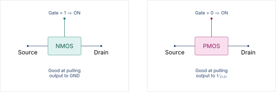
Two flavors of MOSFET exist. An NMOS transistor conducts when the gate voltage is high (logic 1). A PMOS transistor conducts when the gate voltage is low (logic 0). The asymmetry is deliberate. NMOS transistors are good at pulling the output down to ground (logic 0) but poor at pulling it up to the supply voltage. PMOS transistors are good at pulling the output up to the supply voltage (logic 1) but poor at pulling it down. Pairing them gives a circuit that drives the output cleanly in both directions.
The CMOS inverter
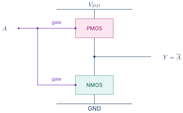
The simplest complete CMOS gate is the inverter: one PMOS transistor between the supply voltage and the output, and one NMOS transistor between the output and ground. Both gates are tied to the same input signal .
When : the PMOS transistor turns on (gate is low), connecting the output to . The NMOS transistor turns off (gate is low), disconnecting the output from ground. The output is pulled to , which represents logic 1. The gate computes .
When : the PMOS turns off and the NMOS turns on. The output is pulled to ground, logic 0. The gate computes .
In neither case do both transistors conduct simultaneously (ignoring the brief overlap during the input transition). This means no static current flows from to ground through the inverter in steady state. The only current flows during the switching transient, when the output capacitance is being charged or discharged. This property is the reason CMOS technology dominates digital electronics: it burns energy only when switching, not when sitting idle.
CMOS NAND and NOR
The CMOS construction rule generalizes to any logic function. A CMOS NAND gate with two inputs and uses two PMOS transistors in parallel between and the output, and two NMOS transistors in series between the output and ground.
Parallel PMOS (pull-up network): The output is pulled high whenever or , because either PMOS path connects to the output. This is the OR of the complemented inputs.
Series NMOS (pull-down network): The output is pulled low only when and , because both NMOS transistors must conduct to complete the path from the output to ground. This is the AND of the true inputs.
The result is , the NAND function. The NOR gate swaps the topology: PMOS in series (output high only when both inputs are low) and NMOS in parallel (output low when any input is high), giving .
Why NAND and NOR are preferred
Chapter 4 showed that NAND and NOR are each universal gates. In CMOS technology they have a second advantage: they are the simplest gates. A two-input NAND uses four transistors (two PMOS, two NMOS). A two-input AND would need six: the four transistors of a NAND plus the two transistors of an inverter on the output. Every additional stage of logic adds delay. For this reason, real standard-cell libraries are dominated by NAND, NOR, and inverter cells, along with compound gates (AOI, OAI) that fold an AND-OR or OR-AND function and its inversion into a single pull-up/pull-down stack.
02.From Transistors to Gates to Netlists
A chip designer never draws individual transistors for a million-gate design. Instead, a library of pre-characterized standard cells provides a catalog of gates: inverters, NAND2, NAND3, NOR2, NOR3, AOI21, OAI22, multiplexers, flip-flops, buffers, and dozens of other common functions. Each cell has a fixed height (so rows of cells tile neatly across the chip) and a variable width proportional to the number of transistors inside.
A gate-level netlist is a list of standard-cell instances and the wires that connect them. It is the output of logic synthesis, the process that reads a hardware description in a language like Verilog or Chisel (Chapter 10) and maps it to the available cells in a target library. The netlist is structural: it says “this NAND2 output connects to that NOR3 input” without specifying where on the chip the cells will physically sit. Placement and routing, a later step in the physical design flow, assigns coordinates and metal traces.

The netlist is important to the computer architect because it is where the abstract world of Boolean functions meets the concrete world of transistors and wires. Every architectural optimization that reduces the number of gates on the critical path, or that replaces a slow gate (high fan-in NOR) with a faster topology (tree of NAND2 gates), directly reduces the cycle time or the area of the chip.
Fan-in and its effect on delay
The fan-in of a gate is the number of inputs it accepts. A 2-input NAND has fan-in 2. A 4-input NOR has fan-in 4.
Fan-in affects delay because of the pull-down (or pull-up) stack. In a NAND gate, the NMOS transistors sit in series. Each additional input adds one more transistor to the series chain. A longer series chain has a higher total on-resistance, which slows the discharge of the output capacitance. A 4-input NAND is roughly twice as slow as a 2-input NAND, not because the logic is more complex, but because four NMOS transistors in series have four times the resistance of one (and the output capacitance also grows).
In a NOR gate, the PMOS transistors sit in series. Because PMOS transistors are inherently slower than NMOS transistors of the same size (hole mobility is about 2 to 3 times lower than electron mobility in silicon), high-fan-in NOR gates are particularly slow. This physical asymmetry is why NAND-based logic is faster than NOR-based logic in CMOS, and why synthesis tools prefer NAND over NOR when both are functionally equivalent.
Fan-out and loading
The fan-out of a gate is the number of gate inputs it drives. Every gate input presents a small capacitive load to its driver. When a gate drives many inputs, the total load capacitance grows, and the driver must push more charge through its transistors to swing the output voltage. The result is a longer transition time and a larger propagation delay.
Think of a single fire hose (the driver) connected to multiple sprinkler heads (the fan-out). Each sprinkler head needs water pressure (charge). The more heads connected, the longer it takes for the hose to bring all of them up to full pressure.
When the fan-out grows beyond four or five, the standard remedy is to insert a buffer (which is just two inverters in series, so logically transparent) between the driver and the fan-out tree. The buffer has larger transistors that can source more current, reducing the delay penalty. Automatic buffer insertion is a standard step in physical design.
03.Propagation Delay
The propagation delay of a gate, , is the time between the input change and the corresponding output change, measured at the 50% voltage crossing points. Every gate in a standard-cell library is characterized with values for each input-to-output arc, measured across a range of input slew rates and output load capacitances.
A first-order model of gate delay uses the RC time constant. The gate’s transistors act as a resistance (when on), and the output node has a total capacitance that includes the drain diffusion capacitance of the gate’s own transistors, the wire capacitance, and the input capacitances of all gates being driven. The time to charge or discharge through is proportional to :
The factor 0.69 comes from , since the 50% voltage crossing for an RC circuit occurs at .
Path delay and the critical path revisited
The delay through a combinational circuit is the sum of the gate delays along the longest path from any input to any output. Chapter 6 called this the critical path, and the setup constraint determines the maximum clock frequency.
From the transistor perspective, reducing the critical-path delay means either reducing the number of gate stages (logic depth), reducing the fan-in of the gates on the path (shorter transistor stacks), reducing the fan-out each gate must drive (less capacitance), or using faster transistors (a more advanced process node). The architect rarely touches transistor sizes directly, but every architectural choice that increases or decreases the logic depth of the critical path has a direct impact on the clock frequency.
Contamination delay
The contamination delay is the shortest time from an input change to the first movement of the output. It is always less than or equal to . The contamination delay matters for hold-time analysis: the hold constraint requires that data at the capturing flip-flop not change too soon after the clock edge, and the fastest path through the combinational logic determines whether that constraint is met.
For timing sign-off, the design tool computes both worst-case (slow corner, high temperature, low voltage) delays for setup analysis and best-case (fast corner, low temperature, high voltage) delays for hold analysis. A design that passes both checks across all process, voltage, and temperature (PVT) corners is said to have timing closure.
04.Technology Scaling and Moore’s Law
In 1965, Gordon Moore observed that the number of transistors on a chip was doubling roughly every year [1]. He later revised the period to about two years. This empirical trend, known as Moore’s law, is not a physical law but an economic observation about the pace at which the semiconductor industry has been able to shrink transistor dimensions and increase chip density.
A technology node labels one generation of the manufacturing process. The name originally referred to the smallest feature that the lithography system could print. A 1 μm (micrometer) process in 1985 could print features 1 μm wide. A 180 nm process in 1999 could print features 0.18 μm wide. Below 22 nm, the node name became a marketing label rather than a physical measurement. Intel’s “Intel 7” node, TSMC’s “N5” node, and Samsung’s “5 nm” node all refer to different physical dimensions despite sharing a similar-sounding label.
Dennard scaling
In 1974, Robert Dennard and colleagues showed that when transistor dimensions shrink by a factor , the voltage and current scale down by the same factor, keeping the power density (watts per square centimeter) roughly constant [2]. Under ideal Dennard scaling:
Table 1. Dennard scaling relationships when dimensions shrink by a factor .
| Parameter | Scaling factor |
|---|---|
| Feature size | |
| Supply voltage | |
| Current | |
| Capacitance | |
| Frequency | (faster) |
| Transistor count | |
| Power per transistor | |
| Power density | (constant) |
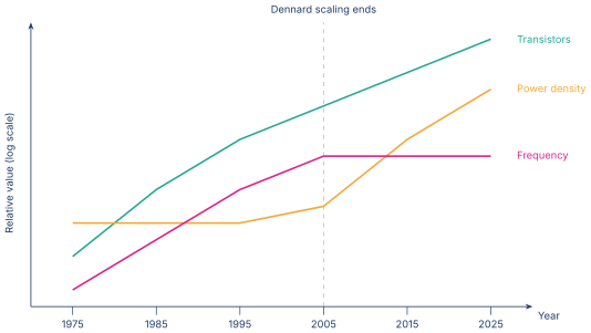
Dennard scaling was the engine behind the era of free performance improvement from the mid-1970s through the early 2000s. Each new technology node delivered more transistors, higher clock frequencies, and roughly constant power density. Programmers benefited automatically: existing software ran faster on the next generation of hardware without any changes.
The end of Dennard scaling
Around 2005, at the 90 nm and 65 nm nodes, Dennard scaling broke down. The supply voltage could no longer shrink proportionally because the transistor threshold voltage (, the minimum gate voltage needed to turn the transistor on) was approaching a floor set by subthreshold leakage. Reducing further would allow too much current to leak through transistors that are supposed to be off.
With stuck near 0.7 to 1.0 V, shrinking transistors still packed more of them onto a chip (Moore’s law continued), but the power density began to rise instead of staying constant. Clock frequencies hit a ceiling around 4 GHz in mainstream designs. The industry responded by shifting from faster single cores to more cores at moderate frequencies [3], a transition often described as the end of the free lunch for programmers. Multicore architectures lie beyond this book.
05.Power Consumption in CMOS
Total power in a CMOS circuit has two components: dynamic power and static power (also called leakage power).
Dynamic power
Dynamic power arises from the charging and discharging of capacitances each time a gate switches. The energy to charge a capacitor to voltage is . The same energy is dissipated during discharge. For a gate that switches at frequency with an activity factor (the fraction of clock cycles in which the gate actually toggles):
The dynamic power equation shows why voltage scaling is so effective. Power is proportional to . Reducing the supply voltage by 10% reduces dynamic power by roughly 19%. This quadratic dependence drives the voltage-frequency scaling techniques (DVFS) used in every modern processor and mobile SoC.
Static (leakage) power
Even when no gates are switching, transistors leak current. The dominant leakage mechanism in modern processes is subthreshold leakage: a small current flows between source and drain even when the gate voltage is below the threshold. As transistors shrink and decreases, subthreshold leakage increases exponentially.
Static power is simply:
where is the total leakage current summed across all transistors on the chip. At the 7 nm and 5 nm nodes, leakage can account for 30 to 50 percent of the total chip power. Managing leakage is a first-order concern for battery-powered devices.
Table 2. Techniques for reducing leakage power.
| Technique | Description |
|---|---|
| Power gating | Switch off to idle blocks using a header or footer sleep transistor. Eliminates both dynamic and leakage power for the gated block at the cost of a wake-up latency. |
| Multi- | Use high- transistors on non-critical paths (low leakage, slower) and low- transistors on the critical path (higher leakage, faster). |
| Body biasing | Apply a reverse bias to the transistor body to raise and reduce leakage during idle periods. |
| Voltage scaling | Reduce during low-activity periods. Helps both dynamic and leakage power. |
06.The PPA Tradeoff
Every design decision at every level of abstraction, from the transistor sizing of a single gate to the number of execution units in a superscalar processor, ultimately lands on a three-way balance among performance, power, and area. The PPA tradeoff is the central economic reality of chip design.
Performance means speed: the maximum clock frequency multiplied by the work done per clock cycle. Faster transistors (lower , shorter gate length) improve frequency but increase leakage. Wider datapaths and deeper pipelines increase the work per cycle but consume more area and power.
Power means energy per unit time. Lower power enables longer battery life, cheaper packaging (fewer pins for power delivery, simpler heat sinks), and higher-density rack deployments in datacenters. The dynamic and static power equations above show the knobs available: voltage, frequency, capacitance (area), and threshold voltage.
Area means the number of square millimeters of silicon consumed. A smaller chip fits more dies per wafer, reducing cost per unit. A larger chip has more room for cache, more execution units, and more I/O, but the manufacturing yield (fraction of working dies) drops sharply as die area increases because a single defect kills the entire die.
Wire delay and the interconnect wall
As transistors shrink, gates get faster, but wires do not automatically get faster. The resistance of a wire increases as its cross-sectional area decreases, and the capacitance per unit length stays roughly constant or even increases because neighboring wires move closer together. At the 90 nm node and below, wire delay began to rival or exceed gate delay on long global routes.
This trend, sometimes called the interconnect wall, pushed designers toward architectural solutions: keeping data local (caches, register files, near-memory compute), tiling the chip into physically small processing elements that communicate over short wires, and using repeater buffers on long signals. The memory hierarchy of Part IV, tiled multicore layouts, and chiplet architectures are all responses to the physics of wires.
Modern process innovations
The industry has introduced several process-level innovations to continue the Moore’s-law trajectory despite the end of Dennard scaling:
FinFET (2012, 22 nm). Instead of a flat transistor channel on the silicon surface, the channel is shaped into a thin vertical fin wrapped by the gate on three sides. The greater gate control reduces leakage and improves switching speed. Intel introduced FinFET at 22 nm. TSMC and Samsung followed at 16/14 nm.
Gate-All-Around (GAA, 2022, 3 nm). The next step beyond FinFET. The channel is a stack of horizontal nanosheets completely surrounded by the gate material. Samsung’s 3 nm GAA process was the first in production. Intel’s equivalent (RibbonFET) appears at their Intel 20A node.
Extreme Ultraviolet (EUV) Lithography. Uses 13.5 nm wavelength light (compared to 193 nm for prior deep-UV lithography) to print finer features in fewer mask exposures. EUV became production-ready at the 7 nm and 5 nm nodes and is essential for 3 nm and below.
Backside Power Delivery (BSPDN). Routes the power supply rails through the back of the wafer rather than through the front-side metal stack where signal wires live. This frees up routing tracks on the front side, reduces IR drop, and allows denser standard-cell placement. Intel’s Intel 20A and TSMC’s N2 both adopt backside power delivery.
07.Connecting to the Rest of the Book
This chapter has descended from the gate-level abstractions of Chapters 4 through 6 to the transistor physics that make those gates real. The key takeaways for every subsequent chapter are:
Gate delay grows with fan-in (series transistor stacks) and fan-out (capacitive loading). Critical-path delay determines the maximum clock frequency, and architectural decisions that change the logic depth of the critical path change the frequency directly.
Power splits into dynamic () and static (), and both scale with the transistor technology. The end of Dennard scaling is the reason modern processors invest in parallelism (wider pipelines, more cores, vector units, accelerators) rather than simply raising the clock.
The PPA tradeoff is inescapable. Every architectural feature added to a design has a cost in silicon area and power that must be justified by the performance it delivers for the target workload.
Chapter 10 introduces the languages (Verilog, SystemVerilog, VHDL, Chisel) that express digital designs at the register-transfer level, one layer above the netlist. The project chapter that follows (Chapter 11) uses Chisel to build a 32-bit ALU whose gate-level netlist is the direct descendant of the transistor-to-gate story told here.
08.Worked Examples
09.Exercises
References
- [1]Moore, Gordon E. (1965). “Cramming More Components onto Integrated Circuits.” Electronics, 38(8), pp. 114--117.
- [2]Dennard, Robert H. and Gaensslen, Fritz H. and Yu, Hwa-Nien and Rideout, V. Leo and Bassous, Ernest and LeBlanc, Andre R. (1974). “Design of Ion-Implanted MOSFETs.” IEEE Journal of Solid-State Circuits, 9(5), pp. 256--268. doi:10.1109/JSSC.1974.1050511
- [3]Hennessy, John L. and Patterson, David A. (2019). “Computer Architecture: A Quantitative Approach.” Morgan Kaufmann.