The Computing Stack
September 13, 202661 min readbeginner
Computer architecture is the study of how the hardware that runs software is organized. This opening chapter introduces the field and the vocabulary the rest of the book uses. The discussion moves from purpose…
Computer architecture is the study of how the hardware that runs software is organized. This opening chapter introduces the field and the vocabulary the rest of the book uses. The discussion moves from purpose to history to structure. The middle of the chapter develops the conceptual machinery later chapters depend on, including the distinction between architecture, microarchitecture, and organization, the layers of abstraction that connect transistors to applications, the stored-program idea that remains the deepest design choice in the field, and a side-by-side preview of the four instruction-set families that thread through every subsequent chapter.
01.The Purpose of Computation
Every computation answers a question. A spreadsheet sums a column of payroll figures. A navigation app turns the question how do I get there into a sequence of left and right turns. A radiology workstation reads a chest scan and tells the doctor where to look. A weather model predicts tomorrow’s rainfall across a city block. A trained language model produces the next word in a sentence. Behind each of these tasks sits a machine that takes inputs, applies a fixed set of operations, and produces outputs. That machine is the computer, and the design of that machine is the subject of this book.
The questions that computers answer have changed enormously over the past eighty years, but the shape of the underlying activity has not. A computation is a finite sequence of well-defined steps that transforms data. Each step is small enough that a machine can carry it out without ambiguity. The sequence is long enough that the result is genuinely useful. A circuit that adds two thirty-two-bit numbers completes one such step in well under a nanosecond. A modern processor running a video game performs more than a hundred billion such steps every second. The hardware that gets us from a single addition to a hundred billion per second is what we mean by a computer.
It helps to separate two ideas that are often blurred. Computation is the abstract activity of transforming data. Computing is the practical business of building, programming, and using machines that perform computations at speeds and scales useful in the real world. The first idea is older than electricity. Mathematicians worked out the rules of arithmetic, of finite-step procedures called algorithms, and of logical inference long before any switch was thrown. The second idea is what built the modern world. Computer architecture sits between the two. It studies how to organize circuits so that they faithfully realize the abstract activity we want them to perform.
The reason to build a computer at all is therefore practical. A computer is a tool for outsourcing finite sequences of well-defined steps to a machine that performs them faster, more reliably, and at lower cost than a person ever could. The reason to study the design of a computer is structural. The same handful of architectural ideas, applied at different scales, explains almost every modern machine. The caching strategy that gives a personal phone its responsiveness gives a datacenter its throughput. The pipelining trick that speeds up an embedded controller in a coffee maker speeds up the fastest processors in a supercomputer. The structural ideas are the subject of the rest of the book.
02.Reasons to Study Computer Architecture
The most direct reason to study computer architecture is that anyone who writes software lives with the consequences of architectural decisions. A web application that runs three times slower than the competitor is rarely improved by a faster network or a larger budget. It is improved by code that uses the cache better, by a database that respects the disk’s access pattern, and by a runtime that does not stall waiting for memory. The mechanisms that make those improvements possible are decided at the architectural level. A programmer who does not see them works around them by guesswork. A programmer who does see them works with them, and the difference shows up in profiling.
The discipline rewards different kinds of readers for different reasons. A compiler writer needs to know which instruction selections expose the most internal parallelism on a given processor. An operating system developer needs to know how the memory management unit behaves across the privilege boundary so the kernel can hand pages back and forth without losing safety. A security researcher needs to know what timing channels the cache leaves behind. A hardware designer needs to know every assumption the software stack makes about ordering, alignment, and atomicity, because the next chip cannot afford to break those assumptions silently. Each of these readers takes away a different subset of the same architectural vocabulary. The vocabulary itself is shared.
There is also a softer reason. Computer architecture is one of the few engineering disciplines in which an undergraduate can build a working artifact, from logic gates up through an instruction set, in a single semester. The exercise produces a kind of understanding that no amount of high-level reading delivers. The reader has to commit to specific bit-width choices, decide where the program counter lives, write the code that decodes an instruction into control signals, and watch the design run a program. The book’s project chapters return to this exercise repeatedly. Each one builds a small but complete piece of hardware that the reader can simulate and inspect, so that abstract ideas like the fetch stage and the load-store queue have concrete referents.
A more forward-looking reason is that the field is still in motion. The end of Dennard scaling and the slowing of Moore’s law have made the past fifteen years the most architecturally productive era since the 1970s. Modern processors have learned to do dozens of instructions in flight at once. The memory hierarchy has grown its third level on-die, then absorbed parts of main memory through CXL. Domain-specific accelerators have moved from research papers to consumer phones. Confidential computing has put hardware enclaves into datacenter servers. None of these developments are settled, and the ones that are not yet built are the subject of current conference proceedings. A reader who finishes this book is positioned to follow that literature and, at the graduate or PhD level, to contribute to it.
03.A Brief History of Computing
The history of computing is told here in four short passes, each covering roughly half a century. The aim is not exhaustive coverage but a sense of how the modern computer’s shape emerged from a sequence of ideas, each of which solved a problem the previous one had created.
Mechanical calculators to the analytical engine
The desire to mechanize calculation is much older than electricity. The Pascaline of 1642, built by the nineteen-year-old Blaise Pascal to help his father add tax receipts, performed addition and subtraction through a chain of geared wheels. Gottfried Leibniz extended the idea in 1672 with the stepped reckoner, which could multiply and divide. These machines were arithmetic instruments rather than computers in the modern sense. They executed exactly one fixed procedure, and the operator selected the inputs by turning dials.
The conceptual shift that made the modern computer possible came from Charles Babbage. His Difference Engine of 1822 was a mechanical device for tabulating polynomial values, and his Analytical Engine, designed but never completed in his lifetime, was a general-purpose programmable machine that drew its operations from a sequence of punched cards. The card idea was borrowed from the Jacquard loom, which had used punched cards since 1801 to control the weave pattern of silk fabric. Ada Lovelace’s 1843 notes on the Analytical Engine include an algorithm for computing Bernoulli numbers and a recognition that the machine could in principle manipulate symbols, not only numbers. Lovelace’s notes are usually cited as the first published computer program.
The other thread that connects this era to the modern field is George Boole’s 1854 An Investigation of the Laws of Thought [1], which formalized logical reasoning as algebra over the values true and false. Boolean algebra would later become the mathematical foundation on which every digital circuit is designed. The closing event of the mechanical era is Herman Hollerith’s tabulating machines, used to process the 1890 United States census. The company Hollerith founded eventually became IBM. The path from punched-card tabulators to electronic computers runs through that company.
ENIAC, EDVAC, and the von Neumann report
The first electronic computer was the Electronic Numerical Integrator and Computer, ENIAC, built at the University of Pennsylvania and completed in 1945. It contained roughly eighteen thousand vacuum tubes, weighed thirty tons, and computed roughly one thousand times faster than any electromechanical predecessor. ENIAC was electronic but not yet a stored-program machine. Programming it meant physically rewiring the patch panels for each new task, which could take weeks. The internal state of the program was not in memory but in the wires themselves.
The decisive idea of the era was articulated in 1945 by John von Neumann in his draft report on the proposed successor machine, EDVAC [2]. The report described a single addressable memory that held both the instructions and the data of a program, a central control unit that fetched and executed instructions from that memory in sequence, and an arithmetic unit that performed the operations the instructions specified. The design was not solely von Neumann’s. The original team also included J. Presper Eckert, John Mauchly, and other engineers, but the report carried his name and the name stuck. To this day, the term von Neumann architecture refers to a stored-program machine with one unified memory for code and data.
The first stored-program computer actually to run a program was the Manchester Baby in June 1948, followed by the Cambridge EDSAC in 1949. ENIAC’s successor EDVAC began operation in 1951. By the mid-1950s the stored-program design was universal. Programs could now be loaded as data, computed by the computer itself, and modified at runtime. The implications were immediate. A computer could simulate another computer simply by interpreting its instruction encoding, which is the foundation of every emulator, every virtual machine, and every just-in-time compiler in the modern stack.
From mainframes to microprocessors
The decade after EDVAC saw computers leave the laboratory and enter business and government. The vacuum tube gave way to the transistor, invented at Bell Labs in 1947, which was smaller, cooler, and far more reliable. The transistor enabled the second-generation mainframes of the late 1950s. The integrated circuit, introduced by Texas Instruments and Fairchild in 1958, packed multiple transistors onto a single silicon die and made the third-generation machines of the 1960s possible.
The defining machine of the mainframe era was the IBM System/360, announced in 1964 [3]. It was the first attempt to ship one instruction-set architecture across a range of compatible models at different price and performance points. A customer could buy a small System/360 for departmental work and a large one for the central computing center, and the same program would run on both. The ISA as a stable contract between hardware generations dates from this design. Every modern processor family that promises forward and backward compatibility, including x86-64 and ARM AArch64, descends conceptually from the System/360.
The size of computers fell sharply during the 1970s. Digital Equipment Corporation’s PDP minicomputers brought interactive timesharing to universities and research labs at a tenth the size and cost of a mainframe. The arrival of the microprocessor in 1971 was the next compression. Intel’s 4004, originally designed for a Japanese calculator company, packed an entire 4-bit central processor onto a single chip. The 8-bit 8080 from Intel in 1974, the 6800 from Motorola in the same year, and the Z80 from Zilog in 1976 followed. By the late 1970s these chips were inexpensive enough that engineers could build a complete usable computer around one of them, which is what created the personal computer industry. The IBM Personal Computer of 1981 paired an Intel 8088 with a small amount of memory and a floppy disk drive, and the chain of architectural decisions that followed that pairing still shapes the desktop and server market.
The 1980s brought the reduced-instruction-set computer movement, which argued that a smaller, more uniform instruction set could be implemented at a higher clock rate and was easier for compilers to target. The MIPS architecture from Stanford and the SPARC architecture from Sun Microsystems pursued this idea commercially, and the Berkeley RISC project laid the academic foundation. ARM belongs to the same lineage. It began at Acorn Computers in Cambridge, produced its first silicon in 1985, and reached a shipping product in the 1987 Acorn Archimedes. The RISC and CISC debate eventually softened into convergence. Modern Intel and AMD x86-64 chips decode their variable-length CISC instructions into a stream of RISC-like internal operations executed by a deeply pipelined out-of-order core. Modern ARM and RISC-V chips have added many of the optimizations that were once thought to be CISC features. The two camps have met in the middle.
From single-core to multicore to heterogeneous
The 1990s and early 2000s were dominated by the steady increase of processor clock frequency. From 1986 to 2003, single-thread performance roughly doubled every two years, fueled by smaller transistors and deeper pipelines. The Intel Pentium 4 Prescott core of 2004 reached 3.8 GHz on a thirty-one-stage pipeline. It was the high point of that trajectory and the beginning of its end. The next geometry shrink no longer reduced the per-transistor power proportionally, so further frequency scaling would have melted the chip. The industry responded by replicating the processor on the same die rather than speeding it up. Multicore had been a research idea for a decade. It became a product reality in 2005 with the dual-core Intel Pentium D and the dual-core AMD Athlon 64 X2. A general- purpose CPU has had more than one core ever since.
The second great shift was mobile. Apple announced the iPhone in 2007 and the smartphone became the dominant computing device of the next decade. The chip inside it was an ARM, not an x86. ARM’s low-power, license-the-design business model fit the mobile market exactly. By 2015, ARM cores outnumbered every other ISA family combined, including x86. The same era saw graphics processors become programmable for general-purpose work. NVIDIA released the first CUDA toolkit in 2007, OpenCL followed in 2008, and within a decade GPUs were the standard engine for scientific computing and, by 2015, for machine learning.
The third shift is the one still underway. The slowing of Moore’s law and the end of Dennard scaling have made general-purpose performance gains harder to come by, and the industry has responded by adding domain-specific accelerators for the work that benefits most [4]. Google announced its first Tensor Processing Unit in 2016. Apple shipped a custom Neural Engine on every iPhone from 2017 onward. The 2020 Apple M1 was the first widely used desktop processor built around an ARM core with custom co-processors for graphics, neural inference, and video. AMD, Intel, NVIDIA, and others have followed similar paths. Confidential computing, chiplet packaging, near-data processing, and persistent memory are at various stages of moving from research papers into commercial products.
RISC-V, the open-source ISA designed at Berkeley starting in 2010, is the architectural answer to a different question. It asks whether the foundational contract between hardware and software needs to be controlled by any single vendor. As of 2026, RISC-V has shipped in billions of microcontrollers, has entered the application-processor market for low-power devices, and is the target of an active research community that prototypes new ideas on open-source RISC-V cores like BOOM, Rocket, and CVA6 before they reach commercial silicon. The book uses RISC-V as the running example precisely because the full architecture is publicly documented.
04.Analog and Digital Computers
The computers in this book are without exception digital. They work by representing every quantity as a binary number, encoded in switches that are either on or off. The choice to build computers this way was not obvious in the 1940s. A meaningful tradition of analog computation ran in parallel with the early electronic computers and for a time looked competitive.
An analog computer represents quantities by continuous physical signals such as voltage, current, fluid pressure, or mechanical displacement. An operational amplifier configured as an integrator takes an input voltage and produces an output voltage whose value is the running integral of the input over time. Wire a few of these together and they solve differential equations in real time. Analog computers were used to design aircraft wings, train naval gunners, and model nuclear reactors well into the 1970s. They were fast at the problems they were good at, often using nothing more than a handful of components, and they could be very precise within their measurement range.
The reason digital displaced analog is not that digital is fundamentally faster. It is that digital is exactly reproducible. A bit either is or is not set. There is no drift, no calibration, no tolerance, no integration error that accumulates with each operation. A digital computer running the same program on the same input today produces exactly the same output it would have produced yesterday, on the next machine, on the next continent. An analog computer’s output depends on the exact temperature of the room, the age of its capacitors, and the precision of its voltage references. Adding two analog quantities is a noisy operation that loses a little fidelity each time. Adding two digital numbers is exact.
The other quality digital has and analog does not is general purposeness. A digital computer programmed to multiply matrices today can be reprogrammed to render a video frame tomorrow with no hardware changes. Analog computers were not programmable in this sense. The program was the wiring. By the late 1970s the speed advantage of analog computation was gone for almost every problem of practical interest, and the field shrank into a niche occupied today by a small number of specialized signal-processing devices. The book treats only digital computers from this point forward.
05.Hardware, Software, and Firmware
Three terms cover almost every distinct piece of a computer system. Hardware is the physical apparatus. The silicon chips, the printed circuit boards, the wires, the heatsinks, the screen, and the keyboard are all hardware. Hardware is what the manufacturer ships in the box. Software is the body of instructions and data that runs on top of the hardware. The operating system, the compiler, the web browser, the spreadsheet, and the program the user wrote yesterday are all software. Software is what changes most. New software arrives every day. New hardware arrives every few years. Firmware is the third category. It is software, in the sense that it consists of instructions stored in memory and executed by a processor, but it is software that is tightly tied to a specific piece of hardware and that the user is not expected to change. The boot code in the BIOS or UEFI of a personal computer is firmware. So is the embedded controller code in a hard drive, a graphics card, a network card, and the small auxiliary processors found throughout any modern system.
The boundary between hardware and software is the most important one in this book. Where it falls is partly a matter of physical necessity. A NAND gate has to exist as actual silicon. There is no way to write a program that creates a new logic gate. The boundary is also partly a matter of design choice. A floating-point multiplication can be implemented as a dedicated circuit in the processor, in which case it takes a few clock cycles and feels like hardware to the programmer. The same operation can be implemented instead as a sequence of integer instructions in software, in which case it takes hundreds of cycles and feels like a library function. The same operation has been on both sides of the line at different points in computing history. Early personal computers without floating-point hardware emulated it in software. Modern processors implement it in hardware. Many specialized accelerators move it back into hardware in a different form.
Firmware exists because some software is too tightly coupled to the specific hardware to live above the operating system. A network card’s firmware decides how to interpret the bytes coming off the wire. A solid-state drive’s firmware decides which physical flash blocks to write to, when to garbage-collect, and how to handle the wear-leveling. Neither of these decisions is something the operating system wants to make on every operation, and the manufacturer ships them as firmware so the device can present a clean interface to the rest of the system. Firmware is updateable in modern devices but the update process is slow, infrequent, and treated as a serious event. A bricked firmware update can render the device permanently unusable.
The book uses the hardware, software, and firmware split throughout. When a chapter says the processor does something in hardware, the operation is implemented by a fixed circuit. When it says the operating system does something in software, the operation is a program that runs on the same processor that runs every other program. When it says the network card firmware does something, the operation is a program running on a small dedicated processor inside the network card, distinct from the main CPU.
06.The Journey of a Single Instruction
Earlier sections argued at the level of definitions. This section makes the argument concrete by tracing a single computation from its source code to its execution on hardware. The example is the smallest function worth writing.
A C program that adds two numbers
The listing below shows the source program. It takes two integer arguments, computes their sum, and returns the result. There is no control flow, no memory access, no library call, no floating-point arithmetic. The whole behavior of the function fits on two lines of code.
The smallest useful C function, used as the running example throughout this section.
| int sum2(int a, int b) { | |
| return a + b; | |
| } |
Despite the modesty of the source code, the work that runs when sum2 is called is not nothing. The arguments a and b arrive in specific places mandated by the platform’s calling convention. The hardware adds them using a specific instruction encoding. The result leaves in another specific place that the caller knows to look at. The three pieces are argument passing, the arithmetic itself, and return-value passing. Each of these is a choice made by the instruction set architecture, and the choices differ across machines.
The compiled assembly we will read
The same source compiled with optimization gives different assembly under each of the four instruction-set families this book treats throughout, which produce three distinct listings because Intel and AMD implement the same x86-64 ISA. The listing below is the RISC-V translation, the listing below the ARM A64 translation, and the listing below the x86-64 translation. The compiler used is GCC at the -O2 optimization level. The output below is what GCC actually emits on each platform, lightly trimmed of directives that the book does not yet need.
The function sum2 compiled to RISC-V RV64I assembly.
| sum2: | |
| addw a0, a0, a1 | |
| ret |
The function sum2 compiled to ARM A64 assembly.
| sum2: | |
| add w0, w0, w1 | |
| ret |
The function sum2 compiled to x86-64 assembly in AT&T syntax.
| sum2: | |
| leal (%rdi,%rsi), %eax | |
| ret |
Each version is two instructions. The shared structure is striking. On every machine the function does exactly one arithmetic operation and one return. The differences are in where the arguments arrive, which register holds the result, and how the addition is spelled. The RISC-V calling convention puts the first two integer arguments in registers a0 and a1 and uses a0 for the return value, so the ADD reuses a0 as both a source and the destination. The ARM A64 convention is structurally the same, but the registers are named w0 and w1 (for the 32-bit views of x0 and x1). The x86-64 System V convention used on Linux and macOS puts the first two integer arguments in rdi and rsi, expects the return value in rax, and uses the load-effective-address instruction lea rather than an explicit ADD because lea folds an addition into a single micro-op without disturbing the processor’s flag register.
What the processor does, step by step
Consider the RISC-V version, since it has the simplest encoding. When the function sum2 is called, the processor’s program counter holds the address of the first instruction. What follows is one trip through the fetch-decode-execute cycle for each of the two instructions.
For the addw a0, a0, a1 instruction:
-
Fetch. The processor reads the four bytes at the address in the program counter. RV64I instructions are always four bytes long, so the fetch is one aligned memory read. The optional C extension adds sixteen-bit encodings, which a later section in this chapter introduces.
-
Decode. The hardware breaks the four-byte instruction into its fields. The opcode field identifies this as a 32-bit register-to-register arithmetic operation. The three register fields name
a0as the destination anda0anda1as the two sources. The function-code fields select the ADD operation specifically. -
Read operands. The processor reads the values from registers
a0anda1out of the register file. -
Execute. The arithmetic logic unit adds the two 32-bit values.
-
Write back. The 32-bit result is written to register
a0. -
Advance the program counter. The processor adds four to the program counter so it points to the next instruction.
For the ret instruction:
-
Fetch. The four bytes at the new program counter are read from memory.
-
Decode. The hardware recognizes
retas a pseudo-instruction for an indirect jump. The instruction names registerra, the architectural return-address register, as the source of the target address. -
Read operand. The processor reads the value of register
ra. -
Execute. The new program counter is computed by taking the value of
raas is. -
Write back. The program counter is updated to the new value.
The function has now returned. The caller’s address is in the program counter, the return value is in register a0, and the registers and memory the function had access to are in the state the caller expects.
The questions this raises
A function as short as sum2 already implies a number of deeper questions, each of which a later chapter answers in detail.
How did the compiler know to put the first argument in a0 and the second in a1? That is the calling convention specified by the RISC-V ABI. Part II of the book covers the calling conventions for all four ISA families.
How did the processor decode the bit pattern into a control signal pattern in a single clock cycle? That is the work of the decoder circuit. Part III draws the complete single-cycle datapath, including the decoder.
What happened during fetch, when the processor had to wait for memory to deliver the instruction? Did it really wait? Modern processors do not. They use caches, branch predictors, and out-of-order execution to keep the pipeline full while memory is slow. Part IV covers caches and Part V covers the techniques that keep work flowing despite memory latency.
What if the program had been encoded in ARM or x86-64 instead of RISC-V? The same arithmetic operation would have used a different encoding, a different register, and a slightly different microarchitecture. The decoder would have done more work for x86 because the instruction is variable-length, and roughly the same amount of work for ARM and for RISC-V, since both use a fixed-width 32-bit encoding with 5-bit register fields. The function would have returned with the same numerical result.
The book returns to each of these questions in detail. The point of this section is that the journey of even a tiny function passes through every layer of the computing stack, and the entire stack is the subject of the rest of the book.
07.Three Views of a Computer
A computer can be examined at three distinct levels of detail, each useful for a different purpose. The names of the three levels are fixed by long practice in the field. They are architecture, microarchitecture, and organization. The boundaries between them are not perfectly sharp, but the distinction is real and is used throughout this book.
Architecture, the contract between hardware and software
The architecture of a computer is the specification of what the machine looks like to a programmer or a compiler. It enumerates the instructions the machine accepts, the registers and memory the instructions can name, the layout of those operands, the rules for sequencing instructions and handling exceptions, and the operations the privileged software can perform. Architecture is the contract that software depends on. Two machines have the same architecture when a program written for one will run on the other without recompilation.
Most of architecture is captured by the instruction set architecture, the ISA. The RISC-V Unprivileged Spec [5], the ARM Architecture Reference Manual [6], the Intel Software Developer’s Manual [7], and the AMD Architecture Programmer’s Manual [8] are each architectural documents in this sense. They describe what each instruction does in terms of the visible register file and memory, what flag bits change, and what exceptions can be raised. They say nothing about how the instructions are actually carried out.
Microarchitecture, the implementation of the contract
The microarchitecture of a computer is everything the architecture leaves unspecified. Two processors with the same architecture can have wildly different microarchitectures. An ARM Cortex-A53 is an in-order, two-issue, eight-stage core. An ARM Cortex-X3 is an out-of-order, six-wide, fifteen-stage core. They run the same ARMv8-A instructions and follow the same architectural contract, but the engineering choices made below the contract are different in every respect.
Microarchitecture includes the depth and width of the pipeline, the cache sizes and replacement policies, the branch predictor design, the number of physical registers used for renaming, the load and store queue capacities, the issue width, the kinds of functional units the core has, and many other choices. The graduate-fundamentals chapters of the book cover microarchitecture in detail, and the four case-study chapters at the end of Part V compare public reference designs from each of the four ISA families side by side.
Organization, the system view
The organization of a computer is the view in which one or more processors, memories, accelerators, and input/output devices compose into a complete machine. A modern server has many cores arranged in a mesh interconnect on one die, multiple dies arranged into a chiplet package, multiple sockets arranged on a motherboard, and many sockets arranged in a rack. Each level of that composition is part of the system’s organization.
Organization choices and microarchitecture choices interact. A larger shared cache on the die changes how each core’s local cache should behave. A larger socket count changes the interconnect protocol. Organization-scale questions of this kind dominate multicore and datacenter-scale design, both of which lie beyond this book.
The place of microcode between architecture and microarchitecture
Microcode sits in an awkward position between the architecture and the microarchitecture. It is a sequence of very small operations executed by the hardware to implement a single architecturally visible instruction. The small operations themselves are not part of the architecture, since software cannot see them or modify them, but they are also not fixed hardware, since they are stored in a memory inside the processor and can be changed by the vendor through a firmware update.
Microcode was invented by Maurice Wilkes in 1951 as a way to implement complex instructions out of simple ones [9]. It was central to the implementation of CISC processors in the 1970s and 1980s, when an instruction such as the x86 LOOP or ENTER could expand into twenty or more micro-operations. Modern processors still use microcode, but selectively. Simple arithmetic instructions on x86-64 are decoded directly into single micro-operations by hard-coded decoders. Complex instructions, instructions that interact with system state, and instructions that have to be patchable from the field still go through a microcode read-only memory. The patchability is one of microcode’s modern values, since vendors can ship a microcode update through firmware rather than recall the chip when a security vulnerability is found in a complex instruction’s behavior.
For the purposes of this book, microcode is treated as part of the microarchitecture. It is hidden from architecturally visible state, lives in the implementation, and can be redesigned without breaking the architectural contract. The exception is when a microcode update changes architecturally visible behavior to fix a bug, in which case the microcode update becomes a de facto change to the architecture itself.
08.Layers of Abstraction
A modern computer cannot be understood in one shot. Between the silicon transistor and the spreadsheet running on the screen sits a tower of abstractions, each one giving the layer above it a simpler and more useful view of what is happening below. This section walks the tower from bottom to top, naming each layer and saying just enough about what it does to give the rest of the book a shared reference. Figure 1 sketches the seven layers as a vertical stack.
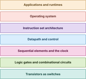
The seven layers are not the only possible decomposition. Some books split the bottom layer into two and merge the top two. The specific count is less important than the underlying observation that each level is a useful place to stop and reason, and each level hides the messy details of the level below.
Transistors as switches
At the bottom of the stack is a single transistor. In a modern processor, this is almost always a metal-oxide-semiconductor field-effect transistor (MOSFET), built on a few cubic nanometers of silicon. A MOSFET has three terminals, the source, the drain, and the gate. Applying a voltage to the gate causes current to flow between source and drain. Removing the voltage stops the current. From the outside, the transistor is an electrically controlled switch.
Modern processors contain tens of billions of these switches. Apple’s M3 Pro shipped in 2023 with around 37 billion transistors on a single die. A high-end NVIDIA GPU shipped the same year with about 80 billion. The book does not work at this level. It treats transistors as the irreducible unit of computation, the way a book on chemistry treats atoms.
Logic gates and combinational circuits
A handful of transistors arranged in a specific way produces a logic gate, a circuit whose output depends only on the immediate values of its inputs. The simplest gate is the inverter, two transistors that output the opposite of whatever voltage is fed in. The next simplest are NAND and NOR, four transistors each, which produce a logical AND or OR with the output inverted. AND, OR, and XOR follow by combining a few NANDs or NORs.
Any boolean function can be built from these gates. Any function, including the ones that compute the next program counter, the result of an addition, the truth of a comparison, and the data flow through a multiplexer. This is the content of Boole’s 1854 algebra, restated in the language of physical circuits. A circuit built entirely of logic gates is called combinational. It has no internal memory, no clock, and its output is a pure function of its current inputs. Part I of the book develops these circuits in detail.
Sequential elements and the clock
A combinational circuit cannot remember anything. To build a computer, the design needs elements that hold state between clock cycles. The fundamental such element is the flip-flop, a small circuit that captures the value of its input on the rising edge of a clock signal and holds that value until the next rising edge. A row of flip-flops with a shared clock is a register. A processor contains hundreds or thousands of registers, used both for the architectural state that the ISA exposes to software and for the many internal buffers and pipelines.
The clock itself is generated by an on-die oscillator at a fixed frequency, often modulated dynamically to save power. Every operation in a synchronous digital circuit happens at a moment defined by the clock. The clock is what gives a computer the property of running at a definite speed.
Datapaths and control
A datapath is the network of registers, multiplexers, ALUs, and memory ports through which data moves inside the processor. The datapath picks operands from the register file, routes them through the ALU, and writes the result back. A control unit is the circuit that decides which datapath operation happens on each cycle. The control unit reads the current instruction (or its decoded form) and produces the signals that steer the multiplexers and enable the ALU function. Part III develops the canonical single-cycle and pipelined datapaths in detail.
The instruction set architecture
The ISA is the contract layer described in a later section. Above it, software exists. Below it, hardware lives. The ISA is the only layer in the stack that is intentionally stable across generations of implementation. Intel’s x86 ISA today still includes instructions Intel shipped in 1978, because programs written against those instructions still run. ARM, RISC-V, and every other modern ISA make similar (if less extreme) backward-compatibility commitments. The visibility of the ISA from software, and its stability across years, is what makes it the load-bearing abstraction of the whole stack.
The operating system and the program loader
Above the ISA sits the operating system. The OS is software in the ordinary sense. It runs on the processor like any other program. But it does work that no ordinary program is allowed to do. It loads other programs into memory, schedules them onto cores, maps and unmaps pages of virtual memory, opens and closes files on the disk, handles network packets arriving from the hardware, and protects each program from every other program. The OS uses privileged instructions, exposed by the privilege-mode features of the ISA, to do this work. Part II returns to the OS interface when it discusses privilege, exceptions, and system instructions.
Applications, runtimes, and language toolchains
At the top of the stack sit the programs that real users actually care about. A spreadsheet is a program. A web browser is a program. A radiology workstation is a program. Each of them was written in a high-level language, compiled or interpreted into the machine code that the processor’s ISA accepts, and loaded into memory by the OS. A language runtime such as the JavaScript engine, the Java Virtual Machine, or the Python interpreter sits between the application and the OS, performing memory management and just-in-time compilation for the application’s own instructions.
The application layer is also where the consequences of every decision made in the layers below are felt. A clever branch-predictor design makes a spreadsheet recalculate faster. A poor cache-replacement policy makes a database query slow. The architectural decisions are far from the user, but their effects are not.
09.The Stored-Program Idea
If a single design choice deserves the label deepest in computer architecture, it is the stored-program idea. The choice is so universally adopted today that calling it a design choice at all feels strange. But in the 1940s it was anything but obvious, and the alternative was actually built first.
Code and data sharing one memory
A stored-program computer places its instructions and its data into the same addressable memory, encoded in the same way as binary numbers, and uses the same load-and-store machinery to retrieve both. To execute the next instruction, the processor fetches it from memory using exactly the mechanism it uses to fetch a data word. This is so familiar to anyone who has touched modern code that the choice can seem trivial. It is not. ENIAC proved that an electronic computer could be built without it. A program ran by physical reconfiguration of the machine’s wires, not by reading from memory. Changing programs took weeks.
The stored-program idea collapses program-loading from weeks to microseconds. It also collapses a more important conceptual boundary. If programs are data, then programs can be written by other programs. Compilers, assemblers, dynamic linkers, virtual machines, and just-in-time engines all rely on this collapse. Every line of code in this book that talks about loading a program, parsing a binary, or generating machine code is taking the stored-program idea for granted.
The fetch-decode-execute cycle
The mechanism by which a stored-program computer actually runs is the fetch-decode-execute cycle, shown in Figure 2. The processor fetches an instruction from the address held in the program counter. It decodes the instruction to determine which operation to perform and which registers or memory locations are involved. It executes the operation, which may read or write data memory and which produces a result. It writes any results back to the register file or to memory. It advances the program counter to point at the next instruction. Then it repeats. The book’s walk through sum2 in a later section was a trace of two trips around this loop.
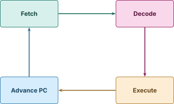
A modern processor executes the cycle billions of times per second per core. The variations across the book come from how those steps are made faster (caches, prediction, prefetching), how they are overlapped with one another (pipelining, out-of-order execution), and how multiple cores execute their own cycles simultaneously (multicore and coherence). The base structure of the cycle, however, has not changed since 1948.
The program counter as another register
The program counter is just a register. It holds an address, like any pointer-typed value in memory. The fetch step reads from that address. The execute step usually adds a small constant to the program counter (four for RISC-V and ARM, the length of the current instruction for x86-64). A branch instruction is just an instruction that updates the program counter to something other than the next sequential address. A function call is a branch that also saves the previous program counter, the return address, so the called function knows where to return.
This view, in which the program counter is just another register, is the lever that makes ordinary processors fast. Predict the branch correctly, and the program counter advances along the correct path without ever stalling the pipeline. Predict it wrong, and the pipeline has to flush the speculative work and start over. The economics of branch prediction is one of the dominant concerns of modern out-of-order microarchitecture. Part V develops branch prediction in detail.
10.Two Memory Organizations: Von Neumann and Harvard
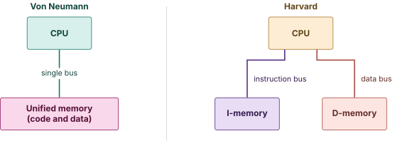
The stored-program idea raises a question. Programs and data both live in memory, but should they live in the same memory? Two canonical answers emerged in the 1940s, and a third hybrid answer dominates modern practice. Figure 3 contrasts the two original organizations side by side.
The von Neumann organization
The von Neumann organization puts instructions and data in a single unified memory, accessed through a single bus. The processor fetches instructions and loads data over the same wires, one at a time. This is the organization described in the EDVAC report, and it has the great virtue of simplicity. A program can grow as large as the memory allows. A self-modifying program can rewrite itself by storing to the address that holds its own code. Most general- purpose computers from the 1950s onward used some form of the von Neumann design.
The cost is contention. If the processor needs an instruction and a data word at the same time, only one of them can come over the bus on any given cycle. This is the von Neumann bottleneck, identified by John Backus in his 1977 Turing Award lecture as the fundamental limit of the architecture [10]. Modern multi-issue processors hit it constantly, which is why almost every modern implementation is some form of modified Harvard rather than strict von Neumann.
The Harvard organization
The Harvard organization, introduced in the 1944 Harvard Mark I, splits instructions and data into two physically separate memories with two separate buses. The processor can fetch an instruction and read or write a data word on the same cycle. The cost is rigidity. The instruction memory and the data memory cannot share space, so a small program with a large data set must work around the allocation, and a self-modifying program cannot work at all because storing to the data memory cannot affect the instruction memory. Pure Harvard designs are now rare outside of embedded microcontrollers, where the rigidity is actually a feature because it prevents stray data from being executed accidentally or by an attacker.
Modified Harvard in modern caches
Almost every general-purpose processor since the late 1980s uses a modified Harvard organization. The main memory is unified von-Neumann-style, with code and data sharing the same physical DRAM. But the level-1 cache nearest the processor is split into a separate instruction cache and data cache that can be accessed in parallel each cycle. The processor sees a Harvard machine at the top of the memory hierarchy and a von Neumann machine below it. The unified main memory keeps software programmable and self-modifying, while the split L1 caches deliver the bandwidth a modern multi-issue core needs. Whether the two caches are kept coherent with each other is an architectural choice rather than a universal property of the organization. On x86-64 the cache hardware does the work, detecting when a store has written to an address whose line is sitting in the instruction cache and invalidating the stale line. On RISC-V and ARM A64 the program has to ask, executing a FENCE.I on RISC-V or an explicit cache-maintenance sequence on ARM A64 after writing instruction bytes, which is why just-in-time compilers emit those instructions before jumping into freshly generated code.
11.Classes of Modern Computers
Computers are not all the same machine at different scales. The constraints that drive design choices vary substantially across classes. A smartphone processor cares about energy per operation above almost everything else. A supercomputer processor cares about throughput on numerical workloads. An embedded processor cares about determinism and unit cost. The architectural techniques central to each class look different as a result. This section enumerates the six classes that the book covers and summarizes the design pressure each one feels. The table below lists the headline parameters side by side.
Table 1. Headline characteristics of the six major classes of modern computers. Power budgets and prices are typical ranges as of 2026.
| Class | Power budget | Price range | Priority |
|---|---|---|---|
| Personal mobile device | 1 to 5 W | $100 to $1500 | Energy |
| Desktop or laptop | 15 to 250 W | $500 to $5000 | Mixed |
| Server or workstation | 100 to 1000 W | $3k to $50k | Throughput |
| Warehouse-scale computer | 5 to 30 MW | $50M and up | Throughput |
| Embedded or IoT | 1 mW to 1 W | $0.10 to $50 | Determinism |
| Supercomputer or HPC | 10 to 100 MW | $100M and up | Throughput |
Personal mobile devices
A personal mobile device, abbreviated PMD by Hennessy and Patterson [11], is what most readers carry in their pocket. A smartphone is the canonical example. Tablets, smartwatches, and augmented-reality headsets fit the same class. The defining constraint is energy per operation. The device runs on a battery that should last a full day under heavy use, and the user expects the screen to respond to input within sixteen milliseconds (the duration of one frame at 60 Hz). The processor inside a 2026-era PMD is typically a heterogeneous SoC with several ARM application cores at different performance tiers, a GPU, a neural processing unit, an image signal processor, an audio DSP, and various other specialized blocks. Most users carry an Apple, Qualcomm, Samsung, or MediaTek SoC. Every one of these is ARM-based, often supplemented by custom co-processors.
Desktops and laptops
The desktop and laptop class includes everything from a Chromebook to a high-end gaming PC. The power budget ranges from 15 watts in a fanless thin laptop to 250 watts in a desktop gaming machine. The class historically belonged to x86-64, but the 2020 Apple M1 broke that monopoly and ARM has been a credible desktop-class processor since. The user-facing demands are mixed. Browsing the web is latency-sensitive. Compiling code is throughput-sensitive. Playing a modern video game stresses both, plus the GPU. Most laptops since 2020 also ship a small neural processing unit for on-device machine inference.
Servers and workstations
A server is a computer optimized for running many concurrent requests for many simultaneous users, with high availability and predictable response time. A workstation is a similar machine configured for a single user doing computationally heavy work. The class is dominated by x86-64 processors from Intel and AMD, though ARM Neoverse cores from Ampere, AWS Graviton, and others have gained meaningful share since 2020. Servers run with much larger memory capacities than personal machines (often hundreds of gigabytes), much higher core counts (96 cores per socket has become routine in 2026-era server chips), and substantial attached storage and networking. The dominant design pressure is throughput per dollar and throughput per watt.
Warehouse-scale computers
A warehouse-scale computer (WSC) is the building-sized facility that runs a cloud service. Tens of thousands of servers are wired into a hierarchical network that lets them behave, for the purposes of a single workload, as if they were one very large machine. The class did not exist as a distinct architectural concept before about 2009, when Luiz Barroso and Urs Hölzle made the case at Google that the warehouse itself, not the individual server, was the unit of design [12]. Power, cooling, networking, and software are all co-designed at warehouse scale. The vocabulary of latency tail, rack-level resource pooling, and disaggregated memory all comes from this class. Warehouse-scale design as a whole lies beyond this book.
Embedded systems and the Internet of Things
An embedded computer is one that the user is not aware of. It runs the engine controller in a car, the door lock in a hotel, the thermostat on a wall, the medical infusion pump in a hospital, the toy in a child’s room. The class accounts for the vast majority of processors shipped by unit count. A 2026 ARM Cortex-M0+ controller costs under one dollar in volume and consumes less than a milliwatt at idle. RISC-V has rapidly become a serious presence in this class because the open-source ISA removes a licensing cost that matters at high volumes. The defining constraint is unit cost and reliability. The processor has to work without intervention for years. It does not have to be fast.
Supercomputers and high-performance computing
A supercomputer is a machine purpose-built for sustained numerical throughput. The Frontier system at Oak Ridge National Laboratory crossed the exascale threshold in 2022, sustaining over one billion billion floating-point operations per second. A typical 2026 supercomputer uses many tens of thousands of GPU- accelerated nodes wired together by a low-latency network and runs scientific workloads in weather modeling, molecular dynamics, climate simulation, fluid dynamics, and quantum chemistry. The design pressure is sustained throughput on double-precision and reduced-precision floating-point arithmetic, the bandwidth of the memory hierarchy, and the latency of the interconnect. Supercomputers are also where many modern machine learning systems are trained.
12.The Four Major Instruction Set Families
The book treats four ISA families as its running examples throughout. They are RISC-V, ARM A64, Intel x86-64, and AMD x86-64. The third and fourth share the same ISA at the architectural level. Programs compiled for Intel x86-64 also run on AMD x86-64 and vice versa. The microarchitectures inside the Intel and AMD implementations are nevertheless distinct, and the case-study chapters at the end of Part V compare them in detail. This section introduces each family at the architectural level. The book uses RISC-V as the running source-code example because it is open and easy to read, but every conceptual point about pipelining, caches, branch prediction, and the like applies to all four.
RISC-V, the open standard
RISC-V originated at the University of California, Berkeley in 2010 as a free and open instruction-set architecture. It was designed from scratch, with no installed base to maintain. The base integer ISA (RV32I or RV64I) is small and orthogonal. The designers separated the ISA into a minimal core and a set of optional standard extensions named by single letters. M stands for integer multiply and divide, A for atomics, F for single-precision floating point, D for double-precision, C for compressed sixteen-bit encodings, V for variable-length vectors, and several others. A vendor declares which extensions a chip implements through a string such as RV64IMAFDC.
RISC-V’s openness has two consequences. First, anyone can build a chip without paying license fees, which matters in high-volume, low-margin markets such as embedded controllers. Second, anyone can publish a microarchitectural implementation, which has produced a rich ecosystem of academic and industrial open-source cores. The Berkeley Out-of-Order Machine (BOOM), the Rocket Chip generator, and the CVA6 core (formerly Ariane) are all open-source RISC-V designs that the book uses as case studies.
ARM A64, the mobile and server workhorse
ARM Holdings was founded in 1990 as a spin-out of Acorn Computers. The company does not manufacture chips. It licenses the ARM ISA and a portfolio of CPU core designs to other companies, which integrate them into their own SoCs. Apple, Qualcomm, Samsung, MediaTek, NVIDIA, AWS, Ampere, and many others ship ARM-based silicon.
The ARM ISA exists in several variants, each defined by the profile and the version. The A profile (ARM-A) is for application processors and is what powers smartphones, tablets, and most non-x86 servers. The R profile (ARM-R) is for real-time embedded work in automotive and industrial systems. The M profile (ARM-M) is for microcontrollers. The A profile reached its current sixty-four-bit form, called A64, in 2011 with ARMv8-A. The book focuses on A64 because it is the variant most likely to appear under a software engineer’s workload. The ARM Cortex-A78, Cortex-X3, Neoverse N2, and Apple Firestorm are all A64 cores, with publicly disclosed microarchitectures that the book uses as case studies.
Intel x86-64, the desktop and server legacy
The x86 family began as the 16-bit Intel 8086 in 1978. Each subsequent generation extended the ISA with new instructions and addressing modes while remaining backward-compatible with the previous one. The 32-bit extension came with the 80386 in 1985. The 64-bit extension was designed not by Intel but by AMD, and shipped as the AMD Opteron in 2003. Intel adopted the same 64-bit extension under the name Intel 64 a year later, and the x86-64 name is the common term for the result.
Programs written for any earlier generation still run on a modern x86-64 chip. The cost of this commitment is complexity. The instruction encoding is variable-length, from one to fifteen bytes, with prefix bytes that override the operand size or the addressing mode. The decoder is correspondingly larger and more expensive than the decoder of a fixed-width RISC ISA. Internally, modern x86-64 chips decode the variable-length stream into a sequence of fixed-width micro-operations and execute those in a heavily pipelined out-of-order core. The book treats the public Intel Golden Cove and Redwood Cove cores as the canonical Intel case studies.
AMD x86-64, the shared legacy reimplemented
AMD has shipped x86-compatible processors since the 1980s, and since the Athlon 64 of 2003 has held a position as the co-developer of the x86-64 architecture. Programs run identically on Intel and AMD x86-64 chips. The microarchitectures are not identical. AMD’s Zen family, introduced in 2017, is built around a chiplet-based organization in which multiple core chiplets share a centralized I/O die. The book treats the public AMD Zen 4 core as its canonical AMD case study in Chapter 64. Chiplet-based multicore design as a whole lies beyond this book.
A side-by-side preview
The table below summarizes the four families at a single glance. Each row is the kind of architectural choice that will recur throughout the book. The remaining chapters fill in the entries on this table with specific case studies, code examples, and design analyses.
Table 2. Headline parameters of the four ISA families used as running examples throughout the book. The entries are simplifications. Chapter� 13 of Part� II gives the precise definitions for each family.
| RISC-V (RV64I) | ARM A64 | Intel x86-64 | AMD x86-64 | |
|---|---|---|---|---|
| First shipped | 2011 | 2011 | 2004 | 2003 |
| Style | RISC | RISC | CISC plus micro-op | CISC plus micro-op |
| Instr. width | 32-bit + 16-bit C | 32-bit | 1 to 15 bytes | 1 to 15 bytes |
| Int. registers | 32 | 31 plus zero | 16 | 16 |
| Byte order | little | little | little | little |
| Open standard | Yes | No (licensed) | No | No |
13.Standards, Compatibility, and Ecosystems
An instruction set architecture is interesting because it persists. Once an ISA has shipped in volume, it accumulates an ecosystem of compilers, libraries, operating systems, applications, and developer expertise that is enormously expensive to recreate. The ISA becomes the most stable layer of the entire stack, more stable even than the operating system that runs on top of it. This persistence has consequences for how the book treats ISAs and for how the industry treats them.
Why ISAs persist for decades
A program compiled against an ISA from many years ago still runs. The Intel 8086 instructions of 1978 still execute on 2026 hardware in the 16-bit real mode that boots the machine before the OS switches to 64-bit mode. The IBM System/360 instructions of 1964 still execute on a modern IBM Z mainframe. ARM A32 instructions from 1985 still run on the A32 mode of a 2026 ARM A-profile core. This durability is not accidental. It is designed into the ISA’s specification, enforced by each new generation’s commitment to backward compatibility, and protected fiercely by the vendor’s customers, whose software investments depend on it.
The economic argument for persistence is simple. The compilers, operating systems, application binaries, and developer tools written for an ISA have collectively cost trillions of dollars to produce over the years. Breaking compatibility forces a substantial portion of that investment to be redone. The benefit of a clean break is rarely worth the cost.
The cost of breaking compatibility
Vendors that have attempted clean breaks have learned the cost the hard way. Intel’s Itanium architecture, introduced in 2001, was a deliberate departure from x86. It used a wholly different instruction encoding based on explicit parallelism and very long instruction words, and required compiler infrastructure that did not exist at production quality. Itanium failed in the market, and Intel’s customers stayed on x86. AMD’s x86-64 proposal, by contrast, succeeded precisely because it extended x86 rather than replacing it. Programs continued to run, vendors continued to ship binaries, and the transition to sixty-four-bit addressing happened gradually rather than through a sharp cut.
A subtler version of the same problem shows up in ISA extensions. Intel and AMD have added many vector instruction sets over the years (SSE, SSE2, SSE3, SSSE3, SSE4.1, SSE4.2, AVX, AVX2, AVX-512, AVX10), each technically a superset of the previous but in practice introducing fragmentation. A program compiled to use AVX-512 will not run on a chip that implements only AVX2. Compilers and software vendors must either target a least common denominator or ship multiple binaries. ARM’s NEON has similar fragmentation, and ARM’s SVE was designed explicitly to be vector-length agnostic so the same binary runs on hardware with different vector widths. RISC-V’s V extension inherited the same lesson.
The role of open standards
A historical pattern is that the dominant ISAs of each era have been controlled by a single vendor. The System/360 was IBM’s, x86 is Intel and AMD’s, ARM A64 is licensed from ARM Holdings. RISC-V is the first major break in this pattern. The ISA itself is a public standard, governed by the nonprofit RISC-V International. Anyone can build a compliant chip without paying a license fee. The compiler toolchain, the assembler, the simulator, and many reference implementations are open source.
The architectural consequences of openness are still emerging. Open standards make it easier to publish microarchitectural research because the underlying ISA is not behind a license. The academic side of the book draws heavily on open RISC-V implementations (BOOM, Rocket, CVA6, Gemmini) for exactly this reason. They are inspectable in a way that no commercial x86 or ARM core is. Whether RISC-V will eventually displace the existing vendor-controlled ISAs in any major segment is a question for the next decade. The book’s position is to treat RISC-V as a co-equal of x86-64 and ARM A64 throughout.
14.A Roadmap for the Rest of the Book
The book is organized into five parts. The depth ramps from a first-semester reader to a PhD-level researcher across them. The subsections below describe the two tracks at a high level so readers can pace themselves, then name the material that lies beyond the book.
The undergraduate track
Parts I, II, and III together cover the digital and architectural foundations that an undergraduate computer engineering student typically meets across two semesters. Part I starts at the transistor, develops boolean algebra and combinational circuits, moves through sequential logic, and ends with the integer and floating-point arithmetic that a CPU’s ALU performs. Part II treats the four ISA families in detail, including instruction encoding, addressing modes, calling conventions, privilege modes, and vector and SIMD programming. Part III builds the CPU itself, starting with a single-cycle datapath and culminating in a working five-stage pipelined RV32IM core implemented in Chisel. A first-semester reader who reads only Parts I through III leaves with a complete mental model of a simple, working computer.
The graduate fundamentals track
Parts IV and V cover the single-core material that a graduate computer architecture course typically treats in one semester. Part IV is the memory hierarchy in detail, including caches, virtual memory, TLBs, prefetching, DRAM controllers, and the storage subsystem. Part V covers advanced instruction-level parallelism, including out-of-order execution, register renaming, modern branch predictors, vector microarchitecture, and simultaneous multithreading, with four vendor case studies (BOOM, Cortex-X3, Golden Cove, Zen 4) at the end.
Beyond this book
Several large areas of the field build on this foundation but lie beyond this book. Multicore architecture spans cache coherence (MSI, MESI, MOESI, directory protocols), memory consistency models, synchronization primitives, on-chip interconnects, and the chiplet packaging that dominates modern server silicon. GPU architecture includes the SIMT execution model, the GPU memory hierarchy, multi-GPU interconnect, and heterogeneous SoCs. Domain-specific architectures run from systolic arrays through TPUs, NPUs, FPGAs, and DPUs. The remaining frontier material includes microarchitectural security (side channels, transient execution, hardware enclaves), reliability and fault tolerance, datacenter-scale architecture, RDMA-based networks, neuromorphic computing, quantum computing, silicon photonics, and approximate computing. Chapter 39 previews coherence, Chapter 45 introduces CXL and memory pooling, and Chapter 59 surveys the side channels that SMT opens, but none of these areas is treated in full. A reader who finishes Part V has the single-core foundation that each of them assumes.
15.Worked Examples
16.Exercises
References
- [1]Boole, George (1854). “An Investigation of the Laws of Thought, on Which Are Founded the Mathematical Theories of Logic and Probabilities.” Walton and Maberly.
- [2]von Neumann, John (1945). “First Draft of a Report on the EDVAC.”
- [3]Amdahl, Gene M. and Blaauw, Gerrit A. and Brooks, Frederick P. (1964). “Architecture of the IBM.” IBM Journal of Research and Development, 8(2), pp. 87--101. doi:10.1147/rd.82.0087
- [4]Hennessy, John L. and Patterson, David A. (2019). “A New Golden Age for Computer Architecture.” Communications of the ACM, 62(2), pp. 48--60. doi:10.1145/3282307
- [5]Waterman, Andrew and Asanovi\'c (2024). “The RISC-V.”
- [6](2024). “ARM.”
- [7](2024). “Intel.”
- [8](2024). “AMD64.”
- [9]Wilkes, Maurice V. (1951). “The Best Way to Design an Automatic Calculating Machine.” In Report of the Manchester University Computer Inaugural Conference, pp. 16--18.
- [10]Backus, John (1978). “Can Programming Be Liberated from the von Neumann.” Communications of the ACM, 21(8), pp. 613--641. doi:10.1145/359576.359579
- [11]Hennessy, John L. and Patterson, David A. (2019). “Computer Architecture: A Quantitative Approach.” Morgan Kaufmann.
- [12]Barroso, Luiz Andr\'e (2018). “The Datacenter as a Computer: Designing Warehouse-Scale Machines.” Morgan \&. doi:10.2200/S00874ED3V01Y201809CAC046