Boolean Algebra and Combinational Logic
September 8, 202647 min readbeginner
The previous chapter described the bit patterns a digital machine stores. This chapter describes the operations the machine performs on those patterns. Every arithmetic unit, every control signal, every…
The previous chapter described the bit patterns a digital machine stores. This chapter describes the operations the machine performs on those patterns. Every arithmetic unit, every control signal, every address-decoding block, and every multiplexer inside a modern CPU is a network of small Boolean operators. The algebra that governs those operators is the same algebra that George Boole laid out in 1854 in An Investigation of the Laws of Thought [1]. It was Claude Shannon’s 1937 master’s thesis at MIT, published the following year, that recognized Boole’s algebra as the natural mathematical description of relay switching circuits [2]. Every modern digital circuit traces its theoretical foundations to that paper. The present chapter develops the algebra, then connects it to the gates and combinational blocks that make up the hardware.
01.From Bits to Boolean Variables
Chapter 3 treated a bit as a unit of information held on a wire or inside a register. The bit took the value or , and the value at any moment was simply the voltage level of the underlying wire. The bit had no algebraic life of its own. It sat where the hardware put it.
A Boolean variable is a bit that has been given an algebraic life. The variable takes the same two values, but it can be combined with other variables through operations such as AND, OR, and NOT to produce new Boolean values. The variable is named, written down, and reasoned about. The hardware that realizes a Boolean expression is a network of physical gates connecting wires that carry the variables, but the algebra describes the relationships independently of any particular gate technology. The same expression can be implemented in CMOS, bipolar, or any other digital family, and the algebra guarantees that the input-output behavior is the same.
The convention used throughout this chapter and the rest of the book uses uppercase italic letters such as , , , , for Boolean variables. The complement of is written in displayed math, and !A or ~A in code listings, matching the conventions of C, Verilog, and the synthesis tools that the lab chapters use. Constants and denote the Boolean values, and the same symbols stand for the bit patterns when the context is unambiguous.
02.The Three Basic Operations
Three operations are enough to express every Boolean function. This section introduces them one at a time. The next section develops the algebra that holds among them.
NOT (complement)
The NOT operation takes one input and produces its complement. NOT() is , and NOT() is . Written algebraically, the output is , and the operation is sometimes called negation, inversion, or simply the complement. The truth table has two rows.
AND (conjunction)
The AND operation takes two inputs and produces only when both inputs are . Written algebraically, the output is , often abbreviated . The dot is read “AND”. The operation is the Boolean analog of multiplication. The identity element is , since for every .
OR (disjunction)
The OR operation takes two inputs and produces when at least one input is . Written algebraically, the output is . The plus sign is read “OR”. The operation is the Boolean analog of addition, though it differs from arithmetic addition in that equals rather than . The identity element is , since .
Why these three are enough
Every Boolean function of inputs can be expressed as a finite combination of AND, OR, and NOT. The proof comes in a later section when we show how to read any truth table off as a sum-of-products expression. The set AND, OR, NOT is therefore functionally complete. A later section shows that NAND alone is also functionally complete, and so is NOR alone. The economic consequence is that an entire processor can be built from copies of a single gate type, which is why NAND and NOR are sometimes called the universal gates.
03.Boolean Algebra: Axioms and Theorems
The three operations satisfy a set of axioms that resemble the laws of ordinary algebra in some places and diverge from them in others. The axioms together define a structure called a Boolean algebra.
The axioms
The Boolean axioms come in pairs, each pair related by an operation-swap symmetry that turns AND statements into OR statements and vice versa. This symmetry is the duality principle, and it lets us prove one half of each pair and conclude the other half by inspection.
The commutative laws state that the order of operands does not matter.
The associative laws state that the grouping of operands does not matter.
The distributive laws state how AND and OR combine. AND distributes over OR (the rule familiar from ordinary algebra), and OR distributes over AND (the rule that does not exist in ordinary arithmetic).
The second distributive law is the first place Boolean algebra parts company with ordinary algebra. A reader who tries the ordinary-arithmetic analog gets , which is false. The Boolean version is true because the variables take only two values. A short truth-table exercise confirms the law for .
The identity axioms state that is the identity for OR and is the identity for AND.
The complement axioms state that every variable combines with its complement to produce the appropriate identity.
These ten axioms, in five pairs, suffice to derive every identity in Boolean algebra. The remainder of this section collects the derived theorems that come up most often in practice.
Useful theorems
The idempotence theorems state that a variable combined with itself yields the same variable.
The first theorem follows from the identity and complement axioms by writing and then applying distributivity to obtain . The second theorem follows by duality.
The null theorems state that and are absorbing elements for AND and OR respectively.
The involution theorem states that double complementation returns the original value.
The absorption theorems give two shortcuts that come up constantly in simplification.
The first identity says that once already contributes to a sum, adding another product that also contains as a factor contributes nothing new. The proof is one line: .
The consensus theorem is more subtle and will reappear in the discussion of hazards in a later section.
The third term, , is implied by the first two. When and , either (making ) or (making ), so the sum already covers the case. Removing the redundant term shrinks the expression without changing its truth table. A later section will show that the same redundant term, when added back, can eliminate certain transient glitches.
The table below collects the axioms and theorems for reference. The dual of each identity is obtained by swapping with and swapping with throughout.
Table 1. Boolean axioms and the most-used derived theorems. Each row’s left column is the dual of its right column. Duality follows directly from the symmetry of the axioms.
| OR form | AND form |
|---|---|
De Morgan’s laws
The last pair of identities in the table below is the most important. De Morgan’s laws state that the complement of an AND is the OR of the complements, and the complement of an OR is the AND of the complements.
The laws can be verified directly from the truth table. For the first law, evaluate both sides over all four input combinations.
In every row, matches , where the OR is taken in the last two columns. The second law follows by the duality principle, or equivalently by replacing each variable in the first law with its complement and applying involution.
De Morgan’s laws are the basis for converting a circuit between AND-OR form and NAND-only or NOR-only form, a conversion the next section uses to show that NAND alone is functionally complete. The laws also extend to any number of variables.
A bubble (small circle) on a gate symbol denotes inversion. Reading De Morgan’s laws on the symbols themselves gives the bubble-pushing rule of thumb. Moving a bubble from the output of an AND to its inputs turns the AND into an OR, and vice versa. Practiced designers move bubbles freely across a schematic to express the same logic in whichever form makes the next stage simpler.
04.Truth Tables and Boolean Expressions
Specifying a function by its truth table
A Boolean function of inputs is fully determined by the value it produces on each of the possible input combinations. The truth table is the standard way to write down that specification. The leftmost columns enumerate the input patterns, conventionally in counting order, and the rightmost column lists the function’s value for each pattern.
The number of distinct -input Boolean functions is , because the output column has entries and each entry is independently or . For there are functions, which include AND, OR, XOR, and thirteen others. For there are functions. For there are . The count grows doubly exponentially.
From truth table to algebraic expression
Given a truth table, two systematic procedures produce a Boolean expression that realizes the function. The first produces a sum-of-products expression. The second produces a product-of-sums expression.
For the sum-of-products procedure, write one product term for each row of the truth table whose output is . The product term lists every input variable, complemented if the row has the variable at and uncomplemented if the row has the variable at . The final expression is the OR of all such product terms.
For the product-of-sums procedure, write one sum term for each row of the truth table whose output is . The sum term lists every input variable, complemented if the row has the variable at and uncomplemented if the row has the variable at . The final expression is the AND of all such sum terms.
Either procedure produces a valid algebraic expression for the function. The two expressions can look different at first glance but always evaluate to the same truth table. The choice between SOP and POS depends on which form is shorter or maps better to the available gates.
Worked walkthrough: the three-input majority function
The majority function returns when two or more of its three inputs are . The function appears in voting circuits, in fault-tolerant designs (where three identical modules vote and the majority wins), and as the carry-out of a 1-bit full adder. The full adder connection appears in Chapters 5 and 7.
The table below writes out the truth table with explicit minterm labels.
Table 2. Truth table for the three-input majority function. The minterm column labels each row’s product term in the canonical SOP expansion.
| Row | Minterm | ||||
|---|---|---|---|---|---|
| 0 | 0 | 0 | 0 | ||
| 0 | 0 | 1 | 0 | ||
| 0 | 1 | 0 | 0 | ||
| 0 | 1 | 1 | 1 | ||
| 1 | 0 | 0 | 0 | ||
| 1 | 0 | 1 | 1 | ||
| 1 | 1 | 0 | 1 | ||
| 1 | 1 | 1 | 1 |
Four rows have output (rows , , , and ). The canonical SOP expression is the OR of the four corresponding minterms.
The expression has literals and requires four 3-input AND gates feeding one 4-input OR gate to realize directly. A later section will show how to shrink it by inspection to , which has only six literals and uses three 2-input ANDs feeding one 3-input OR.
05.Canonical Forms
The previous section’s procedures produce two specific canonical forms. This section makes them precise.
Sum-of-products and minterms
A minterm of variables is a product term in which every variable appears exactly once, either complemented or uncomplemented. There are exactly minterms for variables, one per row of the truth table. The minterm corresponding to row is denoted , and it evaluates to on exactly that one row.
The canonical sum-of-products form of a function is the OR of the minterms for which the function evaluates to . Concisely,
where the sum symbol denotes OR. The notation is a compact way to write the majority function’s canonical SOP from the equation above.
The canonical SOP form is unique for a given function. Different functions have different canonical SOPs. Identical functions, no matter how their expressions are written, reduce to the same canonical SOP after applying the axioms. This uniqueness is the formal proof that AND, OR, and NOT are functionally complete: any function whose truth table can be written down can be expressed as a finite OR of finite AND terms of literals.
Product-of-sums and maxterms
A maxterm of variables is a sum term in which every variable appears exactly once. There are maxterms. The maxterm corresponding to row is denoted , and it evaluates to on exactly that one row. The construction is symmetric to the minterm. The variable appears uncomplemented if row has it at and complemented if row has it at .
The canonical product-of-sums form of a function is the AND of the maxterms for which the function evaluates to .
where the product symbol denotes AND. The notation is the compact form of the majority function’s canonical POS, in which only the four rows with output contribute terms.
Equivalence and conversion between forms
Both canonical forms describe the same function. For the majority function, the canonical POS expands to
The equation above are algebraically equivalent. Each evaluates to the same truth table. The choice between them is governed by which form leads to fewer gates after simplification. For a function with more s than s in its truth table (a function that is mostly true), the POS form is usually shorter because it has fewer maxterms to include. For a function that is mostly false, the SOP form is shorter. The majority function has four s and four s, so the two canonical forms are the same length.
06.Logic Gates: The Physical Realization
A logic gate is a physical circuit that implements one Boolean operation. The gate takes its input variables on physical wires and drives its output on a wire that holds the result of the operation. Inside the gate, transistors arranged according to the operation’s truth table conduct or block current to produce the correct output voltage. The transistor-level realization is the subject of Chapter 9. For the rest of this chapter, gates are black boxes that obey their truth tables.
Gate symbols
Two symbol conventions are in use. The US distinctive-shape convention uses a different shape for each gate. AND gates have a flat back and a half-circle front. OR gates have a curved back and a pointed front. NOT gates are triangles with an output bubble. NAND, NOR, XOR, and XNOR layer additional features on these shapes.
The IEC rectangular convention uses a single rectangular outline for every gate and writes the operation inside the box ( for AND, for OR, for NOT). The IEC form is more compact and is standard in international schematics. Both conventions appear in published architecture references. This book uses the US distinctive-shape convention for its visual clarity in textbook figures.
Figure 1 draws the seven basic gates in the US distinctive-shape convention, and the table below below lists their truth tables. The small bubble at the output of NAND, NOR, and XNOR denotes the final NOT applied to the underlying AND, OR, or XOR.
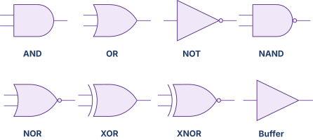
Truth tables of the seven basic gates
The table below lists the truth tables for all seven gates side by side, with the buffer (a non-inverting one-input gate sometimes used as a delay element) included for completeness.
Table 3. Truth tables for the seven basic logic gates plus the non-inverting buffer. The bubble on a NAND, NOR, or XNOR symbol inverts the underlying AND, OR, or XOR output.
| AND | OR | NAND | NOR | XOR | XNOR | NOT | BUF | ||
|---|---|---|---|---|---|---|---|---|---|
| 0 | 0 | 0 | 0 | 1 | 1 | 0 | 1 | 1 | 0 |
| 0 | 1 | 0 | 1 | 1 | 0 | 1 | 0 | 1 | 0 |
| 1 | 0 | 0 | 1 | 1 | 0 | 1 | 0 | 0 | 1 |
| 1 | 1 | 1 | 1 | 0 | 0 | 0 | 1 | 0 | 1 |
XOR is the operation that returns when exactly one of its inputs is . It is also called the exclusive OR. XOR appears throughout digital design as the bit-level adder (producing the sum bit without carry), as the parity check, and as the building block of cryptographic permutations.
Universal gates: NAND and NOR
The set NAND is functionally complete on its own, as is the set NOR. Either gate, replicated, can build AND, OR, and NOT, and from those any function whatsoever. Figure 2 shows the three reductions for NAND.

The proof of universality is direct.
NOT from NAND: tie both NAND inputs together. NAND(, ) = = by the idempotence theorem.
AND from NAND: NAND followed by a NAND-as-NOT. by involution.
OR from NAND: apply De Morgan’s law in reverse. , which is two NAND-as-NOTs feeding a third NAND.
The dual construction with NOR alone is symmetric. NOR is , and the same three reductions work with OR and NOT swapped.
Universality matters in practice because fabricating a single gate type is cheaper than fabricating multiple types. A standard cell library built around a single universal gate cell, plus combinations of that cell, simplifies layout, characterization, and design rule checking. Most modern process node libraries include both NAND and NOR cells, with the choice between them driven by transistor sizing and load characteristics rather than by any logical capability difference.
07.Logic Simplification with Karnaugh Maps
The canonical sum-of-products form from a later section gives one valid expression for a function, but rarely the smallest one. The three-input majority function has a 12-literal canonical SOP and a 6-literal simplified SOP. The difference shows up in silicon as fewer gates, less area, less power, and less delay. Simplification matters.
The 1953 paper by Maurice Karnaugh [3] described a graphical method that handles functions of two through six variables by inspection. The method, the Karnaugh map or K-map, is the workhorse of pencil-and-paper logic simplification and is the standard textbook treatment of the topic. For functions with more variables, the algorithm published by McCluskey three years later [4], together with the modern Espresso heuristic algorithm, takes over.
The K-map idea
A K-map is a two-dimensional table that arranges the input combinations so that cells adjacent in the table differ by exactly one input bit. The arrangement uses Gray code ordering along the axes. The two-bit Gray code is , in which each step flips one bit. The three-bit code extends to . The edges of the map wrap around, so the leftmost column is also adjacent to the rightmost, and the top row is adjacent to the bottom. Adjacency in the K-map corresponds to a single-variable difference between input patterns.
The simplification rule is: any rectangle of adjacent cells, all of which contain a , can be expressed as a single product term with literals. The rectangle’s varying input variables drop out. Only the variables that stay constant across the rectangle appear in the term, complemented or uncomplemented to match the rectangle’s position. Grouping the s into the largest possible such rectangles, and covering every at least once, produces a minimum-cost SOP expression.
2-variable, 3-variable, and 4-variable K-maps
A 2-variable K-map is a grid. The horizontal axis takes the values of and the vertical takes , with the ordering chosen so that adjacent cells differ in one variable.
A 3-variable K-map is a grid. One axis (typically the horizontal) takes and together in Gray-code order . The other axis (vertical) takes .
A 4-variable K-map is a grid with both axes in Gray code: vertically and horizontally. The map wraps around both axes, so the top edge is adjacent to the bottom and the left edge is adjacent to the right.
A 5-variable map is sometimes drawn as two stacked 4-variable maps, but the visual adjacency between the two layers is awkward. A 6-variable map is at the practical limit of what a designer can read at a glance. Beyond that, software is faster and less error-prone than hand-mapping.
Reading groups from a K-map
A valid group on a K-map is a rectangle whose number of cells is a power of two (1, 2, 4, 8, 16, ). Each cell in the rectangle must contain a . The rectangle can wrap around the edges of the map. The goal is to cover every -cell in the map with as few groups as possible, with each group as large as possible.
Each group corresponds to a product term in the simplified SOP. The literals in the term are exactly those input variables that do not change across the group. If is constantly across a group and the other variables vary, the term contains the literal . If is constantly , the term contains . If varies across the group, it does not appear in the term at all.
Don’t-care cells, denoted by an X or d, can be included in a group or excluded from it at the designer’s discretion, whichever produces a smaller expression. Don’t-cares arise when certain input combinations cannot occur (for example, in a BCD-to-decimal decoder the six input combinations through never appear) or when the output value is irrelevant in those cases.
Worked example: simplify the majority function
Figure 3 draws the 3-variable K-map for the majority function, with the four 1-cells marked and three overlapping 2-cell groups identified.
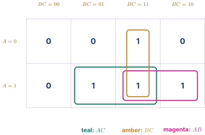
The three two-cell groups together produce the simplified SOP expression
with six literals across three product terms. Comparing the equation above to the canonical form in the equation above, the K-map simplification removes half of the literals and one of the product terms.
Limits of K-maps and a note on Quine-McCluskey
K-maps work well for five or fewer variables. Six variables push the visual format to its limit, and seven or more variables make a hand simplification impractical. For larger functions, the Quine-McCluskey algorithm provides a tabular procedure that handles any number of variables exactly. The procedure generates all prime implicants, then selects a minimum cover using a covering problem. The cost grows exponentially with the number of variables, but the algorithm is deterministic and well-suited to software implementation.
For the very large functions that appear in real circuits (control logic with dozens of inputs, decoders for large instruction sets, PLA programming for finite-state machines), the standard tool is the Espresso heuristic logic minimizer, originally developed at IBM and Berkeley in the 1980s. Espresso does not guarantee a true minimum, but it produces near-optimal results in time that scales gracefully with input size. Modern synthesis tools build on Espresso and on its successors. The Yosys and ABC tools used in the lab chapters include logic minimizers in this family.
08.Multi-Level Logic
A sum-of-products expression maps to a two-level circuit. One level of AND gates feeds one level of OR gates. The depth of the circuit is exactly two. Any function expressible as an SOP can be realized with two gate delays from input to output.
This two-level structure has two costs in practice. First, a function with many wide product terms requires AND gates with many inputs. A typical CMOS standard cell library limits AND fan-in to four or six. Wider ANDs must be broken into a tree of smaller ANDs, which adds depth anyway. Second, the OR gate at the top of the two-level structure may have very many inputs, and a wide OR suffers the same fan-in limit.
Multi-level logic factors a function into a network with more than two levels. The factoring trades depth for gate count. A multi-level realization of a complex function often uses far fewer gates and fewer transistors than the two-level equivalent, at the cost of more gate delays in series along the longest input-to-output path.
Consider the function . The two-level SOP uses four 3-input ANDs and one 4-input OR, with literal inputs. Factoring out of the first three terms gives . The factored form uses one 3-input OR, one 2-input AND, one 2-input OR, and one 2-input AND, plus the outer 2-input AND with . The total is four 2-input gates plus one 3-input OR. That is the same gate count as the two-level version, but only gate inputs against sixteen, and therefore fewer transistors, at the cost of depth four instead of two.
Fan-in and fan-out constraints
The number of inputs a single gate can have is the gate’s fan-in. The number of gate inputs a single output can drive is the fan-out. Both are limited by the physics of the underlying transistor circuit. High fan-in slows the gate because more series transistors increase the path resistance. High fan-out slows the driving gate because more parallel input capacitance increases the load on its output.
Standard cell libraries publish recommended fan-in and fan-out bounds for each cell. Synthesis tools respect these bounds by inserting buffer gates or by restructuring multi-level logic to keep each gate within its recommended range. The fan-in and fan-out discipline is one of the reasons modern synthesized logic ends up with deeper networks than a textbook designer would draw by hand.
Why modern synthesis prefers multi-level
A logic synthesis flow takes a register-transfer-level (RTL) description (Chapter 10) and produces a netlist of standard cells. The synthesis tool’s objective is to meet timing, area, and power constraints simultaneously. Multi-level logic gives the tool more freedom to trade depth against gate count, fan-in against fan-out, and to share intermediate signals across multiple outputs.
Two-level logic is rare in production silicon outside of regular structures such as PLA-based control. Most combinational paths in a modern CPU are several levels deep, with the path depth deliberately tuned to fit inside a single clock cycle at the target frequency. The exact tuning is the subject of Chapter 6 and is one of the central challenges of pipeline design.
09.Standard Combinational Building Blocks
Certain combinational functions show up so often in digital design that they have standardized names, standard symbols, and standard implementations in cell libraries. This section names the most important blocks and gives their truth tables. The structural use of each block appears in later chapters, with multiplexers and decoders driving the datapath of Chapter 25.
Decoders
An -to- decoder takes an -bit input and produces output lines, exactly one of which is at any time. The selected output is the one whose index matches the input value. Decoders are used wherever a numeric input selects a target from among many. Memory address decoders turn an address into a one-hot signal that activates the targeted row of cells (Chapter 43). Instruction decoders turn an opcode into a one-hot signal that activates the targeted functional unit (Chapter 26).
A 2-to-4 decoder has two input bits and four output bits , with when as a binary number and otherwise.
Figure 4 shows the gate-level realization. Each output is the AND of the appropriate combination of or with or , giving four two-input ANDs total.
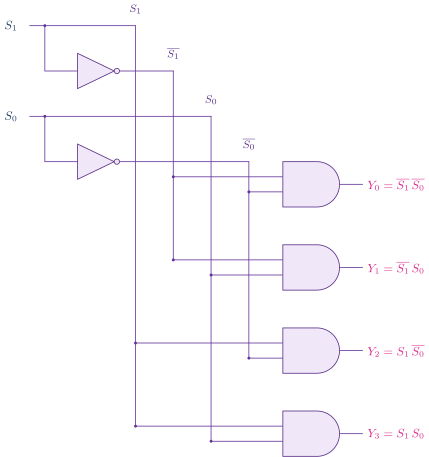
A 3-to-8 decoder follows the same pattern with three input bits and eight 3-input ANDs. An -to- decoder generalizes to -input ANDs and outputs. Most cell libraries provide 2-to-4 and 3-to-8 decoders as single cells, while larger decoders are built from cascades of smaller ones.
Encoders and priority encoders
An encoder is the inverse of a decoder. The -to- encoder takes input lines and produces an -bit output equal to the index of the input that is . The encoder assumes exactly one input is . If more than one input is , the simple encoder produces ambiguous output.
A priority encoder resolves the ambiguity by establishing a fixed priority among the inputs. If multiple inputs are , the output is the index of the highest- priority input that is asserted. Priority encoders are common in interrupt controllers (Chapter 31), where multiple devices may request service simultaneously and the controller must select the highest-priority pending request.
Multiplexers
A multiplexer, abbreviated mux, is the workhorse selector of digital logic. An -to- mux has data inputs, select inputs, and one output. The output equals the data input chosen by the select pattern.
The 2-to-1 mux is the basic case. It has data inputs and , a single select input , and an output given by
The expression itself is a tiny SOP: when the output follows , and when the output follows . A wider mux (4-to-1, 8-to-1, ) generalizes the structure with more data inputs and more select bits. Figure 5 shows a 4-to-1 mux as a tree of three 2-to-1 muxes.
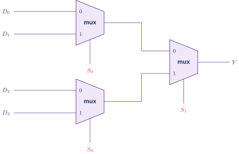
Multiplexers are everywhere inside a CPU. The ALU input mux in Chapter 25 selects between an immediate field and a register file output. The write-back mux selects between the ALU result and a memory-load result. Branch resolution selects between the next sequential PC and a branch target. Modern out-of-order processors layer many additional muxes for operand bypass, register renaming, and tag matching, all built on the same 2-to-1 mux primitive.
Demultiplexers
A demultiplexer, or demux, is the inverse of a multiplexer. The 1-to- demux has one data input, select inputs, and outputs. The selected output equals the data input. The other outputs are . A 1-to- demux is essentially an -output decoder with the single AND of the data input gating each output, and most real designs share the structure between the two functions.
Comparators
A comparator produces a single output bit that is when two multi-bit inputs are equal, or alternatively when one input is less than (or greater than) another. The equality comparator for two -bit values and uses XNOR per bit (XNOR when ) followed by a wide AND of the per-bit results. The magnitude comparator is more involved and is developed in Chapter 5 alongside the simple ALU.
10.Hazards in Combinational Logic
The algebra of the previous sections treats a Boolean expression as an instantaneous function of its inputs. Real circuits do not satisfy that assumption exactly. Each gate has a propagation delay, and the delays along different paths from input to output may differ. As inputs change, the output can transiently take an incorrect value before settling to the correct one. The transient incorrect value is a hazard.
Static-1 and static-0 hazards
A static-1 hazard occurs when the output is supposed to remain at across an input transition, but the actual output dips briefly to during the transition. A static-0 hazard is the dual: the output is supposed to remain at , but it briefly rises to .
The canonical example of a static-1 hazard comes from the expression with the input pattern , , and transitioning from to . Before the transition, and . After the transition, and . The output should stay at throughout.
If the path through is slower than the path through , the second product term drops to before the first product term rises to , and the output briefly drops to before recovering. The brief drop is the static-1 hazard.
Dynamic hazards
A dynamic hazard occurs when the output is supposed to transition once but actually transitions multiple times before settling. Dynamic hazards arise in multi-level circuits with three or more reconvergent paths of different lengths. They are less common than static hazards because most synthesized combinational logic is structured to avoid them, but they can appear in pencil-and-paper designs.
Eliminating hazards: adding consensus terms
The consensus theorem from a later section gives the standard tool for removing static hazards. The expression has the static-1 hazard above. Adding the redundant term produces , which is algebraically the same function but which has a third path from and to the output. The third path covers the brief moment when both of the original product terms are at , holding the output at through the transition. The third term is the consensus term of the original two.
Hazard-free synthesis takes the simplified SOP, identifies input-pair transitions that produce a hazard, and adds back the consensus terms needed to cover those transitions. The cost is extra gates. The benefit is a glitch-free output, which matters for any signal that feeds an edge-triggered storage element. Most modern synthesis tools handle hazard analysis automatically and report which transitions remain unprotected.
For circuits whose outputs feed only edge-triggered flip-flops (Chapter 6), hazards are usually harmless. The flip-flop samples the output once per clock cycle, after the combinational logic has had time to settle. The hazard occurs and resolves within the settling window, and the flip-flop never sees the glitch. For circuits whose outputs feed asynchronous control inputs (a clock enable, a reset, an interrupt input), the hazard discipline is mandatory because the asynchronous logic may sample the glitch and act on it.
11.A Note on Hardware Description
The expressions and gate diagrams in this chapter describe combinational logic at the algebraic and structural levels. Modern design practice describes the same logic in a hardware description language and lets a synthesis tool produce the gate-level netlist. Chapter 10 develops Verilog, SystemVerilog, and Chisel in detail. As a preview, the listing below shows the 3-input majority function in Verilog.
The three-input majority function expressed in Verilog. The continuous-assignment form lets the synthesizer produce gate-level logic that matches the simplified SOP .
| module majority3 ( | |
| input wire A, | |
| input wire B, | |
| input wire C, | |
| output wire M | |
| ); | |
| assign M = (A & B) | (A & C) | (B & C); | |
| endmodule |
A reader curious about how this maps to gates can run it through Yosys with the open-source flow described in Chapter 12. The output netlist is, by default, exactly the three two-input ANDs and one three-input OR of the equation above. The synthesizer can be told to target a specific cell library, in which case the gate-level realization changes to match the available cells, but the function remains the majority of the three inputs in every case.
12.Looking Ahead
The algebra and the gates of this chapter are the substrate on which the rest of the hardware stack is built. The combinational building blocks of Chapter 5 compose into adders, shifters, and multipliers using exactly the gate primitives developed here. The sequential logic of Chapter 6 adds clocked storage on top of combinational networks. The integer ALU sketched in Chapter 5 and built in full in Chapter 11 is a deep multi-level Boolean network. The single-cycle datapath in Chapter 25 stitches together decoders, multiplexers, the ALU, and the register file with the same structural vocabulary introduced in this chapter.
The reader who has worked through the chapter can now read any schematic in the book at the gate level, derive its Boolean function from the gate diagram, simplify the function by K-map for up to four variables, and convert between gate-level and HDL representations of the same logic. These are the durable skills that make every subsequent chapter approachable.
13.Worked Examples
14.Exercises
References
- [1]Boole, George (1854). “An Investigation of the Laws of Thought, on Which Are Founded the Mathematical Theories of Logic and Probabilities.” Walton and Maberly.
- [2]Shannon, Claude E. (1938). “A Symbolic Analysis of Relay and Switching Circuits.” Transactions of the American Institute of Electrical Engineers, 57(12), pp. 713--723. doi:10.1109/T-AIEE.1938.5057767
- [3]Karnaugh, Maurice (1953). “The Map Method for Synthesis of Combinational Logic Circuits.” Transactions of the American Institute of Electrical Engineers, Part I, 72(5), pp. 593--599. doi:10.1109/TCE.1953.6371932
- [4]McCluskey, Edward J. (1956). “Minimization of Boolean.” The Bell System Technical Journal, 35(6), pp. 1417--1444. doi:10.1002/j.1538-7305.1956.tb03835.x