Sequential Logic and Timing
September 13, 202650 min readbeginner
Every circuit in Chapters 4 and 5 is combinational: its output depends only on the current input pattern and changes, after some propagation delay, whenever that pattern changes. There is no yesterday, no…
Every circuit in Chapters 4 and 5 is combinational: its output depends only on the current input pattern and changes, after some propagation delay, whenever that pattern changes. There is no yesterday, no memory, and no concept of “this happened before that.” A real processor cannot work this way. The program counter that steps through instructions must remember which instruction it fetched last. The register file that holds operand values between instructions must preserve those values from one clock cycle to the next. The pipeline registers that separate the five stages of a pipelined CPU (Chapter 29) must latch intermediate results at the end of every clock period and hold them steady while the next stage computes. All of these are sequential circuits, circuits whose output depends on both the current inputs and the stored history of past inputs.
This chapter builds the family of sequential components that every digital system needs: latches, flip-flops, registers, counters, and finite state machines. It then turns to the timing discipline that makes them reliable. A flip-flop that samples data too close to the moment the data changes can produce an output that is neither a clean nor a clean , a phenomenon called metastability. Avoiding metastability requires careful attention to setup and hold times, clock skew, and clock jitter. The chapter closes with the problem of clock domain crossing, the challenge of moving data between parts of a chip that run on independent clocks.
01.From Combinational to Sequential
A combinational circuit implements a Boolean function: for every combination of input values there is exactly one combination of output values, determined entirely by the function and not by anything that happened in the past. The adders, muxes, and decoders of Chapter 5 are all combinational. Their outputs settle to the correct value after the worst-case propagation delay through the gate network and then remain stable as long as the inputs stay fixed.
Consider the stored-program concept introduced in Chapter 1. A program counter (PC) must hold an address, increment it on every clock cycle, and occasionally replace it with a branch target. None of that is possible with combinational logic alone. The PC value at cycle depends on the PC value at cycle , which is a stored quantity, not a direct function of external inputs. The hardware element that stores that value is a register, and the register is built from flip-flops. Before flip-flops, the story begins with latches.
02.Latches
The SR latch
The simplest storage element in digital logic is the SR latch, built from two gates whose outputs feed back into each other’s inputs. Start with two NOR gates arranged so that the output of each gate connects to one input of the other, as shown in Figure 1.
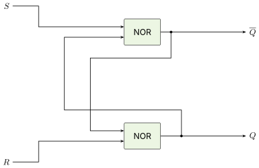
The input drives the upper gate, whose output is , and the input drives the lower gate, whose output is . That pairing is what makes the naming work, because the only way to raise is to force down first, and is the input positioned to do exactly that. A NOR gate outputs only when both of its inputs are . Walk through the input combinations from a concrete starting state. Suppose and (the latch is currently in the reset state).
Set (). Asserting puts a on one input of the upper gate, so that gate’s output falls to and goes from to . The lower gate now sees on one input and on the other. Both of its inputs are , so its output rises to and goes from to . Following that change back around the loop, the upper gate now sees and , so its output remains at and remains at . Nothing further changes, and the latch has settled at , . That is the set state, and it survives returning to , because the upper gate then holds at on the strength of arriving through the feedback path. Applying the same style of reasoning to the other three input combinations gives the complete behavior of the latch:
Table 1. Truth table for the NOR-based SR latch. Q^{+} denotes the next state of Q after the inputs are applied.
| Operation | ||||
|---|---|---|---|---|
| 0 | 0 | Hold (no change) | ||
| 1 | 0 | 1 | 0 | Set |
| 0 | 1 | 0 | 1 | Reset |
| 1 | 1 | 0 | 0 | Forbidden |
When both inputs are , neither gate is forced and the latch retains its previous state. When and , the feedback loop settles with . When and , the loop settles with . The case is forbidden because both NOR outputs go to , violating the invariant that and are complements. Worse, when both inputs return to simultaneously from the forbidden state, the latch enters a race condition whose outcome depends on which gate is fractionally faster. The latch can settle to either state, making the circuit unpredictable.
The D latch
The SR latch stores a bit, but the forbidden input combination is a design hazard. Every circuit that drives an SR latch must guarantee that and are never asserted simultaneously. The D latch eliminates that hazard by deriving both set and reset internally from a single data input and an enable input .
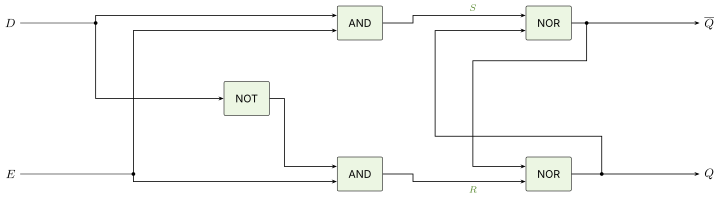
When , both AND gates output regardless of , so the internal SR latch sees and holds its state. When , the upper AND gate passes through as and the lower AND gate passes through as . If then and the latch sets (). If then and the latch resets (). Because and are always complementary when , the forbidden state can never occur.
The key word is transparent. While the enable is high, the D latch behaves like a wire with a small delay. The output follows the input continuously, reflecting every change in until the enable falls.
The transparency problem
Transparency is exactly the property that makes latches unsuitable as the default storage element in a synchronous pipeline. Consider a pipeline with two stages separated by a latch that uses the clock signal as its enable. During the entire high phase of the clock, the latch is transparent. Data from the first stage passes through the latch and enters the second stage. If the second stage computes its result before the clock falls, that result can propagate through the next latch (which is also transparent) and enter the third stage in the same clock cycle. The pipeline discipline is destroyed: data races through multiple stages in a single clock period instead of advancing exactly one stage per cycle.
There is one important exception. A technique called two-phase latch-based clocking uses pairs of latches controlled by non-overlapping clock phases and . The first latch is transparent on and opaque on . The second is the reverse. Because the two phases never overlap, data can advance through exactly one latch per phase, restoring the pipeline discipline. Some high-performance processor designs use this technique because a latch is smaller and faster than a full flip-flop. For the rest of this chapter and for the standard pipeline treatment in Part III, the default storage element is the edge-triggered flip-flop.
03.Flip-Flops
The edge-triggered D flip-flop
The solution to the transparency problem is a storage element that samples its input at a single instant rather than during an entire clock phase. The edge-triggered D flip-flop does exactly that. It captures the value of at the rising (or falling) edge of the clock and ignores all changes in at every other time.
The classic construction is the master-slave arrangement shown in Figure 3. Two D latches are connected in series. The master latch uses the inverted clock as its enable: it is transparent when the clock is low and opaque when the clock is high. The slave latch uses the true clock as its enable: it is transparent when the clock is high and opaque when the clock is low.
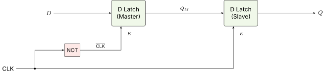
Walk through a rising clock edge with a concrete value. Suppose and the clock is currently low.
-
Clock low. The master latch is transparent (), so the master’s internal storage absorbs . The slave latch is opaque (), so the slave’s output still holds whatever value it stored from the previous cycle.
-
Rising edge. The clock transitions from to . The master’s enable falls to , freezing the master at . Simultaneously the slave’s enable rises to , making the slave transparent. The slave now copies to its output: .
-
Clock high. The master is opaque, so any changes in are blocked at the master’s input. The slave is transparent, but its input () is frozen, so remains stable at .
The net effect is that captures the value of that was present just before the rising edge and holds it for the entire clock period. Changes in after the rising edge do not affect until the next rising edge. That is exactly the one-sample-per-cycle behavior a synchronous pipeline requires.
Other flip-flop types
Textbooks from the 1970s and 1980s devote significant space to the JK flip-flop and the T flip-flop. Both are historically important but have been largely displaced by the D flip-flop in modern design.
The JK flip-flop has two inputs, and . When it sets (). When it resets (). When both are it holds. When both are it toggles (). The JK type eliminates the forbidden state of the SR latch by defining a useful behavior for the case, but the toggle action requires internal feedback that adds delay.
The T (toggle) flip-flop has a single input . When the output toggles on each clock edge. When the output holds. The T flip-flop is simply a JK flip-flop with . It is the natural building block for counters because a free-running T flip-flop with divides the clock frequency by two.
Modern synthesis tools work almost exclusively with D flip-flops. Any JK or T behavior is expressed by placing combinational logic in front of a D flip-flop: for JK semantics, or for T semantics. This approach gives the synthesizer maximum flexibility to optimize the surrounding logic, which is why design libraries and FPGA primitives overwhelmingly offer D flip-flops with optional clock enable, set, and reset inputs.
Flip-flop with enable, preset, and clear
A bare D flip-flop samples on every clock edge. Practical designs often need three additional controls:
-
Clock enable (CE). When the flip-flop ignores the clock edge and holds its current value. When the flip-flop operates normally. A flip-flop with clock enable is equivalent to a mux in front of the input: .
-
Asynchronous clear (CLR). Forces immediately, regardless of the clock. Used to put the circuit into a known state at power-on or after a system reset.
-
Asynchronous preset (PRE). Forces immediately, regardless of the clock. Less common than clear but occasionally needed.
The question of whether to use synchronous reset (reset is sampled at the clock edge, like ordinary data) or asynchronous reset (reset overrides the clock and takes effect immediately) is one of the enduring debates in digital design. Asynchronous reset is simpler to reason about during power-on because it does not need a running clock. On the other hand, deasserting an asynchronous reset too close to a clock edge can itself cause metastability. Many design teams compromise: assert reset asynchronously (so the circuit enters a known state even before the clock stabilizes) and deassert it synchronously (synchronized to the clock to avoid the metastability hazard on the release edge). The flip-flop primitive then carries an asynchronous reset input whose deassertion is managed externally by a reset synchronizer circuit, a concept revisited in a later section.
04.Registers and Register Files
Parallel-load registers
A register is a group of flip-flops that share a common clock and store a single multi-bit value. An -bit register holds one -bit word. Each flip-flop in the register stores one bit of the word. On every active clock edge, all flip-flops sample their respective data inputs simultaneously, and the entire word updates in one cycle.
A register with a load enable signal adds a mux in front of each flip-flop’s input. When , the mux routes the external data to . When , the mux feeds the flip-flop’s own output back to its input, so the stored value is retained. This is exactly the clock-enable technique from the previous section applied to the entire register.
Shift registers
A shift register is a chain of flip-flops in which the output of each flip-flop connects to the data input of the next. On each clock edge the stored pattern shifts one position down the chain, and a new bit enters from one end.

Four configurations are common:
-
Serial-in, serial-out (SISO). Data enters one bit per clock cycle at one end and exits one bit per cycle at the other. The register acts as a delay line that holds bits in flight.
-
Serial-in, parallel-out (SIPO). Data enters serially but all bits are available simultaneously at the parallel outputs. Used to convert a serial data stream (from a UART, SPI bus, or IC bus) into a parallel word.
-
Parallel-in, serial-out (PISO). An entire -bit word is loaded in parallel on one clock edge and then shifted out one bit at a time on subsequent edges. Used for the transmit side of a serial interface.
-
Bidirectional. A control signal selects whether the pattern shifts left or right on each clock edge.
Linear feedback shift registers
A linear feedback shift register (LFSR) is a shift register whose serial input is an XOR (or XNOR) of selected output bits called taps. With the right choice of taps, an -bit LFSR cycles through all nonzero states before repeating (the all-zeros state is a fixed point of the XOR feedback and is excluded). The maximal-length tap polynomials are well tabulated.
LFSRs are used for cyclic redundancy checks (CRC) in networking hardware, for pseudo-random pattern generation in built-in self-test (BIST) circuits that exercise a chip after fabrication, and for scrambling bits on high-speed serial links to maintain DC balance.
A glimpse of the register file
The register file inside a CPU is a small, fast memory that holds the architectural registers named by the instruction set. A simple register file with registers, each bits wide, two read ports, and one write port is built from three components:
-
A bank of parallel-load registers (the storage).
-
A -to- decoder that selects which register receives the write data on a write enable.
-
Two -to- multiplexer arrays (each bits wide) that select the read data for the two read addresses.
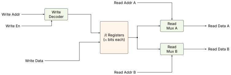
The register file is the most heavily accessed structure in a processor’s datapath. In a single-cycle CPU (Chapter 25) it is read twice and written once every cycle. In an out-of-order superscalar core (Chapter 51) the physical register file may have six or more read ports and three or more write ports. Each read port adds one more mux array and each write port one more decoder, so those structures grow linearly with the port count, while the storage array itself grows faster, because every additional port adds a word line and a bit line to every cell and the cell area rises roughly with the square of the total number of ports. The basic principle, however, is the same register-plus-mux structure of Figure 5 scaled up.
05.Counters
A counter is a sequential circuit that steps through a defined sequence of states. The most common form is the binary counter, which counts and then wraps back to . Counters appear in program counters, memory address generators, timer peripherals, and performance monitoring hardware.
Ripple (asynchronous) counters
The simplest binary counter chains T flip-flops in series. The first flip-flop toggles on every external clock edge, dividing the frequency by two. The second flip-flop is clocked by the first’s output and divides by two again, producing a frequency of . The pattern continues: the -th flip-flop produces .
The output bits of the chain form a binary count, but with an important caveat. Each flip-flop triggers on the output transition of the preceding flip-flop, so the toggle propagates through the chain like a ripple through water. After the external clock edge there is a brief interval during which the counter’s output bits are changing one at a time from LSB to MSB. The total settling time is , where is the clock-to-Q delay of one flip-flop. During that interval the output can momentarily show a value that is not the old count and not the new count, a transient glitch that can cause downstream logic to malfunction if sampled at the wrong instant.
Synchronous counters
A synchronous counter clocks every flip-flop from the same external clock signal. The next count value is computed by combinational logic that reads the current count and produces the next count. All flip-flops update simultaneously on the clock edge, so the output transitions from the old count to the new count in a single delay with no intermediate glitches.
For a binary up-counter, the next-state logic for bit is:
Bit toggles every cycle. Bit toggles when bit is . Bit toggles when bits and are both . The product term grows with , so the combinational depth is for an -bit counter. For wide counters at high clock frequencies, the carry chain through the AND product can become the critical path. The same carry-lookahead techniques used in adders (a later section in Chapter 5) can be applied to the counter’s enable chain, trading area for speed.
An up/down counter adds a direction control bit . When the counter increments. When it decrements. The next-state logic uses the generate signal from an adder/subtractor to compute the correct toggle conditions in both directions.
A modulo- counter counts from to and then resets to on the next clock edge. When is a power of two, the counter wraps naturally. When is not a power of two, a comparator detects the terminal count and forces the next state to zero.
Ring and Johnson counters
A ring counter is a shift register with its serial output connected back to its serial input. If the register is loaded with a single bit and the remaining bits are , the lone circulates around the loop, visiting each flip-flop in turn. An -bit ring counter has states, one per flip-flop, producing a one-hot output that is useful for sequencing control signals.
A Johnson counter (also called a twisted ring counter) connects the complement of the last flip-flop’s output back to the first flip-flop’s input. An -bit Johnson counter cycles through distinct states. For example, a 4-bit Johnson counter visits the sequence . Adjacent states differ in exactly one bit (a Gray-like property), which makes Johnson counters attractive for generating timing phases and for clock-domain crossing pointer encoding, a topic revisited in a later section.
06.Finite State Machines
The state machine abstraction
Every sequential circuit described so far, latches, flip-flops, counters, shift registers, can be viewed as a special case of a more general abstraction: the finite state machine (FSM). An FSM is defined by five quantities:
-
: a finite set of states.
-
: a finite set of inputs.
-
: a finite set of outputs.
-
: the next-state function, .
-
: the output function, whose form distinguishes the two major FSM types.
A state diagram represents the FSM as a directed graph. Each node is a state. Each directed edge is a transition labeled with the input (and possibly the output) that triggers it. The FSM starts in a designated initial state and transitions to a new state on each clock edge according to the current state and the current input.
Moore machines
In a Moore machine the output depends only on the current state: . The output is written inside or next to the state node in the state diagram, not on the transition edges. Because the output changes only when the state changes, and the state changes only on a clock edge, Moore outputs are inherently synchronous and glitch-free.
Worked example: 1011 sequence detector (Moore). Design an FSM that asserts its output for one clock cycle whenever it detects the input sequence on a serial input line . The detector allows overlapping sequences: if the input stream is , the output asserts twice.
Build the state diagram step by step. The machine needs to remember how much of the target pattern it has seen so far.
-
: no part of the pattern has been matched. Output .
-
: the most recent input was (first bit of ). Output .
-
: the two most recent inputs were . Output .
-
: the three most recent inputs were . Output .
-
: the four most recent inputs were . Output (pattern detected).
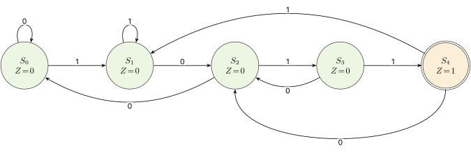
The backward transitions require careful thought. When the machine is in (having seen ) and the input is , the last two inputs form the subsequence , which matches the first two bits of the target pattern. The machine therefore transitions to , not all the way back to . When the machine reaches and the next input is , that single could be the start of a new match, so the machine goes to . This overlap handling is essential for detecting patterns like where the trailing shares the leading with the previous match.
Mealy machines
In a Mealy machine the output depends on both the current state and the current input: . The output is written on the transition edges of the state diagram, not inside the state nodes.
The same 1011 detector as a Mealy machine. Because the output can react to the current input within the current state, the Mealy machine often needs one fewer state to express the same behavior.
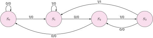
The Mealy machine uses four states instead of five. State encodes “I have seen so far.” When the next input is , the Mealy machine emits on the transition itself and moves to (the trailing could begin a new match). The Moore machine needed a separate state whose sole purpose was to hold for one cycle.
Table 2. Comparison of Moore and Mealy machines for the 1011 sequence detector.
| Property | Moore | Mealy |
|---|---|---|
| States needed | 5 | 4 |
| Output changes | On clock edge only | Between clock edges |
| Output glitches | None (synchronous) | Possible (combinational) |
| Output timing | One cycle delayed | Same cycle |
The Mealy machine’s output can react faster because it does not need to wait for the state register to update. However, the output is a combinational function of the current input, which means it can glitch if the input changes at an unexpected time. In practice, many designers register the Mealy output (pass it through a flip-flop) before sending it to the rest of the circuit, which eliminates the glitch risk at the cost of one cycle of latency. A registered Mealy machine behaves identically to the corresponding Moore machine from the perspective of downstream logic.
State encoding
An FSM with states needs a state register wide enough to represent all states. The encoding of states into binary patterns affects the cost and speed of the next-state and output logic.
Binary encoding. Use flip-flops and assign states as consecutive binary numbers: , , , for a 4-state machine. This minimizes the number of flip-flops but produces next-state logic with more terms because each bit participates in multiple state transitions.
One-hot encoding. Use flip-flops, one per state. In any given cycle exactly one flip-flop holds a and the others hold . The next-state logic for each flip-flop depends only on the subset of transitions that enter its state, which is often just one or two product terms. One-hot encoding wastes flip-flops (an FPGA has them in abundance) but produces very fast, shallow combinational logic.
Gray encoding. Adjacent states in the sequence differ in exactly one bit. Useful when the output is decoded directly from the state register and the designer wants to minimize the number of output bits that change on any single transition, reducing glitch risk on the output lines.
Table 3. State encoding tradeoffs for an FSM with k states.
| Encoding | Flip-flops | Next-state logic | Best for |
|---|---|---|---|
| Binary | Deeper | ASICs (area) | |
| One-hot | Shallower | FPGAs (speed) | |
| Gray | Moderate | Glitch-free outputs |
FPGA synthesis tools typically default to one-hot encoding because the flip-flops come “for free” in the FPGA fabric and the shallow next-state logic runs faster. ASIC synthesis tools lean toward binary or Gray encoding to minimize silicon area. Most modern tools let the designer choose or allow the tool to select the encoding that meets timing with the smallest area.
FSMs in hardware description languages
A hardware description language expresses a Moore or Mealy FSM as two blocks of logic: one for the next-state function and one for the output function. In SystemVerilog the state register is an always_ff block that updates on the clock edge, while the next-state and output functions are always_comb blocks. In Chisel the state register is a RegInit value and the combinational logic is a switch on the state.
Moore 1011 detector in SystemVerilog (abbreviated)
typedef enum logic [2:0] {
  S0, S1, S2, S3, S4
} state_t;

state_t state, next_state;

always_ff @(posedge clk or posedge rst)
  if (rst) state <= S0;
  else     state <= next_state;

always_comb begin
  next_state = state;
  case (state)
    S0: next_state = x ? S1 : S0;
    S1: next_state = x ? S1 : S2;
    S2: next_state = x ? S3 : S0;
    S3: next_state = x ? S4 : S2;
    S4: next_state = x ? S1 : S2;
  endcase
end

assign z = (state == S4);
The assign z line implements the Moore output: depends only on the state, not on the input . Chapter 10 develops hardware description languages in full. The snippet here is a preview meant to connect the abstract state-diagram notation to concrete RTL code.
07.Timing Constraints
The flip-flops and registers of the previous sections work correctly only if the data arriving at each flip-flop’s input is stable for long enough around the clock edge. This section makes that requirement precise.
Setup time, hold time, and clock-to-Q
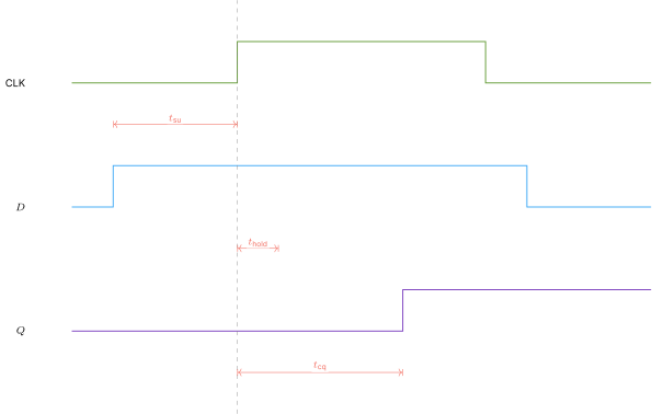
Every edge-triggered flip-flop has three fundamental timing parameters.
Use a concrete example. A flip-flop in a modern 7 nm process might have ps, ps, and ps. The data must be settled at least 30 ps before the clock edge and must not change until at least 10 ps after the clock edge. The new output appears 40 ps after the edge.
The critical path and maximum clock frequency
A synchronous circuit is a chain of flip-flops separated by combinational logic. On each clock edge, every flip-flop captures its new input. The combinational logic between two adjacent flip-flops must settle before the next clock edge so that the receiving flip-flop’s setup time is satisfied.
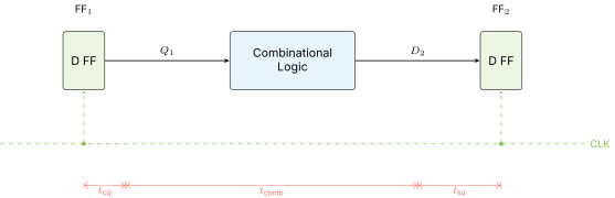
The clock period must satisfy the setup constraint:
The critical path is the longest combinational delay between any pair of flip-flops in the entire design. It determines the maximum clock frequency:
Hold-time violations and short paths
The setup constraint limits the maximum clock frequency. A second constraint, the hold constraint, is independent of the clock period and therefore cannot be fixed by slowing the clock.
The hold constraint requires that the data at the capturing flip-flop’s input must not change too soon after the clock edge. If the combinational path from the launching flip-flop to the capturing flip-flop is very short, the new data from the launching flip-flop’s can arrive at the capturing flip-flop’s before the hold window has closed. The constraint is:
Here is the shortest combinational delay between the two flip-flops. If this inequality is violated, the new data corrupts the capture of the old data. The result is a hold-time violation, which produces unpredictable behavior and is not recoverable by changing the clock frequency.
In modern processes the flip-flop’s own is usually large enough relative to that hold violations are rare on paths with any combinational logic at all. The dangerous case is a direct flip-flop-to-flip-flop connection with no intervening logic, where and the hold check reduces to . If the process library guarantees this inequality (most do for same-clock flip-flops on the same voltage rail), direct connections are safe.
Clock skew and clock jitter
The analysis above assumes the clock arrives at both flip-flops at exactly the same instant. In a real chip the clock signal travels through a distribution tree (buffers, wires, sometimes a clock mesh), and the arrival time varies from flip-flop to flip-flop.
Clock skew () is the difference in clock arrival time between the launching and capturing flip-flops. If the capturing flip-flop’s clock arrives earlier than the launching flip-flop’s clock by an amount , the effective time available for the combinational logic is reduced by .
The setup constraint with skew becomes:
The hold constraint also changes. If the capturing flip-flop’s clock arrives later than the launching flip-flop’s clock, the hold window shifts later, tightening the hold budget. The hold constraint with skew becomes:
Clock jitter () is the cycle-to-cycle variation in the clock period caused by noise in the clock source (PLL, oscillator) or in the distribution network. Jitter adds to the uncertainty in both the setup and hold margins. In a first-order analysis, the setup constraint incorporates jitter as an additional penalty:
Clock distribution design, including clock trees, clock meshes, and useful skew scheduling, is a major topic in physical design and timing closure. The key takeaway for this chapter is that every picosecond of skew and jitter subtracts directly from the time budget available to the combinational logic, reducing the maximum clock frequency.
08.Metastability
The metastable state
Every flip-flop has three possible output states: a valid , a valid , and a third possibility that the datasheet does not advertise. When the data input changes during the setup/hold window, the flip-flop’s internal feedback loop can settle at a voltage between the valid logic levels. This intermediate voltage is the metastable state.
Think of a ball balanced on top of a hill. The two valleys on either side of the hill represent the valid and valid states. Any small perturbation pushes the ball into one valley or the other, but if the ball is placed precisely on the hilltop, it can linger there for an unpredictable amount of time before eventually falling to one side. The flip-flop’s internal cross-coupled inverter pair behaves the same way. When the data transition falls within the setup/hold window, the inverter pair is driven toward the unstable midpoint between its two stable operating points.
The resolution time is governed by an exponential decay. Let be the time constant of the flip-flop’s regenerative feedback loop (a property of the transistor technology and the flip-flop design). The rate at which the flip-flop enters the metastable state and is still unresolved after a resolution time is:
where is a technology-dependent constant with units of seconds (related to the size of the setup/hold window), is the clock frequency, and is the rate at which the asynchronous input changes. Note the units. The product is seconds times hertz times hertz, which is one over seconds, so the left side of the equation counts failures per second rather than giving a dimensionless probability. The mean time between failures (MTBF) is the reciprocal of that failure rate:
The exponential in the numerator is the key. Increasing the resolution time by a few multiples of raises the MTBF by orders of magnitude. If ps and (a 1 GHz clock sampling a 100 MHz asynchronous signal with ns), then a resolution window of ps () yields:
That is far too low. Increasing to 800 ps ():
Doubling the resolution window from 400 ps to 800 ps transformed the MTBF from seconds to decades. This dramatic improvement is why the standard mitigation is simply to allow the flip-flop more time to resolve, which is exactly what a synchronizer does.
Synchronizers
A synchronizer is a chain of two or more flip-flops with no combinational logic between them. The first flip-flop in the chain samples the asynchronous input and may go metastable. The second flip-flop does not sample the asynchronous input directly. It samples the first flip-flop’s output, which has had an entire clock period (minus the second flip-flop’s own setup time) to resolve from any metastable state.
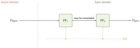
The resolution time available to FF is one full clock period minus FF’s setup time:
Substituting into the MTBF formula:
For safety-critical applications (automotive, aerospace, medical devices) the two-stage synchronizer may not provide a high enough MTBF. Adding a third flip-flop in the chain gives the metastable signal two full clock periods to resolve (minus two setup times), increasing the MTBF by another exponential factor. Each additional stage adds one cycle of latency.
The synchronizer’s effectiveness depends on having no combinational logic between the two flip-flops. Any logic between them eats into the resolution time , degrading the MTBF. This is why synthesis tools and design-rule checks flag logic inserted between synchronizer stages as a critical violation.
09.Clock Domain Crossing
Why multiple clock domains exist
A modern SoC rarely runs on a single clock. The CPU core might run at 3 GHz. The memory controller at 1.5 GHz. The USB controller at 480 MHz. The IC peripheral at 400 kHz. Each of these subsystems is a separate clock domain: a group of flip-flops driven by the same clock signal, with guaranteed timing relationships among them. Within a clock domain, setup and hold analysis is straightforward because every flip-flop sees the same clock (modulo skew). Between clock domains, there is no guaranteed phase or frequency relationship, so every signal crossing from one domain to another must be synchronized.
The reasons for multiple domains include:
-
Power. Running a subsystem at the lowest clock frequency that meets its throughput requirement saves dynamic power, which is proportional to frequency.
-
IP reuse. Pre-designed intellectual property blocks (USB PHY, PCIe endpoint, DDR controller) ship with their own clock requirements. Forcing them onto the SoC’s core clock would break their internal timing.
-
Interface standards. External interfaces (Ethernet at 125 MHz, HDMI at pixel clock, PCIe at 250 MHz per lane) define their own clocks that the SoC must receive.
Single-bit crossing with synchronizers
For a single-bit control signal crossing from one domain to another, the two-flip-flop synchronizer of a later section is the standard solution. The signal enters the first flip-flop clocked by the destination domain’s clock, passes through the second flip-flop one cycle later, and emerges as a safely synchronized signal in the destination domain.
One subtlety arises when a fast-domain signal must be seen by a slow-domain clock. If the fast-domain signal is asserted for only one fast-domain cycle, it may be too short for the slow-domain synchronizer to sample. The standard fix is pulse stretching: the fast domain holds the signal asserted until the slow domain acknowledges receipt, or stretches it to at least 1.5 slow-domain clock periods, guaranteeing that the slow-domain synchronizer sees at least one full asserted sample.
Multi-bit crossing with handshake and FIFO
Synchronizing a multi-bit bus one bit at a time does not work. Each bit passes through its own synchronizer and may resolve on different clock edges, producing a momentary corrupted value at the output. If the bus transitions from to , and the MSB synchronizes one cycle before the lower three bits, the destination domain briefly sees , a value that was never sent.
Two standard solutions exist:
Handshake protocol. The source domain places the multi-bit data on a bus and asserts a single-bit req signal. The destination domain synchronizes req, captures the bus (which is stable because the source is waiting), and asserts a single-bit ack back to the source domain. The source domain synchronizes ack and knows it is safe to change the bus. The protocol ensures that the multi-bit bus is stable whenever it is sampled, at the cost of several round-trip synchronization latencies.
Asynchronous FIFO. An asynchronous FIFO decouples the two clock domains with a shared memory buffer. The source domain writes data into the FIFO at its own clock rate. The destination domain reads data out at its own clock rate. The FIFO’s write pointer and read pointer each live in their respective clock domains. To compare the pointers (for full and empty detection), each pointer is encoded in Gray code before crossing to the other domain. Gray code guarantees that only one bit changes per increment, so the synchronized pointer in the other domain is either the current value or the previous value, never a corrupted intermediate. The worst case is a one-cycle-old pointer, which means the FIFO may report “full” one cycle late or “empty” one cycle late, a conservative error that never loses data.
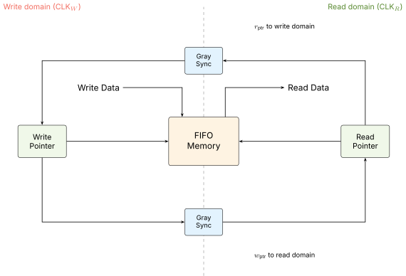
The Gray code encoding for the pointers uses bits for a FIFO of depth (the extra bit distinguishes “full” from “empty” when the read and write pointers are equal). Gray-code ordering was introduced in Chapter 4 as the axis ordering that makes adjacent K-map cells differ in one bit. Converting an -bit binary value to Gray code uses the same one-bit-change property and is a single row of XOR gates, and for . The Johnson counter of a later section also has the single-bit-change property and serves a similar role in some FIFO designs.
Clock domain crossing is one of the most error-prone areas of digital design. Verification tools such as CDC checkers (Synopsys SpyGlass CDC, Cadence Conformal CDC) exist specifically to flag signals that cross between clock domains without proper synchronization. Clock domain crossing at the system level, between memory controllers, I/O links, and multicore interconnects, lies beyond this book.
10.Looking Ahead
This chapter has moved from combinational logic to sequential logic, introducing the storage elements (latches and flip-flops), the standard sequential building blocks (registers, shift registers, counters, finite state machines), and the timing discipline (setup/hold, metastability, synchronizers, clock domain crossing) that makes them reliable. Every clocked element in the rest of the book, from the pipeline registers of Chapter 29 to the reorder buffer entries of Chapter 52, rests on the D flip-flop and the timing analysis developed here.
Chapter 7 turns to the arithmetic circuits that sit between the flip-flops: multipliers, dividers, and modular-arithmetic units. Where Chapter 5 built adders, subtractors, and shifters as combinational blocks, the next chapter shows how multiplication and division decompose into multi-cycle sequences of additions and shifts controlled by a small FSM. The sequential logic of this chapter and the combinational arithmetic of the previous two chapters combine to form the integer execution unit at the heart of every CPU.