Trends, Constraints, and Quantitative Principles
September 13, 202649 min readbeginner
Computer architecture is a quantitative discipline. Every design choice in the field, from the depth of a pipeline to the width of a memory bus, is justified by a number. The number measures performance…
Computer architecture is a quantitative discipline. Every design choice in the field, from the depth of a pipeline to the width of a memory bus, is justified by a number. The number measures performance, power, area, cost, reliability, or some combination of these against a baseline. This chapter establishes the quantitative vocabulary and the analytical tools the rest of the book uses to make and evaluate those measurements. The first half surveys the technological trends and design constraints under which modern architects work. The second half develops the methodology of performance measurement and the five quantitative principles that have proven most useful in design. The chapter is denser with formulas and derivations than any other in Part I, in keeping with its companion role to the qualitative introduction in Chapter 1.
01.Why Architecture Is a Quantitative Discipline
A designer who has just finished building a new processor needs to answer a single question for every potential customer. Is this machine better than the alternative? The word better hides almost the entire field of computer architecture. Better at what? Better by how much? Better at what cost? The honest answer is always a number with units, measured against a competitor or against the same architect’s previous design.
The reason this matters is that nearly every architectural idea has a cost. A wider issue width lets a processor execute more instructions per cycle, but the additional execution units take silicon area, raise the clock-load on each register, and burn power even when idle. A larger cache reduces the rate of misses that go to main memory, but the cache itself takes area, takes power, and increases the latency of every access. A more aggressive branch predictor recovers from fewer mispredictions but costs storage. Nothing is free. The discipline is the habit of insisting on a quantitative justification for each addition and the habit of measuring, after the design is built, whether the justification held up.
Quantitative reasoning also serves a second purpose. It makes architectural claims comparable across machines and across time. A statement like “the Apple M3 has a six-wide decoder” is a fact about microarchitecture. A statement like “the Apple M3 runs SPECint at 9.8 score units per watt, compared with 7.1 for the Intel Raptor Lake i9” is a quantitative claim that can be verified and that has consequences for system design. The book’s exercises and case studies favor the second kind of statement. Numbers settle arguments that adjectives cannot.
The rest of this chapter develops the tools needed to make quantitative claims that survive scrutiny. A later section sets out the constraints architects work within. A later section survey the trends in technology, power, cost, and dependability that drive design choices over time. A later section build the methodology of performance measurement, benchmarking, and result summarization. A later section collects the five principles of design that have proven most useful, with full derivations of Amdahl’s law and the processor performance equation.
02.Design Constraints and Tradeoffs
A computer architect designs against four primary constraints. They are performance, power, area, and cost. Reliability, security, and time to market are secondary constraints that exert pressure on the first four. This section enumerates the four primary constraints, the units in which each is measured, and the way design choices trade them against one another.
Performance, power, area, and cost
Performance is what the customer cares about most directly. The customer wants the program to finish in less wall-clock time, or to handle more requests per second, or to feel responsive under interactive load. Performance is measured in time per operation (latency) or in operations per unit time (throughput). The two are not interchangeable. A system that processes one request in 100 ms has the same throughput as one that serves ten requests together over one second, but the first feels ten times as responsive to a user typing, because each of its requests finishes in 100 ms rather than at the end of a full second.
Power is what the customer cares about second. Battery-powered devices live and die by power. Datacenter operators pay an electricity bill that often exceeds the capital cost of the hardware over a server’s lifetime. Power is measured in watts (W) of instantaneous dissipation or in joules per operation. The two are related through frequency. A 100 W processor running for 10 seconds dissipates 1000 joules of energy regardless of how that work is divided across cycles.
Area is what the manufacturer cares about. Silicon costs money per square millimeter, and each chip must fit on a wafer. Area is measured in square millimeters of die, sometimes converted to transistor count via a process-dependent density. A 2026-era die typically holds 30 to 100 billion transistors on 300 to 800 square millimeters.
Cost is what everyone cares about in the end. Cost is measured in dollars per unit, with the convention that bulk pricing applies above some volume threshold. A high-end smartphone SoC costs the device maker roughly $50 to $200 per unit in 2026. A datacenter server CPU costs $3000 to $15,000.
The architecture-circuit-software co-design surface
The four constraints interact through three layers. They are the architecture, the circuit implementation, and the software workload. A decision at any one of the three can be undone at another. A microarchitectural decision to double the cache size raises power and area but reduces miss-rate-driven performance loss. A circuit decision to lower the supply voltage saves power but slows the gates and may force a frequency reduction. A software decision to vectorize a loop exploits hardware features the architect already paid for in area and power.
This three-layer optimization is called architecture-circuit-software co-design. The architect’s job is rarely to optimize a single layer in isolation. It is to find combinations of choices across the three layers that meet the customer’s actual constraint, which is usually performance per watt per dollar on a workload the customer actually runs.
03.Trends in Technology
The constraints in the previous section do not stay fixed across years. They move as semiconductor technology evolves. This section covers the two trend curves that shaped computer architecture from 1970 to about 2005, and the breakdown of one of them around 2005 that defined the field’s last twenty years.
Moore’s Law
In a four-page article in Electronics magazine in April 1965, Gordon Moore observed that the number of transistors economically integrated on a single die had been doubling roughly every year since the integrated circuit was invented in 1958 [1]. Moore predicted that the doubling would continue for at least another decade. In 1975 he revised the estimate to doubling every two years. Moore’s law is the name the industry has used ever since for the trend.
The empirical history bears out the prediction with remarkable fidelity. The Intel 4004 of 1971 had 2300 transistors. The Intel 8086 of 1978 had about 29 000. The 80386 of 1985 had 275 000. The Pentium of 1993 had 3.1 million. The Pentium 4 of 2000 had 42 million. The NVIDIA H100 of 2022 had about 80 billion. The AMD MI300X of 2023 had about 153 billion. The total span is over seven orders of magnitude across roughly fifty years. Figure 1 plots these data points alongside a reference line for the “doubling every two years” prediction.
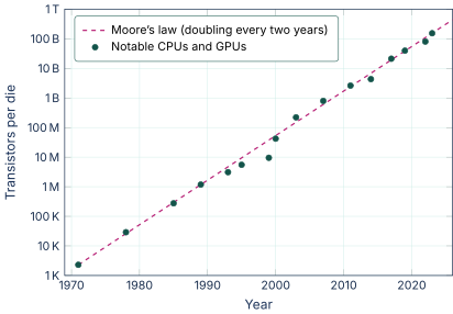
Moore’s law is an economic observation, not a physical law. The doubling continues only as long as it remains economically profitable to invest in the next process node. The doubling interval has stretched in recent years from twenty-four to about thirty-six months, partly because each new node costs vastly more to develop than the previous one (a 2 nm fabrication facility in 2026 costs roughly $20 billion to build), and partly because the physical headroom for further shrinks is running out. The trend continues as of 2026 but is widely expected to slow further toward the end of the decade.
Dennard scaling and its end
Moore’s law tells the architect how many transistors are available. Dennard scaling, after Robert Dennard’s 1974 paper at IBM [2], tells the architect what each of those transistors costs in power. The paper laid out the rules for shrinking an MOS transistor while keeping the surrounding design unchanged. If the linear dimensions of the transistor (gate length, gate width, oxide thickness) shrink by a factor , and the supply voltage shrinks by the same factor , then several quantities follow.
Begin with the per-transistor gate capacitance. The gate capacitance of an MOS transistor is proportional to the gate area divided by the oxide thickness. Gate area scales as and oxide thickness scales as , so
The transit time across the channel shrinks as in Dennard’s scaling regime, so the maximum switching frequency scales as
The dynamic switching power of a transistor toggling at frequency is . Substituting the scaled quantities,
Each transistor dissipates times less power than before the shrink. Now consider the chip as a whole. The number of transistors per unit area scales as since each transistor is times smaller in each linear dimension. Power per unit area is the product,
The equation above is the central Dennard result. As long as voltage shrinks proportionally with linear dimensions, power density stays constant from one process generation to the next. A chip with twice the transistor count, running at twice the frequency, dissipates the same power per square millimeter. The total power of a fixed-area die remains unchanged.
Dennard scaling held remarkably well for thirty years. From the early 1970s through the mid-2000s, each process generation roughly halved feature sizes, doubled transistor count per unit area, increased frequency, and kept chip-wide power within a steady budget. The combined effect, multiplied across thirty years, produced more than a million-fold improvement in performance per watt.
The break came around 2005. The supply voltage stopped shrinking. The reason is leakage current. Modern MOS transistors have a sub-threshold leakage that grows exponentially as the threshold voltage approaches zero. Maintaining an acceptable on-off ratio requires to stay above roughly 200 to 300 mV. Since cannot reasonably operate at less than about , the supply voltage hit a floor near 0.7 to 1.0 V. Further dimensional shrinking continued, but voltage stopped following.
With no longer scaling, repeat the derivation. Per- transistor power becomes
Each transistor now dissipates the same power as before the shrink, not less. Power per unit area becomes
Each process generation now doubles the power per unit area. A chip designed at twice the transistor density of its predecessor, at the same frequency, dissipates twice the power per square millimeter. The chip-wide power budget cannot follow that curve. The thermal envelope of a personal computer is roughly 150 W and that of a server CPU is roughly 350 W. These limits are set by what air or liquid cooling can extract from a few hundred square millimeters of die. The end of Dennard scaling was therefore the end of unconstrained frequency growth. Architects responded by capping frequency, leaving large portions of the die dark on any given cycle (the dark silicon problem), and shifting work onto parallel cores and accelerators where energy per operation is lower. The rest of this book is, in large part, a story about that shift.
Scaling of transistor performance and wires
Inside the transistor, switching speed has continued to improve with each shrink, though more slowly than Dennard’s pure scaling predicted. Outside the transistor, the wires that connect transistors have scaled less favorably. A wire’s resistance per unit length grows as cross-section shrinks (resistance ), while its capacitance per unit length to nearby wires stays roughly constant. The RC product per unit length therefore grows with each shrink, and the delay of a long wire grows quadratically with its length. By 2010, signal propagation across a large die was already comparable in cost to several gate delays. Modern architects route critical signals through repeaters, shorten paths by partitioning logic into adjacent regions, and pipeline long wires. The deeper treatment is in Chapter 9 (Part I’s chapter on From Logic to Silicon). The takeaway for this chapter is that transistor and wire scaling do not move together, so the architect cannot assume that everything inside a chip gets faster at the same rate.
Memory and storage technology trends
DRAM density has historically tracked Moore’s law, doubling every two to three years. DRAM access latency has improved much more slowly, roughly 10 to 20 percent per decade. The growing latency gap between processor and memory is the memory wall, a topic to which Part IV returns in depth. SRAM, the technology used for on-chip caches, scales similarly to logic transistors and so tracks density improvements but not latency improvements.
Storage technology has been less predictable. Hard disks doubled density roughly every two years from 1990 through 2010 but have plateaued since, with shingled-magnetic-recording and helium- filled drives delivering incremental gains. Flash memory replaced hard disks in personal computing during the 2010s. NAND flash density has continued to scale by stacking layers vertically (3D NAND now exceeds 200 layers in 2026). Storage-class memory technologies such as Intel’s now-retired 3D XPoint, Samsung’s HBM-PIM, and various phase-change candidates have tried to fill the gap between DRAM and flash. None has yet achieved both the price and the longevity needed to fully replace either neighbor.
Performance trends: bandwidth over latency
A consistent pattern across half a century of computing, made explicit by David Patterson’s 2004 article Latency Lags Bandwidth [3], is that bandwidth has grown roughly an order of magnitude faster than latency for almost every component of the system. Disk bandwidth grew 100 times faster than disk seek latency from 1980 to 2020. Network bandwidth (per dollar) grew 1000 times faster than network round-trip latency over the same period. DRAM bandwidth, through wider buses and channels, has grown roughly 30 times more than DRAM access latency.
The architectural consequence is that modern systems are overwhelmingly bandwidth-limited rather than latency-limited. Throughput-oriented workloads (GPUs running matmul, NVMe SSDs streaming data, datacenter switches forwarding packets) hit bandwidth ceilings before they hit latency ceilings. Latency- oriented workloads (interactive transactions, branchy code, small random reads) struggle because no general technology curve is helping them. The book returns to this asymmetry repeatedly in the chapters on caches, prefetching, branch prediction, and out-of-order execution.
04.Trends in Power and Energy
Power is the constraint that has shaped computer architecture most strongly since 2005. This section develops the basic power equation, breaks down the budget inside a microprocessor, and explains the architectural shift that the end of Dennard scaling forced.
Power and energy from a systems perspective
Begin at the system level. A computer consumes power continuously and produces heat as a byproduct. Removing that heat requires a cooling apparatus, which itself consumes power. The total electrical bill for running a datacenter server is therefore greater than the chip’s nameplate power. The ratio of total facility power to IT-equipment power is called the power-usage effectiveness (PUE) of the facility. Modern hyperscale datacenters operate at PUE between 1.1 and 1.3, meaning cooling and distribution add 10 to 30 percent on top of the electricity drawn by the IT equipment itself. Traditional enterprise datacenters often operate at PUE above 1.8.
A useful corollary is that any architectural decision that reduces chip power saves substantially more than its nameplate amount once cooling and distribution are factored in. A 10 W saving on a 100 W chip running in a PUE-1.5 datacenter saves 15 W at the wall. Multiplied across hundreds of thousands of servers, the savings are large.
For mobile devices, the equivalent figure is battery life. A smartphone with a 15 Wh battery and a workload that averages 1.5 W during active use lasts 10 hours. Halving the average power doubles the battery life. The architectural pressure on PMD chips to keep idle and active power low is intense.
Energy and power inside a microprocessor
Inside a CMOS digital chip, total power dissipation is the sum of two terms. The first is dynamic power, dissipated while transistors switch state. The second is static (leakage) power, dissipated continuously even when no switching is occurring. The total instantaneous power is
where is the total switched capacitance per cycle, is the average fraction of capacitance that toggles in any given cycle (the activity factor), is the supply voltage, is the clock frequency, and is the average sub-threshold and gate leakage current.
The dynamic term derives from the energy required to charge a capacitor to and then discharge it to ground. Each charge-discharge cycle delivers energy to ground (half is dissipated when charging, half when discharging). At frequency , the rate at which this energy is dissipated by a single fully-toggling capacitor is
Across a chip with millions of capacitive nodes, only a fraction toggle in any given cycle, hence the prefactor in the equation above. The activity factor for a typical processor core is between 0.1 and 0.3 depending on the workload.
The static term derives from leakage current that flows even when the transistor is nominally off. With on the order of 1 V and total leakage current on the order of 30 to 60 A across a billion-transistor die, the leakage power is in the 30 to 60 W range for a 150 W desktop CPU. Leakage grew steadily as a fraction of total chip power through the 2000s and 2010s and now represents 20 to 40 percent of total power for most general- purpose cores at full utilization.
Two architectural responses follow directly from the equation above. First, reducing voltage is the single most effective way to lower dynamic power, since dynamic power is quadratic in . Dynamic voltage and frequency scaling (DVFS) exploits this by lowering both voltage and frequency when the workload allows. A halving of voltage and frequency lowers dynamic power by a factor of 8, at the cost of doubling execution time, for an energy reduction of a factor of 4. Second, reducing leakage power requires either gating off transistors that are not in use (clock gating and power gating) or designing high- transistors that leak less but switch more slowly. Modern processors use libraries with multiple flavors to trade leakage and speed per-cell.
The shift in architecture forced by energy limits
The end of Dennard scaling moved the binding constraint from performance per square millimeter to performance per watt. A few architectural responses followed.
The first response was multicore. If frequency cannot grow, the chip can still grow more transistors per Moore’s law. Spending the extra transistors on additional cores raises throughput at constant frequency, and the workload-dependent activity factor keeps total power within the thermal envelope.
The second response was specialization. A workload-specific accelerator can perform a fixed computation at energy per operation many orders of magnitude lower than a general-purpose core. A GPU matrix-multiply uses roughly of the energy per multiply-accumulate of a CPU’s general-purpose scalar multiply. A custom TPU systolic array, with no instruction fetch or decode, lowers the energy further. The rise of GPUs, NPUs, TPUs, DPUs, and other domain-specific accelerators is the industry’s response to the post-Dennard energy constraint.
The third response was aggressive power management. Modern processors track utilization at the millisecond timescale, scale voltage and frequency dynamically, gate clocks to idle blocks, power-gate idle cores entirely, and migrate threads between big and little cores based on their performance demands. ARM’s big.LITTLE architecture, introduced in 2011, is the canonical example. Apple’s M-series chips refined the pattern for desktop use.
The fourth response, currently underway, is to push computation toward data rather than data toward computation. Near-data processing in SSDs, processing-in-memory inside DRAM banks, and in-network computation on programmable switches all aim to spend less energy moving data between hierarchical components. A detailed treatment of these approaches lies beyond this book.
05.Trends in Cost
Cost is the constraint that converts architectural choices into business viability. A design that maximizes performance and minimizes power but costs ten times the competitor will not ship.
Time, volume, and commoditization
Two empirical observations dominate the cost trajectory of semiconductor products. The first is the learning curve. Per-unit cost declines as cumulative production volume grows, with each doubling of cumulative volume typically producing a 10 to 20 percent cost reduction. The learning curve captures yield improvements, process refinements, and amortization of fixed engineering costs across a larger unit count.
The second observation is the commoditization of mature technologies. A new product enters the market at a high price, supported by high gross margins. As competitors enter the same product category and capacity ramps, prices fall toward marginal manufacturing cost. The 2024 DDR5 DRAM market clears at under $3 per gigabyte at wafer-volume pricing, a fraction of the 2021 introductory price. A NAND flash bit costs roughly of its 2010 price. Mature node CPUs sell at gross margins under 20 percent. The first-generation chip on the most advanced node sells at gross margins above 60 percent.
The architect’s design choice has to consider where on this curve the product lives. A flagship design that ships first in a new process is priced for early adopters and needs to absorb the high process-development cost. A mid-tier design that ships several quarters later on a mature node is priced against commodity competitors and has thinner margins per unit.
The cost of an integrated circuit
The cost of an integrated circuit can be decomposed into several contributions. The most basic is
The cost per wafer in 2026 is roughly $10,000 to $20,000 for a 5 nm process and is rising sharply with each new node. Dies per wafer depends on the die area and the wafer diameter. For a standard 300 mm wafer, a rough approximation is
where the second term accounts for edge dies that are cut off by the wafer boundary. A 100 mm die yields about 640 dies per wafer. A 400 mm die yields about 143. Doubling die area more than halves the dies-per-wafer count.
The yield, the fraction of dies that work after manufacturing, depends on the defect density and the die area . The Bose-Einstein yield model approximates yield as
where is a process-dependent clustering parameter (typically 2 to 4 for modern processes) and is the defect density per square centimeter (typically 0.1 to 0.3 for a mature node, 0.5 to 1.0 for a newly introduced node).
The combined effect of the equation above is that doubling die area roughly quadruples cost per chip on a mature node and worse than that on a new node. This is a hard architectural constraint. A design that wants a 600 mm die has much lower yield than one with two 300 mm chiplets that are packaged together. The rise of chiplet-based designs (AMD’s Zen family from 2017 onward, Intel’s Sapphire Rapids in 2023, NVIDIA’s GH200 in 2023) is driven directly by the equation above. Splitting a large monolithic die into chiplets, each fabricated separately and tested before assembly, raises overall yield substantially. The Zen 4 case study in Chapter 64 sketches one such package.
06.Dependability
Dependability, the ability of a system to deliver correct service, is the constraint that stands behind the reliability item on the list of secondary constraints in a later section. Dependability has its own quantitative vocabulary, summarized at introductory level here. A deeper treatment of dependability lies outside this book.
Reliability, availability, serviceability
A system has three related dependability properties.
Reliability is the probability that the system has been running correctly for some period of time. It is measured by the mean time between failures (MTBF), the average duration of correct service between two consecutive failures.
Availability is the fraction of time that the system is available to deliver service. A system that fails for one minute out of every hour has percent availability. The calculation uses the mean time to repair (MTTR), the average time to detect, diagnose, and recover from a failure.
Serviceability is how quickly and reliably the operator can detect, diagnose, and repair a failure. A system with good serviceability has hardware that reports its own errors, software that distinguishes correctable from uncorrectable failures, and a recovery procedure that restores correct service quickly.
MTBF, MTTR, and the availability calculation
The standard availability formula is
A datacenter server with MTBF of 30 000 hours (a typical 2026 figure) and MTTR of 2 hours has an availability of , which is roughly four nines (the shorthand for 99.99 percent). Five nines (99.999 percent) requires either MTBF of 200 000 hours or MTTR of 18 minutes, or some combination of the two.
Availability is sometimes given in nines of uptime per year. A year is 525 600 minutes. Three nines (99.9 percent) corresponds to 525.6 minutes of allowed downtime per year, about 8.8 hours. Four nines is 52.6 minutes. Five nines is 5.3 minutes. Six nines is 31 seconds. Each additional nine multiplies the engineering cost of maintaining it.
The Service Level Agreement
In cloud and enterprise computing, an availability target is written into a contract called a Service Level Agreement (SLA). A typical cloud database service offers an SLA of four nines and refunds the customer a portion of the monthly bill if actual availability falls below that target. Each nine increment on the SLA translates roughly linearly into the price of the service and into the engineering effort the provider must invest to meet it. Architectural choices that affect dependability (ECC memory, redundant power supplies, hot-spare components, multi-region replication) are justified by the cost-of-downtime analysis that the SLA makes explicit.
07.Measuring, Reporting, and Summarizing Performance
Quantitative comparisons require unambiguous measurements. This section sets up the units and the methodology that the rest of the book uses to talk about how fast a machine is.
Wall-clock time, throughput, and latency
The most direct measure of computer performance is wall-clock time, the elapsed time from the start of a program to its finish, measured by an external clock. Wall-clock time captures everything: the work the processor does, the time the processor spends waiting for memory or disk, the time the operating system spends scheduling other processes, and the time lost to power-saving sleeps. The customer cares about wall-clock time because it is what the customer experiences.
Two derived quantities are often used. Throughput is the amount of work completed per unit time, often measured in operations per second, transactions per second, or instructions per second. Latency is the time taken by a single operation. The two are related but not identical. A pipelined processor can have very high throughput (one instruction completed per cycle) and at the same time long per-instruction latency (four to fifteen cycles from issue to retirement) because many instructions are in flight simultaneously. A request-response system can have low average latency (10 ms per request) but limited throughput if it serves only one request at a time.
The book uses throughput when discussing batched or steady-state workloads (server transaction processing, scientific computing, machine learning training) and latency when discussing interactive or response-bound workloads (web request handling, real-time audio, virtual reality rendering).
CPU time decomposed: user, system, and elapsed
When measuring a single program, the operating system typically reports three timing values. User CPU time is the time the processor spent executing the program’s own instructions. System CPU time is the time the processor spent inside the kernel on behalf of the program (system calls, page faults, I/O processing). Elapsed time is the wall-clock time from start to finish. The relationship is
A compute-bound program has elapsed time close to user CPU time, with system time small and I/O wait negligible. An I/O-bound program has elapsed time much larger than CPU time. A program that fights for the CPU under load may have elapsed time much larger than user plus system time because of scheduling delays. Distinguishing the three is the first step in diagnosing where a slow program is actually spending its time.
08.Benchmarks
Comparing the performance of two systems requires running the same workload on each. A benchmark is a standardized workload designed to be representative of some real class of applications, runnable on a wide variety of systems under controlled conditions, and accompanied by an established methodology for reporting results.
What makes a benchmark suite credible
A credible benchmark suite has five properties. First, it is representative, meaning the workload reflects the kind of computation customers actually run. A benchmark that performs operations no real application performs is at best a stress test, not a benchmark. Second, it is reproducible, meaning two independent groups running it on the same hardware get statistically identical scores. Third, it is portable, meaning it runs on every system the buyer is comparing. Fourth, it is governed by an organization that maintains the workload, certifies submitted scores, and resolves disputes. Fifth, it is revised on a regular schedule so that the workload tracks how real applications evolve.
The opposite of a credible benchmark is a vendor-supplied microbenchmark designed to highlight a feature the vendor has optimized and the competitor has not. These are nearly always misleading and rarely survive scrutiny.
SPEC CPU
The most influential benchmark suite for general-purpose CPUs is SPEC CPU, maintained by the Standard Performance Evaluation Corporation. SPEC CPU has gone through six major generations (SPEC89, SPEC92, SPEC95, SPEC2000, SPEC2006, SPEC2017). Each generation drops the old workloads and adds new ones drawn from real scientific and integer applications.
SPEC CPU 2017, the current generation as of 2026, contains 43 benchmarks split into two suites. The SPECspeed suite measures how quickly a single application runs to completion. The SPECrate suite measures how many copies of an application can run in parallel under fixed time. Both suites are further divided into integer (SPECint) and floating-point (SPECfp) categories.
Scores are reported as a geometric mean of normalized run times. Each benchmark’s run time on a reference machine is divided by the run time of the same benchmark on the system under test, and the geometric mean across all benchmarks is taken. The reference machine for SPEC CPU 2017 is a Sun Fire V490 with 2.1 GHz UltraSPARC-IV+ processors, a mid-2000s server. A score of 1.0 means the same speed as the reference. A score of 10.0 means ten times faster. Modern high-end chips score in the 8 to 15 range on SPECint 2017.
Coremark, MLPerf, TPC, and STREAM
SPEC CPU is for general-purpose CPU performance. Other benchmarks fill specific niches.
Coremark, maintained by the Embedded Microprocessor Benchmark Consortium (EEMBC), targets embedded and microcontroller processors. It is small enough to run on systems with kilobytes of memory and reports a single score in iterations per second per MHz.
MLPerf, maintained by MLCommons, measures machine learning workloads. Separate benchmarks exist for training and inference, covering image classification, object detection, language modeling, recommendation, and reinforcement learning. MLPerf scores are reported as time-to-target-accuracy for training and throughput-at-target-latency for inference. The benchmark has rapidly become the standard for comparing GPUs, TPUs, and other ML accelerators.
TPC (Transaction Processing Performance Council) benchmarks target database and analytic systems. TPC-C measures online transaction processing, TPC-H and TPC-DS measure decision-support workloads, and TPC-DI measures data integration. Scores are reported in transactions per second or queries per hour.
STREAM measures memory bandwidth on a system. It runs four simple vector operations (Copy, Scale, Add, Triad) and reports the sustained bandwidth each achieves. STREAM is a microbenchmark, but a useful one because memory bandwidth is the binding constraint on many real workloads.
Microbenchmarks vs application benchmarks
A microbenchmark measures one narrow feature of a system, isolated from full-application context. STREAM is a microbenchmark for memory bandwidth. A timing loop that issues a single instruction repeatedly to measure throughput is a microbenchmark. Microbenchmarks are useful for diagnosis (where is the bottleneck?) but dangerous as a single figure of merit, because they amplify whichever feature they measure and ignore everything else.
An application benchmark runs a full application or application kernel on representative input. SPEC CPU’s benchmarks are application kernels. MLPerf benchmarks are full training and inference runs. Application benchmarks resist gaming because optimizing only one feature does not improve the overall score.
A good benchmarking discipline uses both. Microbenchmarks characterize the building blocks. Application benchmarks characterize what users will see. The book uses both throughout.
09.Reporting and Summarizing Performance Results
A benchmark suite produces a vector of scores, one per individual benchmark. Comparing two systems requires reducing each vector to a single number. The choice of reduction is not arbitrary. The wrong mean gives misleading results, and several historical benchmark controversies have turned on which mean to use.
Arithmetic, harmonic, and geometric mean
There are three commonly used means. Each is correct in a specific situation and wrong in others.
The arithmetic mean of values is
The arithmetic mean is correct when the values being averaged are themselves additive quantities, such as run times measured in seconds. If a workload runs benchmark 1 for seconds and benchmark 2 for seconds, the total time is and the average time per benchmark is . This is the arithmetic mean.
The harmonic mean is
The harmonic mean is correct when the values are rates, such as throughput in operations per second. To see why, suppose benchmark 1 runs at operations per second and benchmark 2 at operations per second, and the workload runs each benchmark for the same number of operations . The total time is , and the average rate over the combined workload is , which is exactly the equation above with . Using the arithmetic mean of rates would systematically overstate average throughput.
The geometric mean is
The geometric mean is correct when the values are dimensionless ratios, such as normalized performance relative to a reference machine. The defining property of the geometric mean is that it is independent of the choice of reference machine. If every benchmark score is scaled by a constant factor (changing the reference machine), the geometric mean is also scaled by , and the ratio of two systems’ geometric means is unchanged. The arithmetic and harmonic means do not have this property. They depend on which benchmark in the suite happens to dominate the sum.
The three means are ordered by an inequality that holds for any positive values , with equality only when all are identical:
The table below summarizes when each mean is correct.
Table 1. Which mean to use depends on what the values being averaged represent.
| Values represent | Use | Why |
|---|---|---|
| Times (seconds) | Arithmetic | Times add. Average of additive quantities. |
| Rates (ops/sec) | Harmonic | Rates do not add. Reciprocals (times) do. |
| Normalized ratios | Geometric | Independent of reference machine. |
SPEC CPU uses geometric mean for exactly the reference-independence reason in the equation above. Comparing two systems’ SPEC scores produces the same ratio regardless of which reference machine was used to normalize.
Normalized performance and the reference-machine question
A normalized performance score is the time the reference machine takes divided by the time the system under test takes,
A score above 1.0 means faster than the reference, and a score below 1.0 means slower. The choice of reference machine is partly arbitrary, partly a community decision. SPEC’s choice of an older Sun SPARC-based server as the reference for SPEC CPU 2017 has the desirable property that all modern systems score well above 1.0, which gives the scale resolution at the high end.
The geometric mean of normalized scores is
This single number is what the SPEC web site reports for each submitted system.
Reproducibility and reporting standards
A reported benchmark score is meaningful only if another person can reproduce it. The reporting standards that govern SPEC, TPC, and MLPerf all require disclosure of compiler version, optimization flags, runtime environment, operating system, hardware configuration, frequency and power settings, thermal-throttling state, and any tuning applied to the benchmark or the system. Compliance with these standards is checked by the governing organization before a score is published. The book follows the same discipline when reporting performance numbers in case studies.
10.Quantitative Principles of Computer Design
Five principles recur across every part of computer architecture. They are old enough that most chapters of this book apply at least one of them, often two or three. This section states each principle and develops the two that have algebraic forms in enough detail that the rest of the book can call back to them.
Take advantage of parallelism
The first principle is to exploit parallelism at every available level. A program that has 100 instructions of work has many opportunities for the hardware to perform that work simultaneously instead of sequentially. Computer architecture identifies five levels of parallelism, some of which the hardware extracts on its own and some of which the software must expose.
Bit-level parallelism (BLP) performs operations on multiple bits of a word in parallel. A 64-bit adder adds 64 pairs of bits simultaneously instead of serially. Bit-level parallelism is the reason a modern processor adds two 64-bit numbers in one cycle rather than 64 cycles.
Instruction-level parallelism (ILP) executes multiple instructions from the same thread simultaneously. Pipelining overlaps consecutive instructions through different pipeline stages. Superscalar execution issues two or more instructions per cycle into independent functional units. Out-of-order execution reorders instructions to keep the units busy. Part V develops ILP in depth.
Data-level parallelism (DLP) performs the same operation on multiple data items at once. SIMD instructions, vector extensions (RISC-V V, ARM SVE, Intel AVX), and GPU SIMT execution all exploit DLP. The same control logic drives many parallel arithmetic units. GPUs and SIMT execution lie beyond this book.
Thread-level parallelism (TLP) runs independent control flows on independent cores. Multicore processors and clusters exploit TLP. The hardware does not extract TLP automatically, so software must split work into threads. The coherence and consistency machinery that makes TLP work lies beyond this book.
Request-level parallelism (RLP) handles many independent user requests concurrently. A web server, a database, and a cloud service all process unrelated requests in parallel. RLP scales across many cores or many machines and is the binding workload for warehouse-scale computers. RLP at datacenter scale falls outside this book.
The architectural lesson is to spend transistors on the kind of parallelism the workload exposes. Vector units help DLP-rich workloads, multiple cores help TLP-rich workloads, and hyperthreading helps when memory latency leaves cores idle.
The principle of locality
The second principle is that programs reuse the data and code they have just used (temporal locality) and access data near what they just accessed (spatial locality). Both observations are empirical. They hold for the overwhelming majority of programs that have ever been profiled, on every architecture.
Locality is the basis of every cache, every TLB, every prefetcher, and every cache-friendly data structure. A cache of size much smaller than main memory still achieves high hit rates because the working set the program touches in any window of time is small. A line size larger than a single word (typically 64 bytes on modern systems) amortizes a single memory access across several adjacent words because spatial locality makes those adjacent words likely to be needed soon.
Part IV of the book is in large part a story about how to design the memory hierarchy so that locality is exploited as much as the workload allows. The locality assumption is so deeply baked into modern hardware that workloads that violate it (random pointer chasing, large hash-table lookups, certain graph algorithms) suffer order-of-magnitude performance losses on hardware tuned for locality-rich code.
Focus on the common case
The third principle is to make the common case fast even at the cost of the uncommon case. This is a corollary of Amdahl’s law, which the next subsection derives. If 90 percent of a program’s time is spent in 10 percent of the code, optimizing that 10 percent yields up to a 10x speedup, while perfecting the remaining 90 percent of the code can at best produce an 11 percent speedup.
In practice, the common case dictates where to spend hardware resources. The vast majority of branches are well-predicted, so modern branch predictors are highly accurate on the common case and accept worse behavior on cold branches. The vast majority of memory accesses are to recently touched data, so caches are optimized for cache-hit latency at the expense of cache-miss latency. The vast majority of floating-point operations do not produce denormal results, so processors handle denormals through microcode trap-and-fixup rather than through dedicated hardware.
The architect’s discipline is to first measure which case is common in the target workload, then optimize that case.
Amdahl’s law
The fourth principle is the algebraic relation that bounds the speedup achievable by accelerating only part of a computation. Suppose a program takes time to execute on a baseline machine, and a fraction of that time is spent in a portion of the code that is sped up by a factor on a new machine. The remaining fraction runs at the same speed as before. The new execution time is
The speedup is the ratio of the old time to the new time,
The equation above is Amdahl’s law, named after Gene Amdahl’s 1967 argument against the case for parallel computing as the dominant performance lever [4]. Two limits of the formula are worth examining.
If (perfect acceleration of the parallel portion), the speedup approaches
If the unaccelerated fraction is 10 percent, the maximum speedup is 10, no matter how fast the accelerated portion becomes. If is 1 percent, the maximum speedup is 100. This is the hard wall that Amdahl’s law puts on any single-feature optimization.
If (every line of the program runs on the new machine), the speedup approaches . This is the best case, achievable only when no serial bottleneck exists.
The architectural lesson is that the size of the serial fraction matters more than the size of the parallel speedup. A 100-core machine on a workload with a 5 percent serial fraction achieves a speedup of , not 100. The other 83 cores’ worth of capacity delivers diminishing returns. This is why so much of the parallel-architecture literature focuses on shrinking the serial bottleneck rather than adding more parallel units.
The book applies the equation above repeatedly. The example below in this chapter’s worked examples works through a specific case. Part V applies it to instruction-level parallelism in Chapter 49. Every chapter on parallelism owes Amdahl a citation.
The processor performance equation
The fifth principle is the algebraic decomposition of execution time into three quantities the architect can measure and optimize separately. The execution time of a program on a CPU is
Multiply and divide the right-hand side by the number of instructions retired by the program,
The result is the processor performance equation,
where IC is the instruction count, CPI is the average cycles per instruction, and is the clock cycle time (the reciprocal of the clock frequency).
The equation above is foundational because each of its three factors is influenced by a different part of the design stack.
Instruction count is determined primarily by the compiler and the ISA. A more expressive ISA may complete the same work in fewer instructions. A compiler with better optimization passes may eliminate redundant instructions.
Cycles per instruction is determined primarily by the microarchitecture. A deeper pipeline lowers CPI under ideal conditions but raises it under hazards. Branch prediction accuracy, cache hit rates, memory latency, and execution unit contention all enter the CPI through stalls.
Clock cycle time is determined primarily by the circuit implementation. A faster process node, shorter critical paths, and better timing closure shrink .
The architectural lesson is that improving any one of the three factors improves performance, but the three are not independent. Pushing down by deepening the pipeline raises CPI through more hazards. Reducing instruction count by adding a fused multiply-add instruction raises CPI if the new instruction takes more cycles than a separate multiply and add. The art of microarchitecture is to balance the three factors so the product improves.
A useful variant of the equation is the instructions per clock (IPC), defined as . IPC is a throughput metric that scales linearly with parallelism. A two-wide superscalar core has peak IPC of 2, and a four-wide core has peak IPC of 4. Real workloads achieve IPC well below the peak because of dependencies, mispredictions, and cache misses. A 2026-era high-performance core peaks at IPC of 6 to 8 and sustains IPC of roughly 2 to 4 on integer workloads.
The equation above is the lens through which the book reads every microarchitectural choice. A new branch predictor is worthwhile when it reduces CPI more than it costs in or in power. A new ISA extension is worthwhile when it reduces IC by more than it costs in CPI. The case studies in Chapters 61, 62, 63, and 64 (Part V) each interpret their respective designs through this equation.
11.Worked Examples
12.Exercises
References
- [1]Moore, Gordon E. (1965). “Cramming More Components onto Integrated Circuits.” Electronics, 38(8), pp. 114--117.
- [2]Dennard, Robert H. and Gaensslen, Fritz H. and Yu, Hwa-Nien and Rideout, V. Leo and Bassous, Ernest and LeBlanc, Andre R. (1974). “Design of Ion-Implanted MOSFETs.” IEEE Journal of Solid-State Circuits, 9(5), pp. 256--268. doi:10.1109/JSSC.1974.1050511
- [3]Patterson, David A. (2004). “Latency Lags Bandwidth.” Communications of the ACM, 47(10), pp. 71--75. doi:10.1145/1022594.1022596
- [4]Amdahl, Gene M. (1967). “Validity of the Single Processor Approach to Achieving Large Scale Computing Capabilities.” In Proceedings of the AFIPS Spring Joint Computer Conference, pp. 483--485. doi:10.1145/1465482.1465560