Case Study: AMD Zen 4
September 13, 202624 min readadvanced
The preceding chapter examined Intel’s Golden Cove and Redwood Cove P-cores. This chapter takes up their direct competitor: AMD’s Zen 4 microarchitecture. Zen 4 ships in three product families (Ryzen 7000…
The preceding chapter examined Intel’s Golden Cove and Redwood Cove P-cores. This chapter takes up their direct competitor: AMD’s Zen 4 microarchitecture. Zen 4 ships in three product families (Ryzen 7000 desktop, EPYC 9004 server, Ryzen 7040 mobile), covers a wide power and core-count range, and offers two notable variants. The Zen 4c variant in Bergamo packs more cores per die. The 3D V-Cache variant adds a stacked 64 MiB L3 die for cache-sensitive workloads.
The chapter rests on the same public-data discipline as the Intel chapter. The AMD Software Optimization Guide for Zen 4 [1] is the primary source. HotChips 34 (2022) disclosed the Zen 4 microarchitecture in detail. HotChips 33 (2021) covered the 3D V-Cache packaging technology applied to Zen 4 the following year. Peer-reviewed microbenchmark studies and AMD whitepapers fill in the gaps. No proprietary microarchitecture details from AMD internals are introduced.
The reader should approach this chapter side by side with the Intel chapter. The two designs converge on similar abstractions (wide out-of-order, micro-op caches, big ROBs, multi-port backends) but diverge meaningfully in the parameter choices and the packaging strategy. The side-by-side reading is the most instructive way to internalize how the same set of mechanisms gets tuned for different product goals.
01.Zen 4 in Context
Zen 4 is AMD’s first 5 nm core (TSMC N5 process). It is the fourth Zen generation, following Zen (2017), Zen 2 (2019), and Zen 3 (2020). AMD’s public IPC claim for Zen 4 versus Zen 3 is roughly 13% on a geometric mean of compiler-vendor and SPEC suites, achieved at iso-frequency.
The 13% IPC claim is small enough that the core remains structurally similar to Zen 3 in most respects. The decode width is unchanged at 4. The peak issue width is unchanged in its overall shape, and the integer and FP scheduler totals are unchanged with it. The micro-op cache grew. The branch predictor grew. The ROB grew. The L2 grew from 512 KiB to 1 MiB. The L1 data cache remained at 32 KiB, unchanged since the original Zen. The L1 instruction cache remained at 32 KiB.
Three things are genuinely new in Zen 4 compared to Zen 3.
AVX-512 support, AMD’s first AVX-512 implementation. The 512-bit operations execute on 256-bit-wide pipelines via the double-pump strategy. The choice trades peak FLOP rate for die area, a different point on the trade-off curve from Intel Golden Cove’s full-width 512-bit pipelines.
A larger 1 MiB L2 per core, doubling Zen 3’s 512 KiB. The L2 hit latency grew slightly (from 12 to 14 cycles) to accommodate the larger array. The Software Optimization Guide [1] documents the latency change.
Process and packaging changes: TSMC N5 for the CCD, while the IOD remains on TSMC N6. The 3D V-Cache is built on TSMC’s SoIC hybrid bonding and applies a 64 MiB stacked L3 layer to the X3D SKUs.
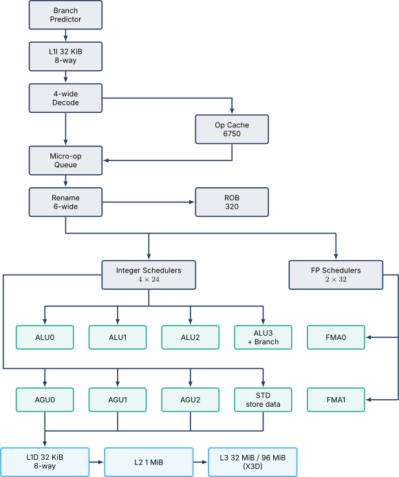
Figure 1 sketches the Zen 4 pipeline at a structural level. The figure intentionally uses the same graphical vocabulary as the Intel chapter so the reader can overlay the two diagrams to spot the architectural deltas.
02.Frontend
The Zen 4 frontend is, like Golden Cove’s, a fetch-decode-and- cache pipeline that delivers up to six micro-ops per cycle to the rename stage. The internal organization differs from Intel’s in two visible ways. First, Zen 4 keeps a 4-wide legacy decoder where Golden Cove went to 6-wide. Second, Zen 4 delivers six micro-ops per cycle from the op cache, exceeding the legacy decode width.
Branch Prediction
The Zen 4 branch predictor is the structural descendant of the Zen 3 predictor, with the tables grown roughly 50% on AMD’s public claim. The predictor is a TAGE-style direction predictor (Chapter 56) with an indirect-branch target predictor and a return address stack of 32 entries. The branch target buffer is documented in HotChips 34 as a two-level structure with a small first-level (about 1500 entries) and a larger second-level (about 7000 entries).
The misprediction recovery penalty depends on where in the pipeline the misprediction is caught. For an op-cache hit path, the recovery is 11 to 12 cycles. For a legacy-decode path, it is closer to 19 cycles. The reduced minimum recovery (compared to Golden Cove’s 17 cycles) is one of AMD’s published points of differentiation.
The predictor also runs ahead of fetch, attempting to predict the next several branch outcomes before the L1I read returns. This "lookahead" enables the prefetch of multiple sequential fetch blocks across branches, growing the effective fetch window without growing the L1I read port.
Fetch and the L1 Instruction Cache
The L1I is 32 KiB, 8-way set associative, with a 64-byte line. The capacity has not changed since Zen 1. The fetch bandwidth is 32 bytes per cycle to the predecoder. The instruction TLB is 64 entries for 4 KiB pages and 32 entries for 2 MiB pages.
The 32 KiB L1I is structurally smaller than Redwood Cove’s client-variant 64 KiB L1I (but matches Golden Cove’s 32 KiB). The implication for instruction footprint is workload-dependent. For server workloads where the instruction working set typically fits well under 32 KiB, the size is adequate. For client workloads with very large code footprints (web browsers, Electron applications), the smaller L1I shows up as a higher L1I miss rate.
Decode and the Op Cache
The Zen 4 legacy decoder is 4-wide. The four parallel decoder slots handle up to four x86-64 instructions per cycle. The slot mix is a single complex decoder and three simple decoders, by the same logic Golden Cove uses, though the Zen 4 complex decoder is documented as more capable on certain microcoded instructions.
The op cache holds approximately 6750 micro-ops and delivers six per cycle to the micro-op queue. The capacity is larger than Golden Cove’s roughly 4000 entries, but the delivery rate is lower. Golden Cove delivers 8 micro-ops per cycle from its micro-op cache and Redwood Cove between 9 and 10, against Zen 4’s 6. The combination of a wider op cache and a narrower legacy decoder is the visible manifestation of AMD’s bet that the op-cache hit rate is the dominant frontend factor for sustained throughput.
Macro-op fusion combines a compare-and-branch pair into a single fused op. Move elimination and zero-idiom recognition operate at the rename stage and do not consume op-cache space.
03.Rename and Dispatch
The Zen 4 rename engine is 6-wide. Per cycle, up to six micro-ops are renamed and dispatched. The integer PRF is 224 entries, the vector PRF is 192 entries. Both are smaller than Golden Cove’s 280 and 332 respectively, consistent with Zen 4’s smaller ROB.
The ROB is 320 entries on Zen 4, up from 256 on Zen 3 and well below Golden Cove’s 512. The smaller ROB is one of the clearest structural differences between the two designs. Combined with the narrower legacy decoder and the smaller PRFs, Zen 4 holds a smaller out-of-order window than Golden Cove at the same dispatch width.
The trade-off is power and area. A 320-entry ROB consumes substantially less area than a 512-entry ROB at the same technology node. AMD’s published power claims for Zen 4 on TSMC N5 reflect this design choice: the per-core area is smaller, the per-core power is lower at iso-frequency, but the peak single-threaded IPC on a deep workload runs a few percent behind Golden Cove.
The dispatch stage writes the renamed micro-op into the ROB and into the integer or floating-point schedulers. Zen 4 has separate schedulers for integer and FP, in contrast to Golden Cove’s unified issue queue. The integer side has four schedulers of 24 entries each (96 total entries). The FP side has two schedulers of 32 entries each (64 total entries). The total scheduler capacity is 160 entries, below Golden Cove’s 192.
04.Backend Execution Pipes
The Zen 4 backend exposes 10 dispatch pipes: four integer ALU pipes, three AGU pipes, two FMA pipes, and a separate store-data pipe. The exact distribution is documented in the Software Optimization Guide [1].
Table 1. Zen 4 execution pipes. Source: AMD Software Optimization Guide� .
| Pipe | Functional units | Notes |
|---|---|---|
| ALU0 | integer ALU | general-purpose |
| ALU1 | integer ALU, multiply | integer multiply pipe |
| ALU2 | integer ALU | general-purpose |
| ALU3 | integer ALU, branch | primary branch dispatch |
| AGU0 | load | 32 B/cycle |
| AGU1 | load | 32 B/cycle, total 2 loads/cycle to L1D |
| AGU2 | store-AGU | store address generation |
| FMA0 | FP FMA, vector | 256-bit native |
| FMA1 | FP FMA, vector | 256-bit native |
| STD | store data | writes value to STD pipeline |
The peak integer issue width is four ALU operations per cycle (one per ALU pipe). The peak load bandwidth is two loads per cycle through AGU0 and AGU1 to the L1D, totaling 64 bytes per cycle. The peak store bandwidth is one store-address generation per cycle through AGU2 plus the store-data pipe.
For floating-point and vector work, the two FMA pipes (FMA0 and FMA1) are each 256 bits wide. A single Zen 4 core can sustain two 256-bit FMA operations per cycle, equal to 16 double- precision FP operations per cycle. When running an AVX-512 instruction, the 512-bit operand is double-pumped across both FMA pipes over two consecutive cycles, sustaining 16 double-precision operations per cycle on AVX-512 code as well. The peak FLOP rate is half of Golden Cove’s full-width 512-bit configuration.
AVX-512 Without Doubling the Width
Zen 4’s AVX-512 strategy is the engineering choice with the largest visible trade-off. The full ISA is supported, including the masked and merge-masked forms, the 32 architectural 512-bit registers, the 8 mask registers, and the new AVX-512 instructions not present in AVX or AVX-2. The microarchitectural realization runs each 512-bit operation as two 256-bit operations on the FMA0 and FMA1 pipes over two cycles.
The choice has three consequences. The die area cost is substantially lower than a native 512-bit implementation. The single-instruction throughput on dense FMA AVX-512 code is half of Golden Cove’s. The mixed-workload behavior is more graceful: Zen 4 does not require the AVX-512 frequency step-down that Intel parts apply, because the per-cycle dynamic energy of two 256-bit operations is roughly the same as a single 512-bit operation. AMD’s marketing leaned heavily on this last point in the Zen 4 launch.
05.Memory Pipeline
The Zen 4 memory pipeline comprises the L1D, the L2, the L3 shared across the CCD, the load-store queues, and the prefetcher mix.
The L1D is 32 KiB, 8-way set associative, with a 64-byte line. The capacity has not changed since Zen 1, in contrast to Golden Cove’s grown 48 KiB L1D. The 8-way associativity is matched by 64 sets times 8 ways times 64 bytes per line equals 32 KiB exactly. The L1D supports two 32-byte loads per cycle, 64 bytes per cycle total.
The L2 grew from 512 KiB on Zen 3 to 1 MiB on Zen 4. The L2 hit latency is 14 cycles, up from 12 cycles on Zen 3. The doubling of capacity at modest latency cost is one of the largest visible Zen-3-to-Zen-4 improvements. The L2 prefetcher is a stream prefetcher and an IP-stride prefetcher, similar in shape to Golden Cove’s.
The L3 is 32 MiB per CCD on baseline parts and 96 MiB per CCD on X3D parts (32 MiB base plus 64 MiB stacked). The L3 hit latency is 50 cycles on baseline parts and 4 to 5 cycles longer on X3D parts due to the path through the stacked die. The L3 is a victim cache filled by L2 evictions and non-inclusive of the L2 by AMD’s documentation [1], a different organization from Intel’s NINE L3 on Sapphire Rapids.
The load queue holds 136 entries on Zen 4, up from 72 on Zen 3. The store queue holds 64 entries. Both are below the Golden Cove counterparts (192 and 114 respectively). The smaller load queue reflects the smaller ROB.
06.Chiplet Packaging and the IOD
The Zen 4 packaging strategy is the most visible microarchitectural-adjacent design choice. A single Ryzen 7000 desktop part comprises one or two CCDs and an IOD. A single EPYC 9004 server part comprises up to twelve CCDs and an IOD. The CCDs and IOD communicate over the Infinity Fabric On-Package (IFOP) link, an SerDes interconnect that crosses the substrate between dies.
The latency penalty of crossing the IFOP from a CCD to the IOD is documented as roughly 40 cycles on top of the in-CCD L3 hit latency. For a workload whose working set fits in a single CCD’s 32 MiB L3, the IFOP latency rarely matters. For a workload that crosses CCD boundaries (memory accesses to lines homed in another CCD’s L3 slice), the latency penalty is significant.
Figure 2 sketches the Genoa server packaging at a high level.
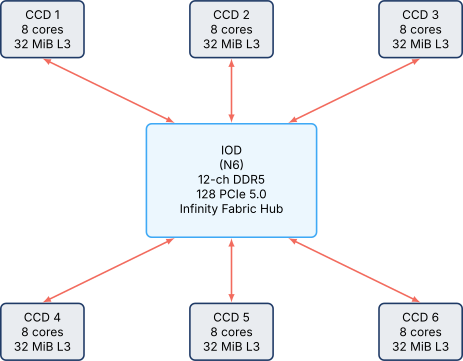
The chapter does not unpack the chiplet topology beyond this sketch. Multi-die packaging is a topic in its own right that this book does not cover. The key takeaway here is that Zen 4 trades a small inter-CCD latency cost for the ability to ship up to 96 cores per socket (twelve CCDs times eight cores) without scaling a monolithic die. Intel’s competing strategy on Sapphire Rapids uses four compute tiles connected via EMIB bridges, a different realization of the same chiplet idea.
07.3D V-Cache
The 3D V-Cache variant of Zen 4 is the most striking productized application of die stacking. A 64 MiB SRAM die is stacked directly on top of the CCD using copper-to-copper hybrid bonding (TSMC’s Stacked SoIC technology). The stacked die extends the shared L3 from 32 MiB to 96 MiB per CCD.
The latency penalty of accessing the stacked layer is 4 to 5 cycles, documented in the Genoa-X launch materials. The bandwidth between the base L3 and the stacked L3 is sustained at the on-die L3 bandwidth, with the bonding pads dense enough that the inter-die link is not a bottleneck.
Workloads that benefit most are those with a working set between 32 MiB and 96 MiB. Below 32 MiB, the base L3 captures everything. Above 96 MiB, even the stacked cache misses. In the sweet spot, the V-Cache part delivers measurable speedup over the baseline. Published benchmark results from AMD and from third-party reviewers show roughly 10% to 30% speedup on benchmark workloads in the sweet spot.
08.Zen 4 versus Zen 3
The IPC claim of approximately 13% (Zen 4 over Zen 3 at iso-frequency) breaks down into roughly four contributors, according to AMD’s HotChips 34 disclosure.
The larger op cache and the wider micro-op queue contribute several percent through reduced front-end stalls. The op-cache hit rate on a typical mix of SPEC workloads improves from roughly 75% on Zen 3 to roughly 80% on Zen 4 according to AMD’s analysis.
The larger L2 (1 MiB versus 512 KiB) contributes several percent through reduced L2 miss rate. The 2-cycle latency increase is absorbed within the larger working-set advantage. AMD’s characterization shows the L2 miss rate dropping by roughly 30% on memory-intensive benchmarks.
The larger ROB (320 versus 256) contributes several percent through deeper out-of-order look-ahead. The improvement is most visible on workloads with moderate cache miss rates, where the deeper window covers more miss latency.
The branch-prediction improvements contribute one to two percent through reduced misprediction rate and reduced minimum recovery cycles.
The full 13% breakdown is the sum of these contributions, geometrically weighted across the SPEC benchmark suite. The contribution of each factor varies by workload.
Table 2. Selected Zen 4 versus Zen 3 parameter comparison. Source: AMD Software Optimization Guide� .
| Parameter | Zen 3 | Zen 4 |
|---|---|---|
| Decode width | 4 | 4 |
| Op cache delivery | 6 per cycle | 6 per cycle |
| Op cache capacity | 4096 | 6750 |
| ROB entries | 256 | 320 |
| Integer PRF | 192 | 224 |
| Vector PRF | 160 | 192 |
| Integer scheduler total | 96 | 96 |
| FP scheduler total | 64 | 64 |
| Load queue | 72 | 136 |
| Store queue | 64 | 64 |
| L1I capacity | 32 KiB | 32 KiB |
| L1D capacity | 32 KiB | 32 KiB |
| L2 capacity | 512 KiB | 1 MiB |
| L2 hit latency | 12 cycles | 14 cycles |
| L3 capacity per CCD | 32 MiB | 32 MiB (96 X3D) |
| AVX-512 support | no | yes (double-pumped) |
| Process node | TSMC N7 | TSMC N5 |
09.Comparison with Golden Cove
Side by side, Zen 4 and Golden Cove make different trade-offs at similar peak retirement throughput. The headline differences are summarized below.
Frontend width. Golden Cove decodes 6 instructions per cycle, Zen 4 decodes 4. Golden Cove delivers 8 micro-ops per cycle from its micro-op cache, Zen 4 delivers 6.
Out-of-order window. Golden Cove holds 512 ROB entries, Zen 4 holds 320. Golden Cove holds 192 issue queue entries, Zen 4 holds 160 total scheduler entries.
Vector width. Golden Cove on server parts has native 512-bit FMA pipelines. Zen 4 has 256-bit pipelines double-pumped for AVX-512. Peak AVX-512 FLOP rate per core is roughly double on Golden Cove server parts.
L2 capacity. Golden Cove client has 1.25 MiB. Sapphire Rapids server has 2 MiB. Zen 4 has 1 MiB.
L3 organization. Golden Cove has a non-inclusive non-exclusive L3 shared across the entire die. Zen 4 has a victim-cache L3, non-inclusive of the L2, shared within a CCD, with cross-CCD accesses crossing the Infinity Fabric.
Packaging. Golden Cove on Sapphire Rapids uses four compute tiles connected via EMIB. Zen 4 on Genoa uses up to twelve CCDs arranged around a central IOD over Infinity Fabric.
The two designs converge on similar achieved IPC on most SPEC workloads. Golden Cove is faster on AVX-512-dense workloads. Zen 4 is more power-efficient at iso-throughput on most mixes, reflecting the smaller out-of-order window and the more compact vector pipelines. The V-Cache variant of Zen 4 dominates on cache-sensitive workloads with working sets between 32 MiB and 96 MiB. Neither design is uniformly better. The trade-offs between them are visible in benchmark comparisons across the two product families.
10.Worked Examples
11.Exercises
References
- [1](2024). “AMD64.”