Vector Microarchitecture
September 13, 202620 min readadvanced
The vector and SIMD instruction sets introduced in Chapter 21 make a clean architectural promise: a single instruction operates on a group of elements, producing multiple results from one decode and one issue…
The vector and SIMD instruction sets introduced in Chapter 21 make a clean architectural promise: a single instruction operates on a group of elements, producing multiple results from one decode and one issue slot. The architectural model is uniform across the vector. The microarchitectural implementation is where the interesting engineering happens.
The naive implementation is a brute-force ALU that is times as wide as a scalar ALU. A 256-bit vector add on AVX-512 with 32-bit elements is 8 parallel adds, so the natural execution unit is 8 32-bit adders in parallel. The natural register file is 8 banks of single-precision registers. The natural memory port is an 8-element-wide load and store unit. This brute-force approach works at small widths but scales poorly as the vector width grows. At AVX-512’s 512 bits, the unit would be 16 32-bit ALUs in parallel, with a 512-bit-wide register file and a 512-bit memory port. At RVV’s optional 4096-bit vectors, the brute-force approach is impractical.
Real designs combine several techniques to scale vectors without proportional cost. Lanes are time-multiplexed: a 4-lane unit runs an 8-element vector in 2 cycles. Chaining forwards output elements as they become available, so back-to-back vector ops overlap. Masks let one vector instruction skip lanes for unselected elements without serializing. Scalable vectors let the microarchitecture pick its own lane count and run any vector length the ISA permits.
This chapter develops vector microarchitecture from first principles. It starts with the lane organization and time- multiplexed execution, develops the vector register file, covers masking and predication, treats gather/scatter implementation, develops chaining for back-to-back vector ops, and closes with the scalable-vector approach in ARM SVE and RISC-V V (RVV) as contrasted with the fixed-length AVX-512 and NEON.
01.Lane Organization and Time Multiplexing
A vector execution unit is organized as a number of parallel lanes, each lane being a complete arithmetic pipeline for one element. A 4-lane integer add unit has 4 independent 32-bit adders. On each cycle, the unit issues an add instruction (or holds the existing one), and 4 element-wise adds happen in parallel.
A concrete numerical example fixes the scale. Intel’s Sunny Cove implements AVX-512 with a 512-bit execution unit, which is 16 parallel 32-bit lanes. Each lane has its own register read port, its own ALU, and its own write port. The unit can complete one 512-bit vector add per cycle, processing 16 32-bit elements in the same cycle. The total throughput is 16 element-operations per cycle on this single unit.
AMD’s Zen 4 implements AVX-512 with a 256-bit execution unit that processes 512-bit vectors in 2 cycles. Eight lanes (instead of 16) handle the lower half on one cycle and the upper half on the next. The architectural latency of an AVX-512 add on Zen 4 is therefore 2 cycles for a 512-bit operation, compared to 1 cycle on Sunny Cove. The throughput is half the lane count.
The time-multiplexing pattern generalizes. A 4-lane unit processing an 8-element vector runs in 2 cycles. A 4-lane unit processing a 16-element vector runs in 4 cycles. The instruction is the same, the unit is the same, the latency is the vector length divided by the lane count, rounded up.
The lane count is a design choice that trades silicon area for throughput. Doubling the lane count doubles the throughput but also doubles the area, the power, and the register file ports. Modern high-end CPUs (Intel Sunny Cove, AMD Zen 4, ARM Neoverse V2) carry 8 to 16 lanes of single-precision floating-point in the vector unit. GPUs carry hundreds to thousands of lanes per SM, organized differently because of the SIMT execution model.
02.The Vector Register File
The vector register file (VRF) is sized differently from the scalar register file. AArch64 NEON has 32 vector registers, each 128 bits, for 512 bytes of architectural state. AArch64 SVE extends this to 32 registers of 128 to 2048 bits each (the actual width is implementation-specific), so the architectural state is 512 bytes to 8 KiB.
AVX-512 has 32 registers (in 64-bit mode), each 512 bits, for 2 KiB of architectural state. RVV has 32 vector registers of implementation-specific width (128 to 1024 bits on current designs, with the spec allowing up to 65,536 bits, or 8 KiB).
The physical register file is larger than the architectural file to support renaming and out-of-order execution. Modern x86-64 cores carry physical vector register files in the 200 to 400 entry range, sized to match the ROB and issue queue capacity. At 512 bits per entry that is 12 to 25 KiB of vector register file, larger than the scalar register file by a factor of 5 to 10.
Multi-Bank Organization
A vector register file with 16 lanes and a 2-port-read-1-port- write per lane requires 32 read ports and 16 write ports total. A single-bank SRAM with that many ports is impractical. The solution is to bank the register file. A common organization is one bank per lane: lane 0 holds element 0 of every vector register in its own SRAM, lane 1 holds element 1, and so on.
With banking, each lane needs only the read and write ports for its single-element data, which is feasible. The register address generation broadcasts the same register name to all lanes, and each lane reads its own element from its own bank. The output of each lane goes to that lane’s ALU, and the ALU result writes back to that lane’s bank.
The banking constrains the operations the unit can do efficiently. A within-lane operation (vector add, vector multiply, vector load/store of contiguous elements) is fast because each lane works independently. A cross-lane operation (vector reduction, shuffle, permute, gather/scatter) is slower because lanes must exchange data through a separate network.
03.Masking and Predication
A vector instruction operates on all elements of the vector register. If only some elements need processing (the remaining elements should be left unchanged), the program could in principle use scalar code, but that defeats the throughput advantage. Vector ISAs provide masks (also called vector predicates) that mark which elements are active on a per-instruction basis.
A mask is a vector of bits, one bit per element of the data vector. A 16-element data vector has a 16-bit mask. When the vector instruction executes, lanes whose mask bit is 1 perform the operation, and lanes whose mask bit is 0 leave their destination element unchanged (or, in some ISAs, set to zero, depending on the masking mode).
AVX-512 uses dedicated 64-bit mask registers k0 through k7. SVE uses 16 predicate registers p0 through p15, each holding one predicate bit per byte of the vector. RVV takes its mask from v0, where bit of v0 controls element .
The microarchitectural implementation of masking has two flavors. The simple version executes the full vector operation in all lanes, then conditionally writes back the result based on the mask. All lanes burn power. The energy-saving version uses the mask to clock-gate the unselected lanes, so they do not burn power. The energy version requires more lane-local control logic but is preferred in modern designs.
Masking is more efficient than the if-conversion equivalent in scalar code. A scalar conditional add takes one cycle for the branch (assuming no misprediction) and one cycle for the add. A masked vector add does both in one vector instruction, with the branch removed entirely. The instruction count drops, the branch predictor sees no entropy, and the IPC ceiling rises.
04.Gather and Scatter
Gather and scatter let a vector load or store operate on non-contiguous memory locations. A gather takes a vector of indices and loads each element from a different address. A scatter does the same in reverse for stores.
The canonical pattern is the indexed access in scientific code: y[i] = x[index[i]]. Without gather, the compiler emits a loop with one scalar load per element. With gather, the compiler emits one vector load that processes 8 or 16 indices in one instruction.
The microarchitectural implementation is much harder than contiguous loads. A contiguous vector load fetches a single cache line (or two if the access crosses a line boundary) and extracts the elements. A gather fetches potentially different cache lines, one per element. Each cache lookup is a separate operation, and the line addresses are not known until the index vector is computed.
Modern AVX-512 gather instructions (vgatherdpd, vgatherdps) take 16 cycles on Sunny Cove for a 16- element gather (one element per cycle through the L1 port), and more if any element misses the cache. AMD’s Zen 4 gather is similar in throughput, with some refinements. ARM SVE’s ld1d gather is similarly bottlenecked by the load port count.
Optimizations for Locality
Modern implementations of gather detect when consecutive indices land in the same cache line and coalesce them into a single cache access. A gather with 16 indices that all fall in the same 64-byte line completes in one cache access, not 16. The hardware identifies the locality by comparing the index addresses at the cache-line granularity (top 58 bits) and merging matching ones.
The savings are large when the indices are correlated. A strided access pattern with stride 8 bytes (loading every 8-byte element from an aligned array) has 8 indices in each 64-byte line, so a 16-element gather hits 2 lines and completes in 2 cache accesses. The hardware coalescing turns a worst-case 16- cycle operation into a 2-cycle operation. Packing the elements more densely helps further, and 16 contiguous 4-byte elements from an aligned array fill exactly one 64-byte line and complete in a single access.
05.Chaining
A vector unit running a single instruction at a time is wasteful. Two consecutive vector instructions could overlap their execution: the first instruction’s lane-1 result can feed the second instruction’s lane-1 input before lane-2 of the first is even finished. The mechanism that enables this overlap is chaining.
In a chained pipeline, each lane operates independently. As soon as lane of instruction A finishes, lane of instruction B can start (assuming the two are dependent through that lane). The total time for both instructions is the time for the longer one, plus a per-lane forwarding cost, not the sum of the two times.
A worked example fixes the picture. Suppose the vector unit has 4 lanes and the vector length is 16, so each instruction takes 4 cycles to process all 16 elements. Without chaining, two instructions take cycles. With chaining, lane 1 of instruction B starts as soon as lane 1 of instruction A finishes (at cycle 1), and the unit processes both instructions in overlapping phases. The total cycles are , where the extra 1 is the pipeline depth of one lane’s ALU.
Chaining is the vector analog of operand forwarding in scalar pipelines (Chapter 29). The historical name comes from the Cray-1 supercomputer, which implemented chaining in 1976 and demonstrated the dramatic throughput improvement it provides on vector code.
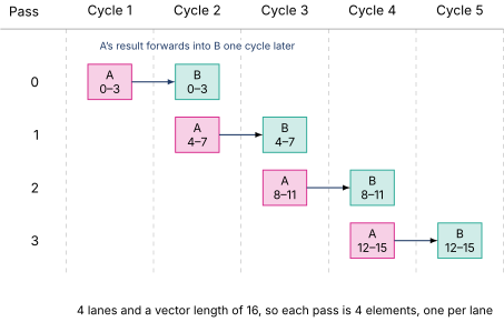
Modern AVX-512 and SVE implementations chain back-to-back vector ops on the same execution port. The chaining is transparent to the programmer. The performance counters expose the effective throughput, which on dependent chains is close to the per-cycle ALU latency rather than the per-vector latency.
06.Scalable Vectors: SVE and RVV
The vector ISAs covered so far (NEON at 128 bits, AVX-512 at 512 bits) fix the vector length in the ISA encoding. Code compiled for AVX-512 assumes 512-bit vectors. Code compiled for NEON assumes 128-bit vectors. The fixed-length design simplifies the compiler (the compiler knows the vector length and can unroll accordingly) but ties the code to a specific microarchitecture generation.
ARM’s Scalable Vector Extension (SVE) [1] and RISC-V’s Vector extension (RVV) [2] take a different approach. The vector length is an implementation property of the hardware, not the ISA. Programs are written in a length-independent style. Each vector instruction processes "whatever the hardware can do" in one shot, and a separate query mechanism tells software how many elements were actually processed.
SVE Programming Model
An SVE vector register is between 128 and 2048 bits, in 128-bit increments. The actual width is reported by the hardware to software via the cntb instruction (count bytes per vector). Programs use predicate-controlled loops to process arrays of any size:
SVE length-independent loop
| mov x0, #0 // i = 0 | |
| whilelt p0.s, x0, x1 // mask for i to N (saturating) | |
| loop: | |
| ld1w z0.s, p0/z, [x2, x0, lsl #2] // load x[i:i+VL] | |
| ld1w z1.s, p0/z, [x3, x0, lsl #2] // load y[i:i+VL] | |
| fmla z1.s, p0/m, z0.s, z2.s // y[i:i+VL] += x[i:i+VL] * scalar | |
| st1w z1.s, p0, [x3, x0, lsl #2] // store y[i:i+VL] | |
| incw x0 // i += VL | |
| whilelt p0.s, x0, x1 // update mask for next iteration | |
| b.first loop // continue if any elements remain |
The same code runs on a 128-bit SVE implementation (processing 4 single-precision elements per iteration) and on a 2048-bit SVE implementation (processing 64 elements per iteration). The whilelt instruction generates a predicate covering only the remaining elements, so the final iteration of the loop processes the partial-width tail naturally.
RVV Programming Model
RVV is similar but uses a different mechanism. The program sets the vector length explicitly via the vsetvli instruction, which takes the requested number of elements and the data type, and returns the actual number of elements the hardware will process this iteration. The program then issues vector instructions that process that number of elements.
RVV length-independent loop
| loop: | |
| vsetvli t0, a0, e32, m1 # request VL elements of 32-bit type | |
| vle32.v v0, (a1) # load v0 = x[i:i+VL] | |
| vfmul.vf v1, v0, fa0 # v1 = v0 * scalar | |
| vse32.v v1, (a2) # store y[i:i+VL] = v1 | |
| slli t1, t0, 2 # bytes processed = VL * 4 | |
| add a1, a1, t1 | |
| add a2, a2, t1 | |
| sub a0, a0, t0 # remaining = remaining - VL | |
| bnez a0, loop |
The vsetvli instruction lets the hardware set the effective vector length per iteration. A 1024-bit RVV implementation may set VL = 32 single-precision elements, while a 128-bit implementation sets VL = 4. The program’s source code is identical.
Microarchitectural Implications
The scalable design constrains the hardware in interesting ways. The vector length is an implementation property, so the hardware designer can choose the lane count, the register file width, and the memory port width independently. A high-end implementation can be 1024 bits wide. A low-end implementation can be 128 bits wide. Both run the same binary.
The cost is in the masking and predication infrastructure. SVE and RVV use predicate-controlled loops as the main control mechanism, which means every vector instruction reads a mask register in addition to its data inputs. The mask register file is an extra structure that fixed-length ISAs (NEON, AVX-512) do not need to use as heavily.
A second cost is reduction and permute operations, which need to know the actual VL to operate correctly. A fixed-length ISA hard-codes the VL into the reduction tree, so a 16-element sum is a 4-level tree of 8, 4, 2, and 1 adders. A scalable-length ISA needs the tree to handle any VL up to the maximum, which often means a sequential reduction loop instead of a flat tree.
Table 1. Vector ISA comparison
| ISA | Fixed / Scalable | Width range | Mask register |
|---|---|---|---|
| NEON | Fixed | 128 bits | none (uses data) |
| AVX-512 | Fixed | 512 bits | k0–k7 (64 bits each) |
| SVE | Scalable | 128–2048 bits | p0–p15 (per-byte) |
| RVV | Scalable | 128 bits–8 KiB | v0 (bit per element) |
07.Putting It Together
A modern high-end CPU’s vector microarchitecture combines all the elements above. The execution unit has 8 to 16 lanes, chained for back-to-back operations. The register file is banked per lane and renamed through the same renamer that handles scalar registers (Chapter 51). Masks are stored in dedicated mask registers (AVX-512) or in vector registers (RVV) and applied at issue time. Gather and scatter operate through the same load-store unit covered in Chapter 54, with coalescing logic to combine same-cache-line accesses.
The relationship between vector throughput and scalar IPC is additive. A core that retires 4 scalar instructions per cycle and also retires 1 vector instruction per cycle (with each vector instruction processing 16 elements) has a peak throughput of element-operations per cycle. Vectorization is therefore one of the largest IPC multipliers available to a compiler, and the microarchitecture is sized to support it.
The vector unit is also a substantial fraction of the core area. On modern x86-64 cores, the AVX-512 unit (lane logic, register file, mask handling, gather/scatter) accounts for 20 to 30 percent of the core area. On ARM Neoverse V2 the SVE unit is similar. The investment is large enough that vendors have at times shipped cores with the vector unit fused off (e.g., Intel’s early Alder Lake E-cores had no AVX-512) to recover the area on workloads that did not use it.
08.Worked Examples
09.Exercises
References
- [1]Stephens, Nigel and Biles, Stuart and Boettcher, Matthias and Eapen, Jacob and Eyole, Mbou and Gabrielli, Giacomo and Horsnell, Matt and Magklis, Grigorios and Martinez, Alejandro and Premillieu, Nathanael and Reid, Alastair and Rico, Alejandro and Walker, Paul (2017). “The ARM Scalable Vector Extension.” In IEEE Micro, Vol. 37, No. 2, pp. 26--39. doi:10.1109/MM.2017.35
- [2]RISC-V International (2021). “RISC-V ``V''.”
- [3](2024). “ARM.”
- [4](2024). “Intel.”
- [5](2024). “AMD64.”