The Classic 5-Stage Pipeline (IF-ID-EX-MEM-WB)
September 8, 202630 min readintermediate
The previous chapter introduced pipelining as an idea, the equivalent of an assembly line for instructions. This chapter builds the canonical design that almost every introductory architecture text treats as…
The previous chapter introduced pipelining as an idea, the equivalent of an assembly line for instructions. This chapter builds the canonical design that almost every introductory architecture text treats as the reference point. Five stages, four pipeline registers, one new instruction launched every cycle in steady state. The design is the RV32I 5-stage pipeline that traces its lineage to the MIPS R2000 of 1986 and that still serves today as the teaching vehicle for in-order processor design.
The chapter is descriptive rather than analytical. It walks through each of the five stages, naming every wire and every control signal. It then catalogs the four pipeline registers and the exact fields each one carries. Hazards (the situations that keep the pipeline from delivering one instruction per cycle) are the subject of Chapter 30. The intent here is to fix the structural picture before complicating it.
A reader who has worked through the single-cycle datapath of Chapter 25 and the multi-cycle datapath of Chapter 27 will recognize most of the parts. The arithmetic-logic unit, the register file, the data memory, the sign extender, and the branch comparator are unchanged. What changes is how they are wired together and which signal lives in which clock cycle. The cover of this book carries a schematic of exactly the datapath described in this chapter, with the five stages drawn left to right and the four pipeline registers as vertical amber bars between them. Refer to it when the prose descriptions of signal routing become hard to track.
01.The Picture Before the Pieces
Five stages execute concurrently. At any instant in steady state, five different instructions are in flight, one per stage. The program counter is producing the address of instruction in IF while the instruction-decode stage finishes pulling instruction apart. The ALU in EX is computing the result of instruction . The data memory in MEM is reading or writing for instruction . The register file in WB is committing the result of instruction to its destination register.
Figure 1 lays those five stages out against time, one row per instruction and one column per cycle. The diagonal is the pipeline filling. The shaded column is the instant described above, with all five stages busy on five different instructions.
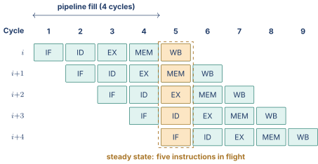
Imagine four hundred RV32I instructions running on the 5-stage pipeline at a clock of GHz. The first instruction enters IF at cycle 1 and leaves WB at the end of cycle 5. The second enters IF at cycle 2 and leaves WB at cycle 6. By the time the last instruction leaves WB, cycles have elapsed, not the that the same five steps would take if each instruction ran to completion before the next one started. The four-cycle startup overhead is what the literature calls the pipeline fill, and it disappears into the noise as soon as the instruction count grows past a few tens.
The single-cycle design from Chapter 25 runs the same four hundred instructions in 400 cycles at a clock that has to accommodate the worst-case datapath delay, which is the load path through I-memory, register read, ALU, D-memory, and register writeback. The multi-cycle design from Chapter 27 ran each instruction in three to five faster cycles but never overlapped them. The 5-stage pipeline is the first design that simultaneously gets a fast clock and one-instruction-per-cycle throughput.
02.Instruction Fetch (IF)
The IF stage has three jobs in one cycle. It reads the current program counter. It addresses the instruction memory with that PC and captures the returned instruction. It computes for the next sequential instruction. The fetched instruction word, the PC that fetched it, and are all written into the IF/ID pipeline register at the rising clock edge that ends the cycle.
The PC Register and the Next-PC Mux
The program counter is a 32-bit edge-triggered register. Its input is driven by a 2-to-1 multiplexer (in the simplest design) that selects between and a branch target address computed downstream. When no branch is in flight, the mux selects and the program advances one instruction at a time. When a branch in EX evaluates true, the mux selects the branch target, and the PC jumps.
In a 32-bit RISC-V implementation the constant 4 reflects the fact that every base-ISA instruction is four bytes. A compressed-ISA implementation that also supports the C extension would compute either or depending on whether the fetched halfword indicates a compressed or a full instruction. This chapter sticks to plain RV32I.
The Instruction Memory Port
The instruction memory is treated, in this idealized model, as a single-cycle asynchronous (combinational) read port. The PC value drives the address lines at the beginning of the cycle. By the end of the same cycle, the instruction word at that address is available on the data lines. Real processors do not have this luxury, because DRAM and even on-chip SRAM caches take multiple cycles. Filling that gap is the responsibility of the instruction cache, covered in Part IV of this book.
The PC Adder
A small 32-bit adder runs in parallel with the instruction-memory access. It computes and feeds that value to two destinations. First, to the next-PC mux as the default next value. Second, to the IF/ID register so that downstream stages can use as the return address saved by JAL and JALR. The PC itself travels down IF/ID alongside it, because the branch-target adder in EX needs the instruction’s own address rather than the incremented one.
03.Instruction Decode (ID)
The ID stage receives the 32-bit instruction word from IF/ID and extracts every field that any later stage might need. In practice this means three concurrent activities. The first is register read, which presents the rs1 and rs2 fields of the instruction to the register file and captures the two read values. The second is immediate generation, which sign-extends the appropriately-scattered immediate bits into a 32-bit value. The third is control- signal decode, which translates the opcode and function fields into the control signals that the EX, MEM, and WB stages need.
Reading the Register File
The RV32I register file has 32 entries of 32 bits each, two read ports, and one write port. The two read ports are combinational in the canonical design: the address lines arrive at the start of the cycle, and the read data appears within the same cycle. The write port is synchronous and is driven by the WB stage on the falling half of the same clock or, equivalently, by the preceding rising edge. Many implementations clock the write port on the rising edge and rely on internal forwarding within the register file so that a write in WB is visible to a read in ID in the same cycle. Either convention works for the discussion here.
The two read addresses come directly from instruction bits [19:15] (rs1) and [24:20] (rs2). The two read data values flow into the ID/EX pipeline register. The destination field rd from bits [11:7] is captured into ID/EX as well, because the WB stage three cycles later still needs to know which register to write.
Generating the Immediate
The RV32I immediate is scattered across the instruction word in different positions depending on the instruction format. The I-format encodes a 12-bit signed immediate in bits [31:20]. The S-format puts the upper bits in [31:25] and the lower bits in [11:7]. The B-format scatters its 13-bit immediate (with the low bit implicit zero) across [31], [7], [30:25], and [11:8]. The U-format places its 20-bit upper immediate in [31:12], with the lower 12 bits of the result implicit zero. The J-format scatters its 21-bit immediate across [31], [19:12], [20], and [30:21], also with the low bit implicit zero.
The immediate generator is a small combinational block whose job is to pick the right bits, shift them into place, and sign-extend the result to 32 bits. It needs to know the instruction format, which it determines from the seven-bit opcode in bits [6:0].
Producing the Control Signals
A small block of combinational logic, the control unit, maps the opcode and function fields to the set of control signals listed in Chapter 26. The signals are partitioned according to which downstream stage uses them. EX-stage signals include the ALU operation code, the operand-B mux select (register or immediate), and the branch-comparator function. MEM-stage signals include the memory-read enable, the memory-write enable, and the access width. WB-stage signals include the writeback-mux select (ALU result or memory data) and the register-write enable. All of these flow into ID/EX, where they wait their turn.
04.Execute (EX)
The EX stage centers on the arithmetic-logic unit. The ALU takes two 32-bit operands and an operation code, and produces a 32-bit result. The first operand is the value of rs1 that came down ID/EX for every instruction that reads a source register. LUI and AUIPC are the exception, because the U-format has no rs1 field at all, and the exercises at the end of the chapter ask what the operand-A path needs in order to accommodate AUIPC. The second operand is selected by a 2-to-1 mux between the value of rs2 and the sign-extended immediate. The mux select line is one of the control signals generated in ID.
ALU Operations in RV32I
The RV32I ALU supports ten operations: ADD, SUB, AND, OR, XOR, SLL (shift-left logical), SRL (shift-right logical), SRA (shift-right arithmetic), SLT (set-less-than signed), and SLTU (set-less-than unsigned). A four-bit operation code is sufficient to select among these ten, with extra codes reserved for future use. The implementation details of each operation were treated in Chapter 7.
For arithmetic-immediate instructions (ADDI, ANDI, ORI, etc.) the ALU operation is the same as for the register-register form, and only the operand-B mux changes. For load and store instructions, the ALU performs an ADD between rs1 and the sign-extended immediate, producing the byte address used by the MEM stage. For branches the ALU is not strictly needed for the comparison itself in the canonical design (a dedicated branch comparator handles that), but many implementations route the branch comparison through the ALU’s subtract path to save area.
Branch Resolution Location
In the canonical 5-stage RISC-V design, branches resolve in EX. A dedicated branch comparator takes the rs1 and rs2 values from ID/EX and produces a single bit indicating whether the branch condition (BEQ, BNE, BLT, BGE, BLTU, BGEU) is true. A 32-bit adder in EX computes the branch target as , where the PC traveled down ID/EX and the immediate is the sign-extended B-format value.
If the branch comparator says taken, the branch-taken signal travels back to IF as a control input to the next-PC mux, and the two instructions that the IF stage already fetched (the one in ID and the one in IF itself) are squashed. The exact machinery of squashing and the cost in cycles is the subject of Chapter 30. Resolving branches in EX, two stages after fetch, means each taken branch costs two bubbles in the simplest design. Some teaching pipelines move branch resolution into ID to reduce this penalty to one bubble, at the cost of adding a comparator to the ID stage and stressing the critical path.
05.Memory Access (MEM)
The MEM stage is where load and store instructions interact with the data memory. The address comes from the ALU output that arrived through EX/MEM. The data to store (for stores) comes from the rs2 value, which has been carried alongside the address through ID/EX and EX/MEM. The control signals MemRead, MemWrite, and the access-width fields came down from ID. Like the instruction memory in IF, the data memory is modeled as a single-cycle port whose read is asynchronous (combinational) and completes within the cycle, and whose write is synchronous and commits on the clock edge that ends the cycle. The complications introduced by real caches are deferred to Part IV.
Load Path
For a load (LW, LH, LB, LHU, LBU), the address from EX/MEM drives the data-memory read port. The returned 32-bit value is then funneled through a load-extension unit that performs sign-extension or zero-extension based on the access width and signedness. The final 32-bit loaded value is captured into MEM/WB.
A byte load from address 0x1000_0003 reads 32 bits at the aligned word address 0x1000_0000 and selects the byte at position three. The load-extension unit picks that byte out, sign-extends it to 32 bits for LB, or zero-extends it for LBU.
Store Path
For a store (SW, SH, SB), the address from EX/MEM drives the address port, the data from rs2 drives the data port, and the access-width signals drive the byte-enable lines that determine which bytes of the addressed word are actually written. The MEM/WB pipeline register still captures whatever the EX/MEM ALU result was, but it is not needed for a store, since stores produce no register destination.
Non-Memory Instructions in MEM
Arithmetic and logical instructions have nothing to do in MEM. Their ALU result travels through EX/MEM to MEM/WB unchanged, and the data memory’s read and write enables are de-asserted. The stage still consumes one cycle for them, because every instruction must visit every stage in order in this simple in-order pipeline. The empty visit is the cost of uniform stage boundaries.
06.Writeback (WB)
The WB stage is the simplest. A 2-to-1 multiplexer selects between the loaded data (from MEM) and the ALU result (passed through from EX). The selected value, together with the destination register number and the register-write enable signal, drives the register file’s write port. If the register-write enable is asserted, the destination register is updated on the clock edge that ends the cycle.
The choice between load data and ALU result is determined by the MemToReg control signal, which has been traveling down the pipeline since ID. For loads it selects the load extender’s output. For arithmetic instructions, jump-and-links, LUI, and AUIPC, it selects the ALU result. For stores and branches the register-write enable is zero and the mux output is irrelevant.
07.The Pipeline Registers
The four pipeline registers are the heart of the design. Each one sits between two adjacent stages and captures every signal that the later stage will need. They are clocked on the same edge as the rest of the design (the rising edge in this book), so all four registers latch simultaneously. The contents of stage at cycle become available to stage at cycle .
The exact field list per register is determined entirely by which downstream stages consume which signals. A signal that EX uses is captured in ID/EX. A signal that MEM uses is captured in ID/EX and then in EX/MEM. A signal that WB uses is captured in ID/EX, then EX/MEM, then MEM/WB. Control signals propagate this way, which is why a register-write enable that is generated in ID at cycle does not actually drive the register file until cycle .
IF/ID
IF/ID carries three things: the 32-bit instruction word fetched this cycle, the PC of that instruction, and the value of . The instruction word is consumed by the decoder, by the register-file address ports, and by the immediate generator. The PC is needed by the branch target adder in EX, which adds the sign-extended immediate to the instruction’s own address. is needed by the link-write path of JAL and JALR.
ID/EX
ID/EX is the widest of the four. It carries the two register-read values, the 32-bit sign-extended immediate, the value (so the branch adder can compute the target), the value (the link address that JAL and JALR write), the rd field (so WB three cycles later knows where to write), the rs1 and rs2 fields (needed for forwarding logic in the next chapter), and the full bundle of control signals destined for EX, MEM, and WB.
EX/MEM
EX/MEM holds the ALU result, the rs2 value (in case MEM needs it as store data), the rd field for WB, the branch-taken decision from the comparator (if branches resolve in EX), the computed branch target address, and the MEM- and WB-stage control signals.
MEM/WB
MEM/WB holds the ALU result (passed through), the loaded data (if the instruction was a load), the rd field, and the WB-stage control signals (the writeback-mux select and the register-write enable).
Table 1. Pipeline register contents
| Register | Contents |
|---|---|
| IF/ID | instr[31:0], PC, |
| ID/EX | rs1_val, rs2_val, imm, PC, , rd, rs1, rs2, ctrl(EX,MEM,WB) |
| EX/MEM | ALU_result, rs2_val, rd, br_taken, br_target, ctrl(MEM,WB) |
| MEM/WB | ALU_result, mem_data, rd, ctrl(WB) |
The total width is the sum of every field in the table. A rough count for an RV32I implementation puts the pipeline-register storage at around 450 to 500 flip-flops in total. That is a small overhead compared with the 1024 flip-flops in the register file, and it is the price of admission to one-instruction-per-cycle throughput.
08.Walking an Instruction Through the Pipeline
The cleanest way to internalize the pipeline is to follow a single instruction from fetch to writeback, and then to overlay a sequence so the parallelism becomes visible.
Consider the instruction ADD x10, x11, x12 sitting at address 0x1000 in the instruction memory. In cycle the IF stage drives 0x1000 into the I-memory address port and reads back the 32-bit encoding. The PC adder produces 0x1004 in parallel. At the clock edge ending cycle , the instruction word, the address 0x1000, and 0x1004 are latched into IF/ID.
In cycle the ID stage pulls rs1 and rs2 out of the instruction word. The register file returns the values of x11 and x12 during the same cycle. The immediate generator produces a value that the EX stage will ignore (because the operand-B mux will pick rs2). The control unit decodes the opcode and produces the ALU-operation code for ADD, operand-B-mux select set to register, all memory enables off, writeback-mux set to ALU result, and register-write enable on. Everything latches into ID/EX at the clock edge.
In cycle the ALU adds the two operand values, producing the sum. EX/MEM latches the result, the destination register number , and the surviving control signals (memory enables off, write-back-mux for ALU result, register-write enable on).
In cycle the MEM stage does nothing useful for this instruction. The ALU result passes through. MEM/WB latches the ALU result and the writeback control signals.
In cycle the WB stage selects the ALU result (because MemToReg is zero), drives it onto the register file write-data port together with and write-enable on. At the end of cycle the register file commits the sum into x10.
Five cycles, one instruction, no overlap. Now consider three consecutive instructions starting at the same address:
Three instructions in flight
| 0x1000: ADD x10, x11, x12 ; rs1=x11, rs2=x12, rd=x10 | |
| 0x1004: SUB x13, x14, x15 ; rs1=x14, rs2=x15, rd=x13 | |
| 0x1008: AND x16, x17, x18 ; rs1=x17, rs2=x18, rd=x16 |
The first instruction enters IF at cycle 1. At cycle 2 it is in ID and the second instruction is in IF. At cycle 3 the first is in EX, the second in ID, and the third in IF. At cycle 4 the first is in MEM, the second in EX, the third in ID, and a fourth (the next instruction at 0x100C) has entered IF. At cycle 5 every stage is occupied, the first instruction is in WB, and the steady-state cadence of one writeback per cycle has begun.
Table 2. Three-instruction pipeline diagram
| Cycle | 1 | 2 | 3 | 4 | 5 |
|---|---|---|---|---|---|
ADD x10 | IF | ID | EX | MEM | WB |
SUB x13 | IF | ID | EX | MEM | |
AND x16 | IF | ID | EX |
This diagram is the canonical pipeline picture, sometimes called a reservation table (although that term has a more specific meaning in scheduling theory). Each row is one instruction. Each column is one cycle. The cell tells which stage that instruction occupies. In steady state, every column has exactly five filled cells, one per stage.
09.Clock Period and Stage Balance
The pipeline’s clock period must accommodate the slowest single stage, plus the setup time of the pipeline register at the end of that stage, plus the clock-to-Q propagation delay of the pipeline register at the start. In the canonical 5-stage design the slowest stage is usually MEM (because the data memory is the slowest single combinational path) or EX (because the ALU’s carry propagation through 32 bits dominates).
A representative timing for a 65 nm CMOS RV32I core might allocate, for each stage:
Table 3. Sample stage delays
| Stage | Combinational delay |
|---|---|
| IF | 0.7 ns (I-memory access) |
| ID | 0.5 ns (register read + decode + imm gen) |
| EX | 0.8 ns (32-bit ALU + branch comparator) |
| MEM | 0.9 ns (D-memory access + load extension) |
| WB | 0.3 ns (writeback mux + register write setup) |
The clock period must be at least ns, where the two 0.1 ns terms are representative pipeline-register setup and clock-to-Q. The clock frequency is therefore about ns MHz. The unpipelined version of the same datapath would need a clock period of at least ns, for a clock of about MHz. The pipelined design is roughly 2.9 times faster in throughput.
Stage balance is an active design constraint. Designers move work between stages, add internal pipelining inside a long stage, or add a cycle of latency through a stage that contains a long combinational path. The next chapter takes stage balance as given and focuses on the dynamic dependencies between instructions that prevent the pipeline from running at its nominal rate even with perfect static balance.
10.Single-Cycle, Multi-Cycle, and Pipelined Compared
The three designs from this Part of the book share most of their component blocks. They differ in how those blocks are wired in time. Chapter 25 executes one instruction per cycle but pays for a slow clock. Chapter 27 spreads each instruction across three to five cycles, each of which is short, but never overlaps two instructions. The pipelined design from this chapter overlaps five instructions, one per stage, at the same fast clock as multi-cycle.
For a workload of instructions where the single-cycle clock period is , the multi-cycle clock period is , and the pipelined clock period is (very close to ):
-
Single-cycle execution time: .
-
Multi-cycle execution time: , where is the average cycles per instruction (CPI), typically between 3 and 5.
-
Pipelined execution time: in the ideal case, which for large tends to .
For typical numbers, is about three to five times , so the pipelined design wins by roughly a factor of over both alternatives once the pipeline is full. This is the bargain that makes pipelining the universal choice for general-purpose CPUs.
11.Why This Is the Reference Design
The 5-stage IF-ID-EX-MEM-WB pipeline is not the only way to build a pipelined RISC processor. Real implementations vary. The original MIPS R2000 used essentially this layout. The ARM7TDMI used a three-stage pipeline (fetch, decode, execute). The Cortex-M3 uses three stages. Modern Cortex-A series cores use 12 to 15 stages. The Intel Pentium 4 used 20 to 31 stages depending on the revision. Chapter 32 examines why deeper pipelines stopped paying off past a certain depth.
Two reasons keep the 5-stage layout as the textbook reference. First, it is the smallest pipeline that exposes all the hazard types that any longer pipeline must also handle. Structural, data, and control hazards all appear naturally in 5 stages, which makes the design pedagogically rich. Second, it maps cleanly onto the RV32I instruction set without overcrowding any single stage. Every RV32I instruction visits every stage. There are no irregular paths.
12.Worked Examples
13.Exercises
References
- [1]Patterson, David A. and Hennessy, John L. (2020). “Computer Organization and Design RISC-V Edition: The Hardware Software Interface.” Morgan Kaufmann.