The Control Unit
September 13, 202627 min readintermediate
The single-cycle datapath of Chapter 25 sits inert without a control unit. The wires are in place, the functional units are wired together, but every multiplexer select, every memory enable, and every register…
The single-cycle datapath of Chapter 25 sits inert without a control unit. The wires are in place, the functional units are wired together, but every multiplexer select, every memory enable, and every register write needs a signal that says “on” or “off” at the right moment. The control unit is the block that decides what each instruction means and translates that meaning into the bit pattern of control signals that the datapath needs.
This chapter builds the control unit two ways. The first is hardwired, the dominant style in RISC processors and in every RV32I implementation. A purely combinational decoder reads the instruction’s opcode and function fields and emits the control signal vector for that instruction. The second is microcoded, the dominant style in early CISC processors and still present in modern x86. A small ROM holds a program (the microcode) that sequences each architectural instruction through one or more cycles of control signal vectors. Both styles are still in use, in different roles, in 2026. The chapter develops the truth table for the single-cycle RV32I control unit, traces the historical origin of microcode to Wilkes in 1951 [1], and explains why RISC-V uses hardwired control while modern x86 retains microcode for the most complex instructions.
01.What the Control Unit Must Decide
The complete single-cycle datapath of [fig:complete-datapath] contains roughly ten control signals. For each instruction class, the control unit must produce the correct value of each signal.
The signal inventory
Table 1. The control signals of the single-cycle RV32I datapath.
| Signal | Width | Purpose |
|---|---|---|
| RegWrite | 1 bit | Enables the register file’s write port. |
| MemRead | 1 bit | Enables a read from data memory. |
| MemWrite | 1 bit | Enables a write to data memory. |
| ALUSrc | 1 bit | Selects ALU source B (0 = rs2, 1 = imm). |
| ALUOp | 4 bits | Selects ALU operation. |
| WBSel | 2 bits | Writeback source (00 = ALU, 01 = MEM, 10 = PC+4). |
| Branch | 1 bit | The instruction is a conditional branch. |
| Jump | 1 bit | The instruction is an unconditional jump. |
| ImmSel | 3 bits | Immediate format (I, S, B, U, J). |
The total is on the order of 15 bits of control signal per cycle. The control unit’s task is to compute these 15 bits from the 32-bit instruction word in each cycle.
The relevant instruction fields
Three fields of the instruction word carry all the information the control unit needs.
-
opcode (bits [6:0]). 7 bits. Identifies the top-level instruction class (OP, OP-IMM, LOAD, STORE, BRANCH, JAL, JALR, LUI, AUIPC, SYSTEM, MISC-MEM, etc.).
-
funct3 (bits [14:12]). 3 bits. Distinguishes instructions within an opcode class. For OP,
funct3chooses among ADD/SUB, SLL, SLT, SLTU, XOR, SRL/SRA, OR, AND. For LOAD, it picks LB, LH, LW, LBU, LHU. -
funct7 (bits [31:25]). 7 bits. Used in OP-class instructions to distinguish ADD from SUB, SRL from SRA, and so on. The same bit positions also separate SRAI from SRLI in the OP-IMM shift instructions. Within the base ISA only
funct7[5]varies, and the other bits are zero.
Out of the 32 bits in the instruction word, only 17 (opcode + funct3 + funct7) carry control-relevant information. The other 15 are immediate or register-specifier bits that flow into the datapath without passing through the control unit.
02.The Hardwired Control Unit
The hardwired approach implements the control unit as a single combinational block that maps opcode, funct3, and funct7 to the control signal vector.
The truth table
Walk through the instruction classes from Chapter 25 and tabulate the control signal values for each.
Table 2. Control signal values for nine RV32I instructions. X means don’t care.
| Instr | RegWr | MemRd | MemWr | ALUSrc | ALUOp | WBSel | Branch | Jump | ImmSel |
|---|---|---|---|---|---|---|---|---|---|
| ADD | 1 | 0 | 0 | 0 | ADD | ALU | 0 | 0 | X |
| SUB | 1 | 0 | 0 | 0 | SUB | ALU | 0 | 0 | X |
| AND | 1 | 0 | 0 | 0 | AND | ALU | 0 | 0 | X |
| OR | 1 | 0 | 0 | 0 | OR | ALU | 0 | 0 | X |
| ADDI | 1 | 0 | 0 | 1 | ADD | ALU | 0 | 0 | I |
| LW | 1 | 1 | 0 | 1 | ADD | MEM | 0 | 0 | I |
| SW | 0 | 0 | 1 | 1 | ADD | X | 0 | 0 | S |
| BEQ | 0 | 0 | 0 | 0 | SUB | X | 1 | 0 | B |
| JAL | 1 | 0 | 0 | X | X | PC+4 | 0 | 1 | J |
Read the table as a description of nine combinational functions of (opcode, funct3, funct7), one function per control signal.
From truth table to gates
Each output column of the truth table defines a boolean function of the input columns. Take MemRead as the simplest example. MemRead = 1 only when the instruction is a load. All loads have opcode 0000011. So MemRead = (opcode == 0000011), which is the AND of opcode[6:0] == 0000011, requiring seven literal comparisons.
For ALUOp, the function is more involved. The ALU operation depends on the opcode (different classes have different defaults) and on funct3 and funct7 (different OP instructions ask for different operations). A small two-level decode tree typically computes ALUOp:
-
Stage 1 maps the opcode to a coarse ALU class. OP-IMM and LOAD and STORE all want ADD by default. OP wants “look at funct3 and funct7”. BRANCH wants SUB (so the zero flag tells the comparison result). JAL wants “don’t care”.
-
Stage 2 reads funct3 and funct7 (when applicable) to choose among the ten possible ALU operations for OP-class instructions.
This two-stage approach is sometimes called the “main control” plus “ALU control” decomposition. The main control unit reads the opcode and emits a 2-bit ALUOp_class signal. A separate ALU control unit reads that signal plus funct3 and funct7 and emits the final 4-bit ALUOp.
Physical realization: PLA, ROM, or random logic
Three common implementations of the combinational decoder exist.
Random logic. The synthesizer maps each column of the truth table to an optimized network of AND, OR, NOT, XOR, and multiplexer cells from the standard cell library. The result is small but not very regular. Most modern RISC processors use this style because the EDA tools handle it well.
Programmable Logic Array (PLA). A PLA implements arbitrary sum-of-products logic as a regular two-level array. Inputs feed an AND plane that produces one product term per needed row. The product terms feed an OR plane that produces one sum per output. PLAs are regular, predictable in area and delay, and easy to lay out by hand. The 1980s ARM1, the MIPS R2000, and many academic CPUs used PLAs for control.
ROM lookup. The truth table is stored directly in a small ROM, indexed by the input bits. For a control unit with 17 input bits and 15 output bits, the ROM would have entries of 15 bits each, which is 250 KB. That is far too large for the use, so a pure ROM is impractical for the single-cycle RV32I control. Sparse ROM compression brings the size down by a factor of 100, but at the cost of an additional decoder stage.
03.The Microcoded Control Unit
The microcoded approach replaces the combinational decoder with a small CPU inside the CPU. A read-only memory (the microcode ROM) holds a program written in a special low-level language. Each entry of the ROM is a microinstruction that specifies the control signal values for one cycle. The microengine sequences the microinstructions, fetching one per cycle and applying its control signals to the datapath.
Wilkes’ 1951 motivation
Maurice Wilkes at Cambridge invented microprogramming in 1951 [1]. The motivation was simple. By 1951 the EDSAC computer had been in operation for two years. Wilkes observed that the random control logic that interpreted each machine instruction was difficult to debug, difficult to modify, and prone to errors. A small change in the instruction set required physically rewiring the control unit.
Wilkes proposed a different organization. Each machine instruction would be implemented as a short program (a microcode sequence) running on a simpler underlying engine. The microprogram would live in a fast, read-only memory. Changing the instruction set or fixing a bug in instruction execution would amount to changing the contents of that memory rather than rewiring the machine. Wilkes called the technique “micro-programming”, the stored routines “micro-programs”, and the individual steps “micro-operations”.
The idea took two decades to become mainstream. The IBM System/360 family, announced in 1964, was the first commercially successful microcoded architecture. The same architectural ISA was implemented across six models that differed in cost, performance, and physical size, all sharing one microcode source controlled by IBM. Customers could upgrade from a slow Model 30 to a fast Model 75 and run the same programs. The microcode made that compatibility cheap to engineer.
The structure of a microcoded control unit
A microcoded controller has four parts:
-
The microcode ROM. A small (a few hundred to a few thousand words) read-only memory whose contents are the control signal vectors plus next-microinstruction-address fields.
-
The micro-program counter (microPC). A small register that holds the address of the current microinstruction.
-
The microsequencer. The combinational logic that selects the next microPC value. Choices include incrementing by one (sequential), branching to a constant address, or jumping based on a field of the machine instruction.
-
The microinstruction format. The bit layout of each ROM word. Horizontal microcode has one bit per control signal (wide, high-throughput, more storage). Vertical microcode encodes the control signals more compactly (narrow, smaller storage, slower because of extra decoding).
Microcode for a single-cycle interpreter
For a single-cycle CPU, the microprogram is trivial. Each machine instruction takes exactly one microinstruction (and one cycle). The microcode ROM is indexed by the opcode (or by opcode + funct3 for OP-class instructions). The ROM’s contents are exactly the rows of the table below.
In this form the microcode ROM is functionally identical to a hardwired truth-table decoder. The only difference is physical: the microcode is stored in a memory array rather than synthesized into random logic. The choice between the two is engineering preference.
Microcode for a multi-cycle interpreter
The microcoded style becomes interesting in multi-cycle CPUs and in CISC architectures. The next chapter (Chapter 27) builds a multi-cycle RV32I datapath in which each instruction takes three to five cycles. The microcode for that machine has multiple microinstructions per machine instruction. Each microinstruction asserts a different control signal vector to advance the datapath through fetch, decode, execute, memory, and writeback phases.
For a CISC like the original Intel 8086, the disparity is more dramatic. A single machine instruction such as REP MOVS (repeated memory-to-memory move) might expand into dozens of microinstructions that loop over the source and destination addresses, decrementing the count, until the count reaches zero. The microcode is the program. The hardware just executes it.
04.Microcode in Modern x86
The microcoded style was largely abandoned by the RISC processors of the 1980s and 1990s. ARM, MIPS, SPARC, and the early DEC Alpha were all built with hardwired control. The reason was speed. Microcoded control adds at least one cycle of latency (the microcode fetch) and limits the maximum clock frequency. For RISC instruction sets simple enough that each instruction can be decoded in a single combinational pass, microcode is dead weight.
But microcode is not extinct. Modern x86 processors from Intel and AMD use a hybrid scheme that mixes hardwired decoders with microcode for the most complex instructions. The architectural picture is described in the Intel Software Developer’s Manual [2] and the AMD Architecture Programmer’s Manual [3].
The micro-op architecture
Every modern x86 implementation since the Pentium Pro (1995) internally executes a stream of fixed-format micro-ops rather than the variable-length x86 architectural instructions directly. The CPU’s front end decodes incoming x86 instructions and emits a sequence of micro-ops. Simple instructions like ADD reg, reg decode to a single micro-op. Complex instructions like REP MOVS or CPUID decode to many micro-ops.
The decoding is performed in two paths:
-
Simple decoders. Three or four parallel hardwired decoders, each capable of converting a simple x86 instruction (one that decodes to a single micro-op) into the corresponding micro-op in one cycle. These decoders are hardwired in the classical RISC sense.
-
Microcode sequencer (MS-ROM). A microcode ROM that holds the micro-op sequences for the complex x86 instructions. When a complex instruction is seen, the simple decoders stall and the microcode sequencer feeds the micro-op stream for that instruction. After the sequence finishes, the simple decoders resume.
The split is not arbitrary. Roughly 95% of all x86 instructions executed in typical programs are simple instructions that go through the hardwired path. The complex 5% pays a microcode latency penalty but uses only a small amount of ROM area.
Why x86 keeps microcode
Three reasons. First, the x86 ISA has accumulated several thousand instruction encodings over forty-eight years (since 1978). Some are extremely rare, used only by specific operating system code paths or by legacy applications. Implementing each of them with random hardwired logic would cost area for negligible benefit. Microcode amortizes the cost across one ROM.
Second, microcode is field-updatable. Intel and AMD ship microcode updates as binary patches that the BIOS loads at boot. These patches can fix bugs in instruction execution, as when Intel disabled the defective Transactional Synchronization Extensions on Haswell parts through a microcode update in 2014, or close speculative-execution side-channel vulnerabilities like the Spectre family. The reach of the mechanism has limits. The infamous Pentium FDIV bug of 1994 sat in a lookup table inside the hardware divider, where a microcode patch could not reach it, so Intel had to replace the affected parts and correct the array in later steppings. Hardwired control cannot be patched after fabrication.
Third, certain new instructions are introduced as microcoded implementations in their first generation, then promoted to hardwired in later silicon. The microcode acts as a low-cost prototype that proves the instruction’s value before committing silicon area to a fast path.
The cost of microcode in x86
The MS-ROM in modern x86 is typically 20–50 KB of ROM. At the roughly 0.03 square micrometers per bit of a dense 7 nm array, 50 KB of storage is about 0.012 square millimeters of cells, so even after decoder and sense-amplifier overhead the structure occupies a few hundredths of a square millimeter of die area on that process. The latency cost is one to two cycles to access the ROM, plus several cycles for each micro-op in the sequence. For simple instructions the cost is zero (they bypass the ROM entirely). For complex instructions the latency is hidden by out-of-order execution machinery covered in Part V.
05.Why RISC-V Uses Hardwired Control
RISC-V is designed for hardwired decode. The four reasons are direct consequences of the ISA design decisions covered in Chapter 15.
Fixed-width instructions
Every RV32I instruction is exactly 32 bits, aligned on 4-byte boundaries. The fetch logic always reads 4 bytes. The opcode is always in bits [6:0]. The decoder always knows where to look. There is no need for a multi-pass length decoder of the kind required by x86’s 1-to-15-byte variable instruction length.
Few formats, regular fields
Six instruction formats (R, I, S, B, U, J) cover all of base RV32I. The register fields are always in the same bit positions across formats. The decoder has only six combinational paths to maintain, with regular routing of immediate bits.
No string or memory-to-memory operations
RV32I has no instructions that loop internally over a memory buffer. LW loads one word. There is no REP MOVS equivalent. Every architectural instruction completes in one micro-op-equivalent operation. There is nothing to microcode.
No condition codes
RV32I has no global flag register that one instruction sets and another reads. BEQ x1, x2, target explicitly names the two registers to compare. The decoder does not need to track implicit flag dependencies.
The aggregate result is a control unit that synthesizes to a few hundred gates and decodes a complete RV32I instruction in well under a nanosecond. Microcode would add storage area and one cycle of latency for no functional benefit. The RISC-V base ISA is essentially the asymptote of “how simple can the control unit be” that the RISC movement was pursuing in the 1980s.
06.Building the RV32I Hardwired Control
Putting the pieces together, the RV32I single-cycle control unit has the following structure.
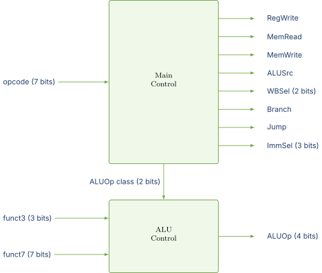
The split into “main control” and “ALU control” is a classical textbook organization due to Patterson [4]. It localizes the opcode-only decisions (everything except the ALU operation within OP-class) in one block and the OP-class refinement in another. The two blocks are both combinational and run in parallel within a single cycle.
Main control as a sum-of-products
For each opcode, list which signals are asserted and which are deasserted. The main control’s truth table has one row per opcode value, so the nine instructions of the running example need only six rows. ADD, SUB, AND, and OR share the opcode 0110011, so their four rows in the table below collapse into a single main-control row and differ only in the ALU operation that the ALU control stage supplies. The other five rows are ADDI, LW, SW, BEQ, and JAL, with the don’t-care entries left undefined.
In SystemVerilog, the main control is a case statement on the opcode that assigns the control signal vector for each case. The synthesizer flattens the case statement into a PLA-like structure. The control signal latency is one to two gate delays.
ALU control as a small lookup
The ALU control’s input is the 2-bit ALUOp class plus funct3 (and, for OP-class only, funct7[5]). The output is the 4-bit ALUOp. The truth table:
Table 3. ALU control mapping. ALUOp class is from main control. funct7[5] distinguishes ADD/SUB and SRL/SRA. Other entries are don’t care.
| ALUOp class | funct3 | funct7[5] | ALUOp |
|---|---|---|---|
| 00 (LW/SW/ADDI) | X | X | ADD |
| 01 (BEQ) | X | X | SUB |
| 10 (OP) | 000 | 0 | ADD |
| 10 (OP) | 000 | 1 | SUB |
| 10 (OP) | 001 | X | SLL |
| 10 (OP) | 010 | X | SLT |
| 10 (OP) | 011 | X | SLTU |
| 10 (OP) | 100 | X | XOR |
| 10 (OP) | 101 | 0 | SRL |
| 10 (OP) | 101 | 1 | SRA |
| 10 (OP) | 110 | X | OR |
| 10 (OP) | 111 | X | AND |
The table is small enough to encode by hand in a few lines of SystemVerilog. The synthesized logic is a handful of gates.
SystemVerilog skeleton
Hardwired main control skeleton for RV32I
module rv32i_main_control (
    input  logic [6:0] opcode,
    output logic       reg_write,
    output logic       mem_read,
    output logic       mem_write,
    output logic       alu_src,
    output logic [1:0] wb_sel,
    output logic       branch,
    output logic       jump,
    output logic [1:0] alu_op_class,
    output logic [2:0] imm_sel
);
    always_comb begin
        // default deassertions
        reg_write    = 1'b0;
        mem_read     = 1'b0;
        mem_write    = 1'b0;
        alu_src      = 1'b0;
        wb_sel       = 2'b00;
        branch       = 1'b0;
        jump         = 1'b0;
        alu_op_class = 2'b00;
        imm_sel      = 3'b000;

        unique case (opcode)
            7'b0110011: begin  // OP (R-type)
                reg_write    = 1'b1;
                alu_op_class = 2'b10;
            end
            7'b0010011: begin  // OP-IMM (I-type)
                reg_write    = 1'b1;
                alu_src      = 1'b1;
                imm_sel      = 3'b000;  // I
            end
            7'b0000011: begin  // LOAD
                reg_write    = 1'b1;
                mem_read     = 1'b1;
                alu_src      = 1'b1;
                wb_sel       = 2'b01;   // MEM
                imm_sel      = 3'b000;  // I
            end
            7'b0100011: begin  // STORE
                mem_write    = 1'b1;
                alu_src      = 1'b1;
                imm_sel      = 3'b001;  // S
            end
            7'b1100011: begin  // BRANCH
                branch       = 1'b1;
                alu_op_class = 2'b01;
                imm_sel      = 3'b010;  // B
            end
            7'b1101111: begin  // JAL
                reg_write    = 1'b1;
                jump         = 1'b1;
                wb_sel       = 2'b10;   // PC+4
                imm_sel      = 3'b011;  // J
            end
            default: ;  // illegal: all deasserted
        endcase
    end
endmodule
The synthesizer converts this into combinational logic in a few dozen lookup-table cells (LUT-4 or LUT-6 in an FPGA). The total area is negligible compared with the register file, ALU, and memory ports.
07.Microcode in Other Modern Processors
x86 is not alone in retaining microcode. Other modern processors use microcode for specific roles.
ARM A64
ARM A64 cores have largely hardwired decoders. ARM’s publicly released technical reference manuals (e.g. [5]) describe instruction execution in terms of architectural semantics without exposing a microcode layer. However, ARM does keep a microcode-like sequencer for certain complex sequences. Load-pair and store-pair instructions on older cores sometimes expand into two micro-ops. The SVC (supervisor call) and HVC (hypervisor call) exception entry sequences traverse small internal sequencers. The bulk of integer and floating-point execution is hardwired.
POWER and other large RISCs
IBM POWER processors use hardwired decode for the vast majority of instructions but retain microcode (or its equivalent) for exception entry, decimal arithmetic, and a few legacy instructions inherited from the original POWER1. The same pattern applies to SPARC and to the older DEC Alpha.
Embedded microcontrollers
Tiny microcontrollers (ARM Cortex-M0, RISC-V PicoRV32) often use multi-cycle execution rather than pipelining, with microcoded or quasi-microcoded sequencers that walk each instruction through fetch, decode, execute, and writeback. The next chapter (Chapter 27) develops this organization in detail.
08.When Microcode Wins, When Hardwired Wins
The choice between microcoded and hardwired control is governed by four factors.
Instruction set complexity
Simple ISAs (RV32I, ARM A64 base) favor hardwired control. The combinational decode logic is small and fast. The microcode ROM would add storage area for no benefit. Complex ISAs (x86, mainframe System/z, legacy CISC) favor microcoded or hybrid control. The ROM amortizes the cost of implementing thousands of rare instruction encodings.
Clock frequency target
At very high clock frequencies (5 GHz and above), microcode adds a cycle of front-end latency that can hurt branch misprediction recovery time. Hardwired decoders integrate more directly into the pipeline’s front-end stages.
Field-update requirement
If the processor needs to support post-fabrication bug fixes, microcode is the only option. Hardwired control cannot be patched. This is one of the strongest reasons modern x86 retains microcode for complex instructions.
Verification burden
Hardwired control with a few hundred gates can be exhaustively verified by formal methods. Microcode with hundreds of routines requires architectural test programs and is harder to verify formally. For safety-critical or certifiable designs (automotive, aerospace, medical), hardwired control is preferred for this reason.
The historical trajectory is clear. The 1950s through 1980s were the era of microcode (System/360, VAX, Motorola 68000). The 1980s RISC movement (MIPS, SPARC, ARM, Alpha) was the era of hardwired control. The 1990s saw the convergence in x86 toward hybrid control with hardwired simple paths and microcoded complex paths. RISC-V in 2010 returned to pure hardwired control with a clean slate. The pendulum may swing back if some future ISA accumulates complexity, but RISC-V is currently the asymptote of simplicity.
09.Worked Examples
10.Exercises
References
- [1]Wilkes, Maurice V. (1951). “The Best Way to Design an Automatic Calculating Machine.” In Report of the Manchester University Computer Inaugural Conference, pp. 16--18.
- [2](2024). “Intel.”
- [3](2024). “AMD64.”
- [4]Patterson, David A. and Hennessy, John L. (2020). “Computer Organization and Design RISC-V Edition: The Hardware Software Interface.” Morgan Kaufmann.
- [5](2024). “ARM.”