The Multi-Cycle Datapath
September 8, 202625 min readintermediate
The single-cycle CPU in Chapter 25 sets its clock period by the slowest instruction’s longest combinational path. The load (LW) traverses the instruction memory, the register file, the ALU, and the data memory…
The single-cycle CPU in Chapter 25 sets its clock period by the slowest instruction’s longest combinational path. The load (LW) traverses the instruction memory, the register file, the ALU, and the data memory in series, taking 9.1 ns in the numerical example. Every other instruction pays the same 9.1 ns clock period even though most finish their combinational work in 7 ns or less. A typical RV32I program spends roughly 30% of its instructions on loads and stores. The other 70% are arithmetic and branches that complete in less time, but in a single-cycle design they wait the full clock period anyway.
The multi-cycle design fixes this inefficiency. Instead of executing each instruction in one long cycle, it breaks the instruction into several shorter phases. Each phase fits in a short clock period (say 2 ns). Arithmetic instructions take four phases (eight nanoseconds total) and branches take three (six nanoseconds). Loads take five phases (ten nanoseconds total). The average is dominated by the common-case arithmetic, not the worst-case load. As a bonus, the same physical ALU, the same memory port, and (often) the same adder can be reused across the phases, saving area.
This chapter develops the multi-cycle RV32I datapath. It starts from the single-cycle picture, identifies the natural phase boundaries, introduces the internal registers that hold intermediate state between phases, builds the finite state machine that sequences the control signals across cycles, and analyzes the CPI trade-off concretely. The chapter closes with the historical context: why the first commercial RISC processors of the early 1980s used multi-cycle designs before the industry transitioned to pipelining in the mid-1980s.
01.Why Multi-Cycle Preceded Pipelining
The multi-cycle design occupies a specific historical niche. From the late 1950s through the early 1980s, computer hardware budgets were dominated by the cost of arithmetic and memory units. A pipelined design, which replicates the datapath into five or more independent stages, was simply too expensive in transistor count for the available technology. A multi-cycle design, which uses one physical ALU and one memory port across all instruction phases, fit the available silicon area.
Transistor budgets, 1970 versus 1990
In 1970, a typical integrated circuit had on the order of 1000 transistors. The Intel 8080 (1974) had 4500 transistors. The MOS 6502 (1975), used in the Apple II and Commodore 64, had 3500. A fully pipelined CPU at this transistor budget was impossible. Multi-cycle execution with shared functional units was the only viable option.
By 1990, transistor budgets had grown three orders of magnitude. The Intel 80486 (1989) had 1.2 million transistors. The MIPS R2000 (1985) had 110,000 transistors and used a 5-stage pipeline. Pipelining became the standard once transistor budgets allowed it.
Multi-cycle as the bridge
Through the first half of the 1980s, multi-cycle was the standard RISC organization. The IBM 801 (1980), the Berkeley RISC I (1981), and the Stanford MIPS (1981) were all multi-cycle. The DEC VAX (1977), although CISC, used heavy microcoding on a multi-cycle engine. The early Motorola 68000 family executed each instruction over 4 to 30 microcycles.
When pipelining became standard in the mid-1980s, the multi-cycle design did not vanish. It moved into embedded microcontrollers, where area and power matter more than peak throughput. The ARM Cortex-M0 (2009) uses a 3-stage pipeline that is closer to a multi-cycle design than to a full RISC pipeline. The PicoRV32 RISC-V core (2015), targeted at FPGAs, is multi-cycle with a configurable CPI.
02.Identifying Instruction Phases
The first step in building a multi-cycle CPU is identifying the natural phase boundaries of instruction execution. From the single-cycle datapath of Chapter 25, the execution of an instruction proceeds through five distinguishable activities.
The five canonical phases
Fetch (IF). Read the instruction word at the address in the program counter. Increment the PC by 4 (or compute the branch/jump target later). This phase exercises the PC and the instruction memory.
Decode and register read (ID). Decode the opcode, read the source registers rs1 and rs2 from the register file, sign-extend any immediate. This phase exercises the decoder, the register file’s read ports, and the immediate generator.
Execute (EX). Perform the ALU operation. For arithmetic this computes rs1 op rs2 or rs1 op immediate. For loads and stores it computes the effective address. For branches it computes rs1 - rs2 (to set the zero flag) and PC + offset. This phase exercises the ALU.
Memory access (MEM). For loads, read the word at the ALU-computed address. For stores, write rs2’s value to that address. Arithmetic instructions do nothing in this phase.
Writeback (WB). Write the result (from the ALU output or from the memory load) back into the register file. Stores and branches do nothing in this phase. The PC was already updated in the fetch phase, so no PC write happens here.
Which instructions use which phases
Table 1. The phases used by each RV32I instruction class. means active, blank means idle (or skipped).
| Instruction | IF | ID | EX | MEM | WB |
|---|---|---|---|---|---|
| ADD/SUB/AND/OR (R-type) | |||||
| ADDI (I-type arith.) | |||||
| LW | |||||
| SW | |||||
| BEQ | |||||
| JAL |
R-type and I-type arithmetic instructions skip the MEM phase because they do not touch data memory. SW skips the WB phase because it does not write a register. BEQ skips both MEM and WB. The multi-cycle controller exploits these skips: if an instruction does not need a particular phase, the controller advances directly to the next one.
03.The Multi-Cycle Datapath Structure
The multi-cycle datapath retains all the functional blocks of the single-cycle version but adds internal registers between them. Each internal register holds the value computed in one phase for use in a later phase.
The internal registers
Instruction Register (IR). Holds the instruction word fetched in the IF phase. Used by the ID phase to extract rs1, rs2, rd, funct3, funct7, and opcode. Persists across all phases of one instruction.
A and B registers. Hold the values read from the register file’s two read ports in the ID phase. Used by the EX phase as ALU operands. The names follow the Patterson-Hennessy textbook convention [1].
ALUOut register. Holds the ALU result computed in the EX phase. Used by the MEM phase (as an address) or by the WB phase (as the value to write back).
Memory Data Register (MDR). Holds the value read from data memory in the MEM phase. Used by the WB phase for loads.
Shared functional units
The multi-cycle design typically merges the instruction memory and data memory into a single memory port. The same physical memory holds both instructions and data, accessed in different phases. The IF phase reads the instruction from address PC. The MEM phase reads (for loads) or writes (for stores) data at the ALU-computed address. A multiplexer on the memory’s address port selects between PC (during IF) and ALUOut (during MEM).
The single ALU is shared across phases. In the IF phase it computes PC + 4. In the ID phase it computes the branch target, PC + imm, and leaves it in ALUOut. In the EX phase it computes the instruction’s actual ALU operation. The two PC-update adders of the single-cycle design collapse into one.
The ID-phase target computation is speculative. The decoder has not yet finished classifying the instruction when the ALU is set to work, so the machine computes PC + imm for every instruction and simply ignores the result unless the opcode turns out to be a branch. That costs nothing, because the ALU would otherwise sit idle for the whole ID cycle while the register file is being read, and it buys the branch a cycle: the compare in S8 can use the ALU for rs1 - rs2 because the target is already waiting in ALUOut. Without it, BEQ would need a fourth cycle, since one ALU cannot both subtract and add in the same cycle.
The complete multi-cycle datapath
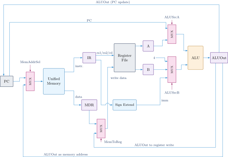
The diagram is denser than the single-cycle version because the internal registers (drawn in violet) sit between every pair of functional blocks. But the functional inventory has actually shrunk. There is one memory port instead of two. There is one ALU and one adder path, not the two adders of the single-cycle version.
04.The Finite State Machine Controller
The control unit for a multi-cycle CPU is no longer purely combinational. It must remember which phase of which instruction it is currently executing. The natural realization is a finite state machine whose states correspond to the instruction phases.
State names
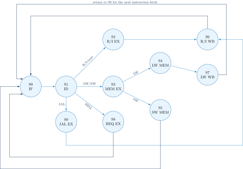
For the nine instruction classes from Chapter 25, the FSM has approximately the following states:
-
S0: Instruction fetch (IF). Always entered first. -
S1: Decode and register read (ID), with the ALU speculatively computing the branch target intoALUOut. Entered from S0. -
S2: Execute for R-type/I-type arithmetic (ALU computation). -
S3: Execute for LW/SW (address calculation). -
S4: Memory access for LW. -
S5: Memory access for SW. -
S6: Writeback from ALU (R-type/I-type/JAL). -
S7: Writeback from MEM (LW). -
S8: Execute for BEQ (compare + branch decision). -
S9: Execute for JAL (jump target + link).
After each state, the FSM transitions either to the next phase of the current instruction or back to S0 to fetch the next instruction. The detailed transitions depend on the opcode read in S1.
Per-state control signal vectors
Each FSM state asserts a specific bit pattern of control signals. The full table is large, but the key entries follow.
Table 2. Selected control signal vectors per FSM state.
| State | PCWrite | IRWrite | MemRead | MemWrite | RegWrite | ALUOp | ALUSrcA | ALUSrcB |
|---|---|---|---|---|---|---|---|---|
| S0 (IF) | 1 | 1 | 1 | 0 | 0 | ADD | PC | 4 |
| S1 (ID) | 0 | 0 | 0 | 0 | 0 | ADD | PC | imm |
| S2 (R-EX) | 0 | 0 | 0 | 0 | 0 | op | A | B |
| S3 (M-EX) | 0 | 0 | 0 | 0 | 0 | ADD | A | imm |
| S4 (LW-M) | 0 | 0 | 1 | 0 | 0 | X | X | X |
| S5 (SW-M) | 0 | 0 | 0 | 1 | 0 | X | X | X |
| S6 (R-WB) | 0 | 0 | 0 | 0 | 1 | X | X | X |
| S7 (LW-WB) | 0 | 0 | 0 | 0 | 1 | X | X | X |
| S8 (BEQ-EX) | cond | 0 | 0 | 0 | 0 | SUB | A | B |
The PCWrite signal in S0 latches PC + 4 into the PC register. In S8 (branch execute), PCWrite is conditional: it is asserted only if the ALU’s zero flag is 1, implementing the branch decision.
Note what S1 and S8 do between them. S1 puts PC + imm into ALUOut, and S8 sets the ALU to SUB for the comparison while writing the PC from the ALUOut value S1 left there. ALUOut is latched at the end of each cycle, so during S8 it still holds the S1 result even though the ALU is busy computing something else. That is what lets one ALU serve a branch in three cycles.
The control unit as code
Multi-cycle FSM skeleton in SystemVerilog
typedef enum logic [3:0] {
    S0_IF, S1_ID, S2_REX, S3_MEX, S4_LWM,
    S5_SWM, S6_RWB, S7_LWB, S8_BEX, S9_JEX
} state_t;

state_t state, next_state;

// State register
always_ff @(posedge clk) begin
    if (reset) state <= S0_IF;
    else       state <= next_state;
end

// Next-state logic
always_comb begin
    next_state = state;
    unique case (state)
        S0_IF: next_state = S1_ID;
        S1_ID: begin
            unique case (opcode)
                7'b0110011: next_state = S2_REX;  // R-type
                7'b0010011: next_state = S2_REX;  // I-type arith
                7'b0000011: next_state = S3_MEX;  // LW
                7'b0100011: next_state = S3_MEX;  // SW
                7'b1100011: next_state = S8_BEX;  // BEQ
                7'b1101111: next_state = S9_JEX;  // JAL
                default:    next_state = S0_IF;
            endcase
        end
        S2_REX: next_state = S6_RWB;
        S3_MEX: next_state = (opcode == 7'b0000011) ? S4_LWM : S5_SWM;
        S4_LWM: next_state = S7_LWB;
        S5_SWM: next_state = S0_IF;
        S6_RWB: next_state = S0_IF;
        S7_LWB: next_state = S0_IF;
        S8_BEX: next_state = S0_IF;
        S9_JEX: next_state = S6_RWB;
    endcase
end

// Output logic: control signals per state
always_comb begin
    // default deassertions ...
    case (state)
        S0_IF: begin
            mem_read = 1'b1;
            ir_write = 1'b1;
            pc_write = 1'b1;
            alu_op   = ALU_ADD;
            alu_src_a = SRC_PC;
            alu_src_b = SRC_FOUR;
        end
        S1_ID: begin
            // No write enables. The ALU computes the branch
            // target speculatively into ALUOut, for every
            // instruction, because the opcode is not classified
            // yet and the ALU is otherwise idle this cycle.
            alu_op    = ALU_ADD;
            alu_src_a = SRC_PC;
            alu_src_b = SRC_IMM;
        end
        // remaining states ...
    endcase
end
The full SystemVerilog module is about 200 lines. The synthesized hardware is on the order of 1000 gates for the FSM state register, the next-state combinational logic, and the output decoder.
05.Functional Unit Sharing
The multi-cycle design’s clearest advantage is that one hardware block serves multiple roles across instruction phases. The same physical ALU performs PC+4 in fetch, address calculation in execute (for loads/stores), and arithmetic operations in execute (for R-type and I-type). Without this sharing the CPU would need three adders. With it, one suffices.
The ALU’s five roles
Table 3. Roles of the single ALU across the multi-cycle phases.
| Phase | Operands | Result |
|---|---|---|
| S0 (IF) | PC, 4 | PC + 4 (next sequential address) |
| S3 (M-EX) | A, immediate | Effective memory address |
| S2 (R-EX) | A, B | Arithmetic result |
| S8 (BEQ-EX) | A, B | Comparison result (zero flag) |
| S9 (JAL-EX) | PC, immediate | Jump target |
The ALU’s two operand inputs require multiplexers. Source A selects among PC and the A register. Source B selects among 4, the B register, and the immediate. Two new control signals (ALUSrcA and ALUSrcB) drive these multiplexers, with the FSM setting them appropriately per state.
The unified memory
A single memory port serves both instruction fetch and data access. The memory’s address input is multiplexed: during S0 (IF) the address comes from the PC, during S4/S5 (LW/SW MEM) the address comes from the ALUOut register. The control signal MemAddrSel drives this multiplexer.
The data port of the memory must also serve dual roles. During IF, the memory’s read output flows into the IR. During LW MEM, it flows into the MDR. During SW MEM, the B register’s value flows into the memory’s write port. The internal-register IRWrite and MDRWrite enables (driven by the FSM) decide which destination latches the memory’s output in any given cycle.
The cost of sharing: structural hazards
The single-cycle design has no structural hazards because each unit is used only once per cycle. The multi-cycle design also has no structural hazards within a single instruction, because each phase uses a different combination of units.
The pipelined design that follows in Chapter 28 introduces the new phenomenon of structural hazards: two different instructions trying to use the same unit in the same cycle. The unified memory of the multi-cycle design becomes a structural hazard in a pipelined design, which is why pipelined designs split it back into separate I-caches and D-caches.
06.Cycles per Instruction Analysis
The multi-cycle design’s headline trade-off is that each instruction now takes multiple cycles. The total execution time of a program in seconds is:
where is the number of instructions executed, is the average cycles per instruction, and is the clock period.
This is the processor performance equation introduced in Chapter 2. Its three factors trade against one another. The single-cycle design has CPI = 1 but a large . The multi-cycle design accepts CPI > 1 in exchange for a smaller .
Per-instruction cycle counts
From the table below, the cycle counts for each instruction class are:
Table 4. Cycle counts per instruction class in the multi-cycle CPU.
| Instruction class | Cycles |
|---|---|
| R-type (ADD, SUB, AND, OR) | 4 (IF, ID, EX, WB) |
| I-type arithmetic (ADDI) | 4 (IF, ID, EX, WB) |
| LW | 5 (IF, ID, EX, MEM, WB) |
| SW | 4 (IF, ID, EX, MEM) |
| BEQ | 3 (IF, ID, EX) |
| JAL | 4 (IF, ID, EX, WB) |
Average CPI for a typical mix
Take a representative integer benchmark mix from Hennessy and Patterson [2]:
-
45% R-type and I-type arithmetic (4 cycles each)
-
20% loads (5 cycles each)
-
10% stores (4 cycles each)
-
15% branches (3 cycles each)
-
5% jumps (4 cycles each)
-
5% other (assume 4 cycles each)
The average CPI is \begin{align*} \overline{\textrm{CPI}} &= 0.45 \cdot 4 + 0.20 \cdot 5 + 0.10 \cdot 4 + 0.15 \cdot 3 + 0.05 \cdot 4 + 0.05 \cdot 4 \\ &= 1.80 + 1.00 + 0.40 + 0.45 + 0.20 + 0.20 \\ &= 4.05 \textrm{ cycles per instruction.} \end{align*}
Comparing total execution time
Suppose the multi-cycle design has a clock period of 2.0 ns (each phase fits in one such cycle). The single-cycle design from a later section has a clock period of 9.1 ns. The ratio of execution times is:
The multi-cycle design takes about 11% less execution time overall for this instruction mix. The advantage is modest because the multi-cycle design pays four to five cycles for instructions the single-cycle design did in one cycle. The win is in the clock period reduction.
Sensitivity to the mix
If the program is load-heavy (40% loads, 30% arithmetic, 15% stores, 10% branches, 5% jumps), the CPI rises to cycles. The advantage narrows. If the program is arithmetic-heavy (60% arithmetic, 10% loads, 10% stores, 15% branches, 5% jumps), the CPI falls to cycles. The advantage widens.
07.Walking Through Two Instructions
A walk-through clarifies how the FSM advances through cycles for two specific instructions.
Tracing ADD x3, x1, x2
Cycle 1 (S0, IF). The FSM is in S0. PC = 0x40. The memory address mux selects PC. The memory reads the instruction at 0x40 (the encoded ADD x3, x1, x2). The ALU computes PC + 4 = 0x44. The IR is loaded with the instruction word. The PC is updated to 0x44. At the next clock edge, the FSM transitions to S1.
Cycle 2 (S1, ID). The decoder reads the IR. It extracts rs1 = 1, rs2 = 2, rd = 3. The register file reads x1 = 7 and x2 = 5 on its two read ports. The A register latches 7, B latches 5. The FSM transitions to S2 (R-EX) because opcode is OP.
Cycle 3 (S2, R-EX). The ALU source A is the A register (value 7). The ALU source B is the B register (value 5). The ALU operation is ADD (decoded from funct3 + funct7). The ALU computes . The ALUOut register latches 12. The FSM transitions to S6 (R-WB).
Cycle 4 (S6, R-WB). The register file write enable is asserted. The write data is the ALUOut register (12). The write address is rd = 3. At the clock edge, register x3 is updated to 12. The FSM transitions back to S0 to fetch the next instruction.
Four cycles, exactly the CPI of an R-type instruction.
Tracing LW x5, 8(x6)
Cycle 1 (S0, IF). As above.
Cycle 2 (S1, ID). The opcode is LOAD. The decoder identifies rs1 = 6, rd = 5, immediate = 8. The register file reads x6. A latches x6’s value. The FSM transitions to S3 (M-EX).
Cycle 3 (S3, M-EX). The ALU source A is A (x6’s value). The ALU source B is the immediate (8). The ALU adds them, producing the effective address. The ALUOut register latches the address. The FSM transitions to S4 (LW-M).
Cycle 4 (S4, LW-M). The memory address mux selects ALUOut. The memory is read. The result loads into the MDR. The FSM transitions to S7 (LW-WB).
Cycle 5 (S7, LW-WB). The register file write port writes MDR into x5. The FSM returns to S0.
Five cycles for the LW.
08.Multi-Cycle vs Single-Cycle vs Pipelined
Place the three organizations side by side.
Table 5. Comparison of the three CPU organizations on nine dimensions.
| Dimension | Single-cycle | Multi-cycle | Pipelined |
|---|---|---|---|
| CPI | 1 | 3–5 | 1.0–1.5 |
| Clock period | Long (worst case) | Short (one phase) | Short (one stage) |
| Functional units | All replicated | Shared | Replicated per stage |
| Pipeline registers | None | Internal regs | Stage regs |
| Control | Combinational | FSM | FSM + hazard logic |
| Memory ports | 2 (I + D) | 1 (unified) | 2 (I + D) |
| Throughput | Lowest | Middle | Highest |
| Area | Middle | Smallest | Largest |
| Verification | Easiest | Moderate | Hardest |
The pipelined design is the de facto industry standard since the late 1980s. It combines the multi-cycle design’s short clock period with throughput close to one instruction per cycle. The cost is the largest area and the most intricate hazard logic. The next chapter (Chapter 28) develops it from the multi-cycle foundation.
09.Worked Examples
10.Exercises
References
- [1]Patterson, David A. and Hennessy, John L. (2020). “Computer Organization and Design RISC-V Edition: The Hardware Software Interface.” Morgan Kaufmann.
- [2]Hennessy, John L. and Patterson, David A. (2019). “Computer Architecture: A Quantitative Approach.” Morgan Kaufmann.