Pipeline Optimization Beyond 5 Stages
September 13, 202619 min readintermediate
The canonical five-stage pipeline of Chapter 29 divides the work of one instruction into five roughly equal slices. At a 1 ns clock period the pipeline executes one instruction per nanosecond in steady state…
The canonical five-stage pipeline of Chapter 29 divides the work of one instruction into five roughly equal slices. At a 1 ns clock period the pipeline executes one instruction per nanosecond in steady state, a peak throughput of 1 GHz times one instruction per cycle. A natural question is whether further subdivision helps. If the five-stage pipeline takes one nanosecond per stage, perhaps a ten-stage pipeline takes 500 ps per stage and runs at 2 GHz. The arithmetic looks clean: cutting the work per stage in half should double the frequency.
In practice, deeper pipelines deliver less than the arithmetic suggests. Every additional stage imposes a fixed latch overhead that is independent of the work done in the stage. Every additional stage between fetch and branch resolution increases the misprediction penalty by one cycle. Every additional stage requires more clock distribution power, more pipeline-register area, and more verification effort. The 1990s and early 2000s saw a steady push toward deeper pipelines, peaking with Intel’s 31-stage NetBurst Pentium 4. The subsequent retreat to 12-to-18 stage designs is one of the most instructive case studies in computer architecture history.
This chapter develops the quantitative model that explains the tradeoff. It derives the optimal pipeline depth in terms of the ratio of latch overhead to per-stage useful work, shows why deeper pipelines amplify the cost of branch mispredictions, and walks through the rise and fall of NetBurst as the canonical illustration.
01.Why Deeper Pipelines Look Attractive
The clock period of a synchronous pipeline is bounded below by the slowest stage, the critical path. If the longest combinational delay between any pair of pipeline registers is , the clock period must satisfy
where is the fixed per-stage cost of the pipeline register itself (Chapter 6). Splitting one stage into two halves the combinational work but does not halve , which is paid once per stage regardless of how much logic the stage contains.
A concrete example clarifies the point. Suppose the original 5-stage RV32I pipeline has ps of useful work per stage and ps of latch overhead, giving ps and GHz. Splitting each stage into two halves produces a 10-stage pipeline with 400 ps of work per stage plus the same 200 ps of latch overhead, for ps and GHz. The clock frequency went up by 67 percent, not 100 percent, because each new stage carries the full latch overhead even though it does only half the work.
The general formula is straightforward. Let be the total combinational work for one instruction (a property of the ISA and the implementation, independent of pipeline depth), and let be the number of pipeline stages. Assuming the work divides evenly across stages:
As grows, shrinks toward zero, and the clock period approaches from above. The clock frequency asymptotes to , a hard ceiling set by the storage technology rather than by the logic. Plot the equation above for ps and ps and the curve rises steeply below , reaches roughly half its 5 GHz ceiling near , and thereafter buys a smaller fraction of the remaining headroom for each stage added.
02.Latch Overhead and Power
The latch overhead has two components. The first is fundamental: setup time, clock-to-Q delay, and margin for skew and jitter. In a modern 7 nm process these total roughly 50 to 80 ps per stage. The second component is the cost of clock distribution: routing the global clock signal to every flip-flop in the pipeline. As the pipeline gets deeper, the clock tree has more terminals and consumes more power.
The dynamic power dissipated by a synchronous circuit (Chapter 9) is approximately
where is the total switched capacitance per cycle and is the activity factor. Doubling the pipeline depth doubles the number of flip-flops, roughly doubles the switched capacitance, and because the architect typically pushes the clock frequency up as well, the power can grow more than linearly with depth. This is the second reason architects do not pursue depth indefinitely: power, not frequency, is the binding constraint in every modern chip.
03.Branch Misprediction Penalty
The most important cost of deeper pipelines is the branch misprediction penalty. When the branch predictor guesses wrong, the pipeline must flush every instruction fetched between the branch and its resolution. The number of flushed instructions equals the number of stages between fetch and the stage where the branch is resolved.
In the 5-stage pipeline of Chapter 29, the branch resolves at the end of the execute stage, which is stage 3 of 5. The misprediction penalty is therefore 2 cycles (the IF and ID stages each held a wrongly-fetched instruction at the moment of resolution). In a 15-stage pipeline that resolves the branch at stage 10, the penalty is 9 cycles. In NetBurst, with a 20-stage pipeline resolving most branches near the back end, the misprediction penalty was about 20 cycles.
The effective CPI of a pipeline with branches is
where is the fraction of instructions that are branches (about 0.15 for typical code), is the branch misprediction rate (5 to 10 percent for a modern predictor, 30 percent or more for a 1-bit predictor), and is the misprediction penalty in cycles. For , , and (the 5-stage pipeline): CPI . Almost ideal. For the same workload on a 20-stage pipeline with the same predictor: CPI . The misprediction tax has grown from 1.5 percent to 15 percent of the ideal runtime.
If the branch predictor improves to (which requires sophisticated multi-table TAGE-style predictors, covered in Chapter 56), the 20-stage CPI drops to , almost recovering the 5-stage figure. This is why deep-pipeline designs ship with expensive branch predictors: the predictor has to keep up with the pipeline depth or the frequency gain evaporates.
04.Optimal Pipeline Depth
Combining the frequency model of the equation above with the CPI model of the equation above yields the instruction throughput (instructions per second):
where is the fraction of pipeline stages between fetch and branch resolution (typically 0.6 to 0.8 for an in-order design). Differentiating with respect to and setting the result to zero gives the optimal depth. After some algebra, the optimum satisfies
The square-root dependence means the optimum is quite sensitive to the predictor quality () and to the latch overhead (). For typical numbers ( ps, , , , ps), the denominator is , so the optimum lands around . This sounds absurdly deep, but the formula ignores power, area, verification cost, and the long tail of other hazards (load-use stalls, cache misses, structural conflicts). Including those costs typically pushes the practical optimum down to to .
Table 1. Pipeline depths for major microarchitectures, in-order and out-of-order. The Cortex-A53 figure is drawn from the public ARM technical reference manual.
| Microarchitecture | Pipeline stages | Notes |
|---|---|---|
| Classic MIPS R2000 (1986) | 5 | The canonical 5-stage |
| MIPS R4000 (1991) | 8 | First “superpipelined” design |
| Intel Pentium (1993) | 5 | Dual-issue, 5 stages |
| Intel Pentium Pro (1995) | 14 | Out-of-order, deeper to absorb misses |
| Intel Pentium 4 (NetBurst) (2000) | 20 | Stretched to 31 stages by 2004 |
| Intel Core 2 (2006) | 14 | Retreat from NetBurst, descended from Pentium M |
| ARM Cortex-A53 (2012) | 8 | In-order, modern smartphone little-core |
| ARM Cortex-A77 (2019) | 13 | Out-of-order, big-core flagship |
| SiFive U74 (2018) | 8 | In-order RISC-V |
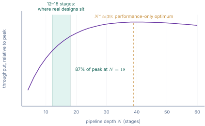
Figure 1 plots that model, and the shape of the curve near its peak matters more than the peak itself.
The depth pattern is clear. In-order designs cluster at 5 to 8 stages. Out-of-order designs (Part V) push depth into the 12 to 18 range because they can hide misprediction penalties through speculative execution. NetBurst is the outlier, and history has not been kind to it.
05.The NetBurst Cautionary Tale
The Intel NetBurst microarchitecture, introduced in the Pentium 4 in November 2000, took deep pipelining to its logical extreme. The initial Willamette core had a 20-stage pipeline. The 2004 Prescott revision stretched it to 31 stages to chase even higher frequencies. At its peak, the Pentium 4 ran at 3.8 GHz on a 90 nm process, a frequency that no out-of-order x86 design would exceed for nearly a decade.
The arithmetic suggested NetBurst should have crushed its competition. A 3.8 GHz Pentium 4 had roughly 1.6 times the clock frequency of the contemporary Athlon 64, which topped out around 2.4 GHz. Yet on most benchmarks the Athlon was faster. Three factors explain the gap.
Misprediction penalty. At 31 stages, a single mispredicted branch flushed on the order of 25 to 30 instructions and cost the equivalent of that many cycles of useful work, well above the roughly 20 cycles the 20-stage Willamette paid. Even with the elaborate trace-cache and branch predictor Intel built for NetBurst, the misprediction penalty was enough to drag effective CPI past 1.5 on branch-heavy code.
Power. The Prescott Pentium 4 dissipated up to 115 W in a desktop part, the highest power figure of any consumer processor of its era. Pushing the clock higher would have required either more voltage (driving power up quadratically per the equation above) or process improvements that did not materialize. Intel’s roadmap had planned a 10 GHz NetBurst by mid-decade. The actual peak was 3.8 GHz.
Memory wall. The pipeline could fetch instructions faster than memory could deliver data. A cache miss to DRAM took hundreds of cycles at the Pentium 4’s clock speed, leaving the deep pipeline stalled waiting for memory. The earlier Pentium III, with its shorter pipeline, paid fewer cycles per memory access in absolute time.
In 2006 Intel abandoned NetBurst and launched the Core microarchitecture, descended from the Pentium M mobile design. Core 2 ran at 14 stages, half NetBurst’s depth, and delivered roughly twice the IPC at lower power. The lesson reverberated through industry: clock frequency in isolation is the wrong metric. The right metric is throughput at a given power budget, and that metric rewards moderate pipeline depths.
06.Modern Sweet Spot: 12 to 18 Stages
Contemporary high-performance cores cluster around 12 to 18 pipeline stages. Intel Golden Cove (covered in Chapter 63) runs about 17 stages. ARM Neoverse N2 (Chapter 62) is about 13. AMD Zen 4 (Chapter 64) sits just above the band at about 19 stages. The convergence is not accidental. Each of these microarchitectures faces similar tradeoffs.
Below 10 stages, the clock frequency is limited by the longest combinational stage, and competitors at higher frequencies win on single-threaded code.
Above 20 stages, the misprediction penalty becomes unmanageable and the latch overhead eats into the frequency gain. Power scales super-linearly because of the larger flip-flop count and the higher clock frequency.
Between 12 and 18 stages, the architect can match the best branch predictors of the era to the depth, keeping CPI close to ideal, while hitting frequencies competitive with the deepest designs without the NetBurst-style power explosion.
A second factor pushes the sweet spot toward this range: out-of-order execution (Part V) can absorb a few cycles of pipeline depth almost for free, because the reorder buffer keeps useful work flowing past a stalled instruction. This is why out-of-order designs (Pentium Pro and after) can run deeper pipelines than in-order designs (Cortex-A53, SiFive U74) without taking the same throughput hit.
07.Variable-Latency Stages and Asymmetric Depth
So far the chapter has assumed all stages take exactly one cycle. Real pipelines have variable-latency operations: integer multiply might take 3 cycles, divide 20, floating-point add 4. These are typically implemented as either (a) a separate functional unit that the main pipeline stalls on, or (b) a deeper sub-pipeline parallel to the main one.
The 5-stage pipeline of Chapter 29 can be extended with an integer multiplier in the execute stage that takes multiple cycles. When a multiply instruction issues, the pipeline holds it in the EX stage until the multiplier produces its result, then advances to MEM. This is structurally simple but causes stalls.
A better approach uses a pipelined functional unit: the multiplier itself is a 3-stage pipeline that accepts one operand pair per cycle and produces one result per cycle with a 3-cycle latency. The main pipeline forwards multiplies to the multiplier’s first stage, then collects the result 3 stages later. Hazard detection becomes more complex (the writeback of a multiply must be delayed past the writeback of a later non-multiply), but throughput improves.
Floating-point pipelines in production designs are typically 3 to 6 stages deep for add and multiply, longer for divide and square root. Chapter 58 (vector microarchitecture) develops these considerations in more detail.
08.Looking Ahead
This chapter closes the concept sequence of Part III with a quantitative model for pipeline depth and the historical case that established the modern 12-to-18 stage sweet spot. A case study, a project, and a lab chapter follow inside Part III and put the model to work. Part IV (Memory Hierarchy) then shifts focus to the second great pipeline-killer: cache misses. A miss to DRAM costs hundreds of cycles, which no in-order pipeline can absorb without help. Out-of-order execution (Part V) is the architectural response, but it depends on the memory hierarchy of Part IV being well-designed enough to keep the cache miss rate low.