Case Study: Open-Source In-Order Cores
September 8, 202624 min readintermediate
The preceding chapters of Part III built the single-cycle datapath (Chapter 25), the control unit (Chapter 26), the multi-cycle datapath (Chapter 27), the introduction to pipelining (Chapter 28), the…
The preceding chapters of Part III built the single-cycle datapath (Chapter 25), the control unit (Chapter 26), the multi-cycle datapath (Chapter 27), the introduction to pipelining (Chapter 28), the five-stage pipeline (Chapter 29), hazard detection and forwarding (Chapter 30), exception handling in the pipeline (Chapter 31), and the deeper-pipeline trade-offs (Chapter 32). Each of those chapters worked from textbook abstractions. This chapter turns to four real cores, all of them open-source or fully documented in public manuals, and traces how the textbook ideas were embodied in working hardware.
Four cores are studied. Berkeley Sodor is the canonical teaching implementation of the five-stage pipeline in Chisel. picorv32 is a deliberately small Verilog core that trades cycles for area. SweRV EH1 is an industrial in-order dual-issue core that powers flash controllers shipping in the millions. ARM’s Cortex-M0+ is a two-stage commercial core whose microarchitecture is documented in a public Technical Reference Manual [1]. Reading the four side by side shows that the same five basic stages and the same hazard-handling mechanisms recur in every implementation, and that the design choices each team made follow from the constraints they were optimizing for.
The chapter uses public sources only. Every claim about a core’s pipeline depth, issue width, area, or instruction set is supported by the core’s public RTL, its README, or its published TRM. No proprietary microarchitecture details from any vendor are introduced.
01.Why Study Real Cores?
A textbook five-stage pipeline is a teaching artifact. It compiles, it simulates, and it executes the RISC-V base ISA correctly, but it sits in a vacuum. It does not have to fit on a particular FPGA, boot a particular operating system, meet a particular timing target, or interface with a particular memory controller. Real cores live in the opposite world. Each one was designed for a deployment, and that deployment shaped every pipeline decision the team made.
Three questions become concrete only by looking at real cores. First, what does the five-stage pipeline studied in Chapter 29 look like when the designer is free to depart from it? Second, where do the textbook stages (fetch, decode, execute, memory, writeback) get split, merged, or overlapped in practice? Third, when a real team faces the area-versus-IPC trade-off introduced in Chapter 28, which way do they go and why?
The answer is not a single best design. Sodor stays close to the textbook because its job is to teach. picorv32 departs from it sharply because area beats IPC for the FPGA market it targets. SweRV EH1 expands the pipeline to nine stages and adds a second issue slot because it must hit gigahertz frequencies on a 28 nm process node. Cortex-M0+ collapses the pipeline to two stages because microcontroller workloads care about interrupt latency more than peak IPC. Four different points in the same design space.
02.Berkeley Sodor
The Sodor family is the closest open implementation to the five-stage pipeline of Chapter 29. Berkeley’s Architecture Research Group developed Sodor as the teaching companion to their graduate computer-architecture course. The source lives at github.com/ucb-bar/riscv-sodor and is written in Chisel 3 plus a small amount of Scala for the testbench infrastructure.
The family ships four cores. The 1-stage core is a pure functional model that completes each instruction in one cycle. The 2-stage core splits fetch from execute. The 3-stage core adds a writeback stage, giving fetch, execute, and writeback. The 5-stage core implements the canonical IF, ID, EX, MEM, WB pipeline with forwarding, stalls, and a static-not-taken branch predictor. All four implement RV32I (the 32-bit base integer ISA). None implement multiply or divide.
Sodor 5-stage pipeline
The 5-stage Sodor core maps almost one-to-one onto the textbook pipeline. Four pipeline registers separate the five stages (dec_reg, exe_reg, mem_reg, and wb_reg in the Chisel source, corresponding to the IF/ID, ID/EX, EX/MEM, and MEM/WB registers of Chapter 29), and a further register named if_reg holds the fetch-stage PC rather than separating two stages. Each of the four is a Chisel Bundle carrying the instruction, the PC, the decoded control signals, and the operand values needed downstream. The hazard detection unit lives in the decode stage and asserts a single stall signal that freezes if_reg and dec_reg and injects a bubble into exe_reg. The forwarding unit, also in decode, selects between the register file output, the EX/MEM forward, and the MEM/WB forward exactly as Chapter 30 described.
The branch handling is static-not-taken. The IF stage predicts that the next PC is PC + 4. When the EX stage resolves a taken branch, it asserts a kill signal that flushes the two instructions already in flight (the one in IF and the one in ID) and redirects the PC. The branch penalty is therefore two cycles on every taken branch and zero cycles on every fall-through, matching the simple branch model of Chapter 30.
Sodor design choices
Sodor optimizes for clarity. Every stage is named, every wire is named, every signal flows through a Chisel Bundle so the data dependencies are visible at the Scala level rather than buried in synthesized Verilog. The control path and the datapath are separated into two Chisel modules, mirroring the textbook separation. The cost of this clarity is that the Verilog Sodor emits is larger than a hand-tuned core would be. The Sodor maintainers state in the README that the target audience is students and instructors, not silicon implementers.
Sodor does not implement the privileged ISA. There is no machine-mode CSR file, no trap handling, and no interrupt controller. The cores boot directly into machine mode with mtvec hardwired to zero, and any exception silently halts the simulation. For a teaching core this is appropriate. For deployment in any real system, those gaps would need to be filled.
03.picorv32
picorv32 is the opposite of Sodor in every design dimension. It was written by Clifford Wolf (now Claire Wolf) in plain Verilog with a single goal: fit as small a RISC-V core as possible into a small FPGA. The source lives at github.com/YosysHQ/picorv32. It implements RV32IMC and is permissively licensed (ISC).
The defining choice in picorv32 is that the pipeline is not a pipeline. picorv32 is a multi-cycle core in the sense of Chapter 27. Each instruction takes between three and forty-plus cycles depending on its type. There is no overlap between consecutive instructions. The ALU, the register file read port, and the memory interface are all shared across phases of a single instruction’s execution.
picorv32 cycle counts
The README documents the cycle count per instruction class. An ALU register-register operation takes three cycles. A branch takes three to five cycles depending on whether it is taken. A load or store takes five cycles plus the memory wait. A multiply takes forty cycles on the unpipelined version and one cycle on the optional pipelined multiplier. Compared to a textbook five-stage pipeline that aims for one cycle per instruction in the steady state, picorv32 is between three and ten times slower per instruction.
picorv32 design choices
picorv32 has no pipeline registers in the textbook sense. The core is a small finite-state machine that walks each instruction through fetch, decode, execute, and writeback in a sequence controlled by a state register. The state machine has between twelve and twenty states depending on the configuration. The result is a design that fits on the smallest commercially relevant FPGAs (the iCE40-LP1K with its 1,280 lookup tables can hold a configured picorv32 with room left for an SoC) while still running real RISC-V code.
The Verilog is written in a deliberately old-school style: no always_ff, no SystemVerilog interfaces, no parameterized modules beyond simple parameter declarations. This is intentional. picorv32 targets the Yosys open-source synthesis flow, and at the time it was written Yosys had patchy support for the newer Verilog features. The constraint reads as a lesson about toolchain coupling: a design’s Verilog dialect is shaped by what its synthesis tool can ingest.
04.SweRV EH1
SweRV EH1 is the production in-order core Western Digital open-sourced in 2019 under the Apache 2.0 license. The source lives at github.com/chipsalliance/Cores-SweRV. SweRV powers the flash translation layer in many of Western Digital’s solid-state drives, so the design choices were made against real-silicon deployment pressure. The published architecture document and the source code are public, but the silicon implementation details are not.
SweRV EH1 implements RV32IMC. The pipeline is nine stages deep, dual-issue (two instructions can issue to two execution units per cycle), and includes a gshare-style branch predictor indexed by a global history register and backed by a return address stack. The core targets 1 GHz operation on a 28 nm process and 600 MHz on a smaller FPGA prototyping board.
Nine pipeline stages
The nine SweRV stages are documented in the SweRV architecture manual. From front to back they are:
-
F1, F2, F3: three stages of instruction fetch, with the branch predictor consulted in F1.
-
Align: a stage that handles 16-bit (compressed) and 32-bit instructions arriving at any byte boundary. This stage was not present in the textbook pipeline because the textbook assumed 4-byte-aligned fetch.
-
Decode: instruction decode and operand read.
-
EX1: first execute stage. ALU operations complete here.
-
EX2, EX3: continuations of execute for longer-latency operations (multiply, divide, load completion).
-
Commit: writeback to the architectural register file.
The depth-to-frequency relationship from Chapter 32 is visible in the design. Each stage carries roughly one fanout-of- four delay budget plus the flip-flop overhead. Three fetch stages absorb the instruction-cache access latency without forcing the clock period to grow.
SweRV design choices
SweRV EH1 demonstrates how an in-order core scales toward production frequencies. The team decided against an out-of-order core because their target workload (flash controller firmware) has predictable instruction patterns and a small enough working set that the branch predictor catches most of the control flow. An out-of-order rename and reorder buffer would have added area and power without proportional IPC gains for the workload.
Three implementation choices stand out. First, the branch predictor is a hybrid of a global-history two-bit-counter table (gshare-like) and a small return address stack, dimensions published in the SweRV manual. Second, the load-store unit supports a single in-flight cache miss plus several already-resolved loads, a simple form of memory-level parallelism. Third, the core keeps interrupt latency in the low tens of cycles while still delivering the throughput of a nine-stage pipeline, which is short enough for the flash-controller firmware it runs. That is not parity with a two-stage microcontroller core, and the worked example at the end of this chapter quantifies the gap.
05.ARM Cortex-M0+
The Cortex-M0+ is ARM’s smallest commercial 32-bit core. It implements the ARMv6-M architecture (the Thumb instruction subset plus a few system instructions) and is documented in a public Technical Reference Manual [1]. The core ships in hundreds of microcontroller families from STMicroelectronics, NXP, Nordic Semiconductor, and Silicon Labs. The TRM is the only public source consulted in this section. The internal RTL is proprietary and is not referenced.
The Cortex-M0+ has a two-stage pipeline. Stage one is fetch. Stage two is decode and execute combined. There is no separate memory stage and no separate writeback stage. Load and store instructions stall the pipeline for one or more cycles while the memory transaction completes. Branches resolve in the execute stage and incur a one-cycle penalty when taken.
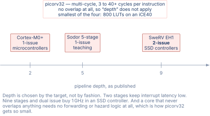
Figure 1 places the four on one axis.
Why two stages?
The two-stage choice is driven by interrupt latency. A microcontroller spends a large fraction of its time servicing interrupts: timers, ADC conversions, UART receives, button presses. The latency from interrupt assertion to the first instruction of the handler running is a first-class metric for this class of core. The ARMv6-M architecture and the Cortex-M0+ microarchitecture together guarantee a 15-cycle worst-case interrupt latency on the standard configuration, including the pipeline flush, the context save (pushing the link register and a few general-purpose registers onto the stack), the vector fetch, and the first handler instruction.
A deeper pipeline would add cycles to the interrupt latency budget because the pipeline flush would discard more in-flight work and the context save would have to drain more pipeline state. Two stages is the shallowest pipeline that still allows the fetch latency to be hidden behind the execute time. One stage (a single-cycle datapath) would have hit a frequency ceiling well below what the microcontroller market demands.
Cortex-M0+ pipeline details
The TRM describes a few additional implementation choices that matter for this case study. The core uses a single-cycle 32-bit multiplier as an optional configuration. The default is a 32-cycle multi-cycle multiplier that costs less area. The instruction set is a 16-bit Thumb subset, so the fetch unit pulls 16-bit half-words from memory. The result is an instruction-side bus interface that moves narrower requests than the 32-bit data side, which keeps the fetch path and its prefetch buffer small.
The Cortex-M0+ does not implement out-of-order execution, branch prediction beyond static-not-taken, instruction caching beyond a small prefetch buffer, or floating point. Each of these omissions is documented as a deliberate trade-off in the TRM. The core is a clean illustration of how aggressively a designer can prune the textbook pipeline when the target market does not need the features being removed.
06.Side-by-Side Comparison
The four cores share an ISA family (Sodor, picorv32, and SweRV are RISC-V, while Cortex-M0+ is ARMv6-M Thumb) and they all execute instructions strictly in program order. They differ in every other parameter that an architect would consider. The table below collects the public numbers in one place.
Table 1. Comparison of four open-source or publicly-documented in-order cores. Numbers are from each core’s README, architecture manual, or Technical Reference Manual. Area numbers vary with process node, target frequency, and configuration, so they are reported as the orders of magnitude each maintainer publishes rather than as a fixed gate count.
| Parameter | Sodor 5-stage | picorv32 | SweRV EH1 | Cortex-M0+ |
|---|---|---|---|---|
| ISA | RV32I | RV32IMC | RV32IMC | ARMv6-M Thumb |
| Pipeline depth | 5 | multi-cycle (3–40+ per instr) | 9 | 2 |
| Issue width | 1 | 1 | 2 | 1 |
| Branch handling | static not-taken | none (in-order finish) | gshare + RAS | static not-taken |
| Forwarding | EX/MEM, MEM/WB | not needed (no overlap) | multiple paths | limited |
| Hazard detection | load-use stall | one instr at a time | full + dual-issue arb. | limited |
| Multiply/divide | not implemented | 40-cycle or pipelined opt. | multi-cycle | optional 1 or 32 cycle |
| Privileged ISA | not implemented | machine-mode only | machine + user | ARMv6-M PMU |
| Target use case | teaching | small FPGA SoC | SSD controllers, 1 GHz | microcontrollers, low latency |
| Area class | large for RV32I (clarity) | smallest (800 LUTs on iCE40) | medium (28 nm production) | smallest commercial 32-bit |
| License | BSD-3 | ISC | Apache 2.0 | ARM IP license |
| Source | UC Berkeley | YosysHQ / Claire Wolf | Western Digital / CHIPS Alliance | ARM TRM |
A few observations follow from the table. The pipeline depth spans from picorv32’s non-pipeline through Cortex-M0+’s two stages, Sodor’s classical five, and SweRV’s production nine. The issue width is one for every core except SweRV, which uses dual issue to lift IPC above unity on workloads with adjacent- instruction parallelism. Branch handling ranges from non-existent (picorv32 has no speculation, so the question is moot) through static not-taken (Sodor and Cortex-M0+) to a full hybrid predictor (SweRV).
07.What the Four Cores Have in Common
Despite the differences in depth and issue width, every core in the table implements the same five logical activities, just split across different numbers of physical stages. Every core fetches an instruction from memory, decodes it, executes it, accesses data memory if needed, and writes the result back. The disagreements are in how to slice those activities. Sodor uses five stages. picorv32 uses one state machine. SweRV uses nine stages and two issue slots. Cortex-M0+ uses two stages.
Every pipelined core in the table also handles hazards through the same three mechanisms introduced in Chapter 30. Stalls freeze the front of the pipeline when a hazard cannot be resolved by forwarding. Forwarding routes values from later stages back to earlier stages so a dependent instruction can proceed. Pipeline flushes (kill signals on Sodor, branch-misprediction flushes on SweRV) discard speculatively-fetched instructions when a branch resolves the wrong way. The names differ across the codebases, but the mechanisms are the same. picorv32 is the one exception, and it is an instructive one. It needs none of the three, because it never overlaps consecutive instructions. Removing the overlap removes the hazards, which is the other way to solve the same problem and the reason its cycle counts are what they are.
Finally, every core treats the program counter as the principal sequencing state. The PC is the input to the fetch logic, the output of the branch resolution logic, and the value saved on trap entry. Every other piece of architectural state (the register file, the CSRs, the memory subsystem) is changed by instructions that the PC selects. This was the architectural contract introduced in Chapter 1 and it carries through unchanged into every real implementation.
08.Reading the Sources Yourself
The chapter so far has summarized public information. The exercises at the end of the chapter ask the reader to confirm the summaries by reading the sources directly. This section gives a short reading guide for each core.
Sodor ships its README, an architecture document under doc/, and the Chisel source under src/main/scala/. Start with the README. Then read rv32_5stage/dpath.scala (the datapath) and rv32_5stage/cpath.scala (the control path) in parallel. The hazard and forwarding logic is concentrated in cpath.scala.
picorv32 ships a single Verilog file (picorv32.v) plus a README and a set of testbench files. The README’s cycle-count table and the state machine in picorv32.v together cover the design. The file is long but readable in one sitting.
SweRV EH1 ships a multi-page architecture manual under docs/, the SystemVerilog source under design/, and a regression test harness. Start with docs/RISC-V_SweRV_EH1_PRM.pdf. The design/dec/ (decode) and design/exu/ (execute) directories are the right entry points to the RTL.
Cortex-M0+ ships a public Technical Reference Manual [1]. Section 1 covers the architectural features. Section 2 covers the pipeline. The TRM is around 100 pages and is readable end-to-end. The RTL is not public, so the case study above relies entirely on the TRM.
09.Worked Examples
10.Exercises
References
- [1](2012). “ARM.”
- [2]Waterman, Andrew and Asanovi\'c (2024). “The RISC-V.”