The Single-Cycle Datapath
September 13, 202629 min readintermediate
Part II spent twelve chapters building the vocabulary of instruction sets. The reader can now read and write RV32I assembly, encode every instruction format by hand, follow a calling convention, and walk…
Part II spent twelve chapters building the vocabulary of instruction sets. The reader can now read and write RV32I assembly, encode every instruction format by hand, follow a calling convention, and walk through an exception handler. What has been missing is the hardware. Part III closes that gap. It builds a working RV32I processor in three architectural styles, single-cycle in this chapter, multi-cycle in Chapter 27, and pipelined starting in Chapter 28.
The single-cycle design is the simplest possible CPU. Every instruction begins on a rising clock edge, propagates through a fixed network of combinational blocks, and finishes by the next rising edge. There are no pipeline stages, no stalls, and no forwarding. The whole machine is one long combinational path clocked once per instruction. The simplicity is pedagogical. No production processor has been built this way since the late 1970s, because the design forces the clock period to track the slowest instruction. But every more sophisticated style, multi-cycle, pipelined, superscalar, out-of-order, builds on the same set of functional blocks introduced here. Understanding the single-cycle datapath end to end is the prerequisite for understanding what pipelining and out-of-order execution actually do.
This chapter constructs the datapath one instruction at a time. It begins with the simplest case (an ADD), then adds the extensions required by ADDI, LW, SW, BEQ, and JAL. Each new instruction adds at most one new functional block and one multiplexer to the diagram. By the end of the chapter the reader has a complete RV32I subset datapath, every wire labeled, every multiplexer’s control signal named. The control unit that asserts those signals is the subject of Chapter 26.
01.What “Execute an Instruction” Means
Before drawing any hardware, fix the operational picture. The processor sits in a steady state with a value in the program counter. Call that value 0x00000040. The instruction memory holds the four bytes starting at that address. On the next clock edge, the processor must:
-
Read the four bytes at address
0x00000040as a 32-bit instruction word. -
Decode the instruction. Identify the opcode, the register operands, and any immediate fields.
-
Read the source registers from the register file.
-
Compute whatever the instruction specifies. For
ADD x3, x1, x2, computex1 + x2. ForLW x5, 16(x6), compute the effective addressx6 + 16, then read that memory location. -
Write the result back somewhere visible. For
ADD, write the sum into the register file atx3. ForLW, write the memory word intox5. ForSW, write the value to memory. -
Update the program counter. For straight-line instructions add 4. For taken branches, add the branch offset. For
JAL, jump to the target.
The single-cycle datapath collapses all six steps into one clock period. Every step happens combinationally during the cycle. The clock edge that ends the cycle latches the result into the register file, into the data memory (for stores), and into the program counter. The clock edge that starts the next cycle uses the new PC value to fetch the next instruction. There is no intermediate state visible to software between cycles.
02.The R-Type Datapath: ADD, SUB, AND, OR
Start with the simplest instructions, the register-register arithmetic ops. The RV32I R-type encoding from Chapter 15 packs three register specifiers (rs1, rs2, rd), a 3-bit funct3, a 7-bit funct7, and a 7-bit opcode into the 32-bit instruction word. The instruction ADD x3, x1, x2 encodes as 0x002081B3, with rs1 = 1, rs2 = 2, rd = 3, and funct3.funct7 = 000.0000000.
The four blocks needed
Four functional blocks suffice for R-type execution. The program counter holds the address of the current instruction. The instruction memory takes that address and produces the 32-bit instruction word. The register file takes rs1 and rs2 as read addresses, produces the corresponding 32-bit values on its two read ports, and accepts a 32-bit value on its write port to be stored at the register named by rd. The ALU takes the two register values and produces a 32-bit result, with the operation (add, subtract, AND, OR) selected by a control signal called ALUOp.
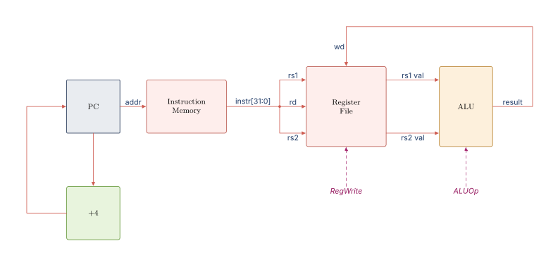
The diagram shows the four blocks and the wires that connect them. Every solid line is a data wire, drawn in coral. Every dashed line is a control signal, drawn in magenta. Two control signals appear: ALUOp chooses the ALU operation, and RegWrite enables writing the result back to the register file. The PC increments by 4 each cycle via a small adder on the lower left.
Walking through ADD x3, x1, x2
Suppose the register file holds x1 = 0x00000007 and x2 = 0x00000005. The PC holds 0x00000040. The instruction memory at 0x00000040 holds the bytes of the instruction 0x002081B3.
-
The PC value
0x40flows into the address input of the instruction memory. The memory’s read port produces the instruction word0x002081B3after its access delay (call it ). -
The instruction word fans out. Bits [19:15] (
rs1= 1) drive the register file’s first read address. Bits [24:20] (rs2= 2) drive the second read address. Bits [11:7] (rd= 3) drive the write address. Bits [14:12] (funct3= 000) and [31:25] (funct7= 0000000) feed the control unit, which decodes them intoALUOp = ADD. -
The register file’s two read ports produce
x1 = 0x00000007andx2 = 0x00000005after its access delay (). -
The two values arrive at the ALU operand inputs. With
ALUOp = ADD, the ALU computes0x00000007 + 0x00000005 = 0x0000000Cafter its delay (). -
The result
0x0000000Csits at the register file’s write data port. WithRegWrite = 1asserted, the next rising clock edge latches it into registerx3. -
Concurrently, the PC adder produces
0x44. The next rising edge latches that into the PC.
By the end of the cycle, the architectural state has advanced by exactly one instruction. The cycle length must accommodate the worst-case sum of the delays above plus setup margin on the register file and PC flip-flops. A later section returns to this calculation.
Extending to SUB, AND, OR
The same datapath handles SUB, AND, and OR without any new wires. Only the ALUOp signal changes. The control unit reads funct3 and funct7 from the instruction word and asserts the appropriate ALUOp encoding. Three bits of ALUOp are enough to distinguish ADD, SUB, AND, OR, XOR, SLL, SRL, and SLT. The ALU itself implements every operation in parallel and a multiplexer at the output selects which result becomes the ALU’s official output. Chapter 11’s project ALU implements the same pattern in Chisel.
03.Adding I-Type Arithmetic: ADDI
The instruction ADDI x5, x6, 12 adds the immediate value 12 to register x6 and writes the result to x5. The encoding is I-type, which packs a 12-bit signed immediate into bits [31:20] of the instruction word.
The R-type datapath cannot execute this instruction. The ALU’s second operand currently comes from the register file’s second read port. For ADDI, the second operand must instead come from the sign-extended immediate. Two changes accommodate this.
The immediate generator
A new block, the immediate generator, takes the instruction word as input and produces a 32-bit sign-extended immediate. For an I-type instruction it copies bits [31:20] to the low 12 bits of its output and replicates bit [31] across the upper 20 bits. The immediate generator handles all five immediate formats (I, S, B, U, J) by routing different instruction bits to different output positions. A 3-bit ImmSel control signal tells the generator which format to use.
The ALU source multiplexer
A 2-to-1 multiplexer placed in front of the ALU’s second operand chooses between the register file’s second read port and the output of the immediate generator. The control signal ALUSrc selects which input wins. For R-type instructions, ALUSrc = 0 and the ALU sees x2’s value. For I-type arithmetic, ALUSrc = 1 and the ALU sees the sign-extended immediate.
Walking through ADDI x5, x6, 12
With x6 = 0x00000010, the instruction ADDI x5, x6, 12 encodes as 0x00C30293 (I-type, immediate = 12, rs1 = 6, rd = 5, funct3 = 000, opcode = OP-IMM).
The instruction memory produces the word. The register file reads x6 = 0x10. The immediate generator extracts the 12-bit field 0x00C, sign-extends it to 0x0000000C, and sends it to one input of the ALU source multiplexer. The control unit sees opcode = 0010011 (OP-IMM) and asserts ALUSrc = 1 and ImmSel = I. The multiplexer passes the immediate. The ALU adds 0x10 + 0x0C = 0x1C, which is latched into x5 at the next rising edge.
04.Adding Loads: LW
The instruction LW x7, 16(x8) reads the 32-bit word at the memory address x8 + 16 and writes it to x7. The encoding is I-type. The 12-bit immediate is 16. The funct3 field (010) identifies the load as a word-sized load. The opcode is LOAD (0000011).
The data memory
A new block, the data memory, has an address input, a write-data input, a read-data output, and two control signals, MemRead and MemWrite. The data memory is conceptually distinct from the instruction memory, although in a real system the two share a single physical memory through caches. The Harvard convention (separate I and D memories at the diagram level) keeps the single-cycle picture clean.
The address calculation
The effective address for a load is rs1 + sign-extended immediate. That is exactly what the ALU already computes when ALUSrc = 1 and ALUOp = ADD. No new arithmetic hardware is needed. The ALU’s existing output wire branches off to the data memory’s address input.
The writeback multiplexer
A second multiplexer (call it the writeback multiplexer) sits in front of the register file’s write data port. It selects between two sources: the ALU output (for R-type and I-type arithmetic) and the data memory’s read output (for loads). The control signal is MemToReg. For arithmetic, MemToReg = 0. For loads, MemToReg = 1.
Walking through LW x7, 16(x8)
Let x8 = 0x00001000 and let the data memory at 0x00001010 hold the word 0xCAFEBABE.
The control unit decodes the LOAD opcode and asserts ALUSrc = 1, ALUOp = ADD, MemRead = 1, MemWrite = 0, MemToReg = 1, and RegWrite = 1.
The register file reads x8 = 0x00001000. The immediate generator produces 0x00000010. The ALU adds them to get 0x00001010. The data memory uses that as its address and produces 0xCAFEBABE on its read port. The writeback multiplexer (with MemToReg = 1) passes the memory value. The next rising edge latches 0xCAFEBABE into x7.
05.Adding Stores: SW
The instruction SW x9, 8(x10) writes the 32-bit value in x9 to the memory address x10 + 8. The encoding is S-type. The 12-bit immediate is split across bits [31:25] and [11:7] of the instruction word, which is why the immediate generator needs an ImmSel input rather than a fixed wire routing.
The store reuses the address-calculation path that the load established. The ALU computes rs1 + immediate. The rs2 value (which is what the instruction wants written to memory) flows from the register file’s second read port directly to the data memory’s write data port. The control unit asserts MemWrite = 1 and RegWrite = 0 (since stores do not produce a register result). The next rising edge writes the memory location.
No new functional blocks are required. The S-type immediate format adds wires inside the immediate generator and a new control signal value for ImmSel, but the rest of the datapath is unchanged.
06.Adding Branches: BEQ
The instruction BEQ x1, x2, offset compares x1 and x2 for equality and, if equal, adds the sign-extended branch offset to the PC instead of incrementing by 4. The encoding is B-type. The 13-bit signed offset is encoded in scrambled order across the instruction word (the least-significant bit is implicit zero because branches target halfword boundaries).
The branch decision
Two pieces of information are needed: whether the comparison succeeds, and what the target address is. For equality the ALU can perform a subtraction and look at whether the result is zero. A single output bit, the ALU’s Zero flag, suffices for BEQ. (For BNE, BLT, and BGE the ALU produces other comparison bits, but Zero alone covers the chapter’s running example.)
The branch adder
A separate adder, drawn beside the PC+4 adder, computes PC + branch_offset. The branch offset comes from the immediate generator (with ImmSel = B). The branch adder exists because the main ALU is already busy computing rs1 - rs2 for the comparison. Two adders are needed because the single-cycle design cannot reuse the ALU for both roles in the same cycle.
The PC source multiplexer
A 2-to-1 multiplexer at the input to the PC chooses between the PC+4 value (for sequential execution) and the PC+offset value (for taken branches). The control signal, call it PCSrc, is the logical AND of the Branch control output and the ALU’s Zero flag. Only when both are 1 does the multiplexer select the branch target.
Walking through BEQ
Suppose x1 = x2 = 0x5, the PC is 0x100, and the branch offset is . The control unit asserts Branch = 1, ALUSrc = 0 (compare with register), ALUOp = SUB, RegWrite = 0, MemRead = 0, MemWrite = 0, and ImmSel = B.
The ALU computes 0x5 - 0x5 = 0, so the Zero flag is 1. The branch adder produces 0x100 + 0x8 = 0x108. The AND of Branch and Zero is 1, so the PC source multiplexer selects 0x108. The next rising edge latches 0x108 into the PC. Execution resumes at the branch target.
If the comparison had failed (x1 not equal to x2), the Zero flag would be 0, the multiplexer would select PC + 4 = 0x104, and execution would continue sequentially.
07.Adding Jumps: JAL
The instruction JAL x1, target writes the return address (PC + 4) into x1 and unconditionally jumps to the J-type immediate offset relative to the PC. The encoding is J-type, with a 21-bit signed offset (low bit implicit zero) packed into bits [31:12] of the instruction word.
JAL requires three small additions. First, the immediate generator needs to handle the J-format encoding (already on its ImmSel list). Second, the writeback multiplexer needs a third input, the value PC + 4, so it can write the return address into the link register. The multiplexer’s control signal expands from one bit (MemToReg) to two bits (typically called WBSel, for writeback select), with encodings for ALU output, memory output, and PC + 4 output.
Third, the PC source multiplexer expands from two inputs (PC+4, PC+branch) to three inputs (PC+4, PC+branch, PC+J-immediate). The control signal expands accordingly. For JAL the multiplexer is forced to the jump target unconditionally, with no dependence on a comparison flag.
Walking through JAL x1, 64
PC = 0x200. The control unit asserts Jump = 1, RegWrite = 1, WBSel = PC+4, and ImmSel = J. The immediate generator produces 0x00000040. The jump-target adder (which can be a small adder beside the branch adder, or the branch adder reused with a different immediate route, depending on the design) produces 0x240. The writeback multiplexer selects the PC+4 path (0x204) and the next rising edge latches it into x1. The PC source multiplexer selects 0x240 and the next rising edge latches it into the PC.
After the cycle, x1 = 0x204 (the return address) and the PC is 0x240 (the call target).
08.The Complete Datapath
The cumulative datapath now handles ADD, SUB, AND, OR, ADDI, LW, SW, BEQ, and JAL. Every instruction class added at most one new functional block (immediate generator, data memory, branch adder) and one new multiplexer. The complete subset datapath has the following components.
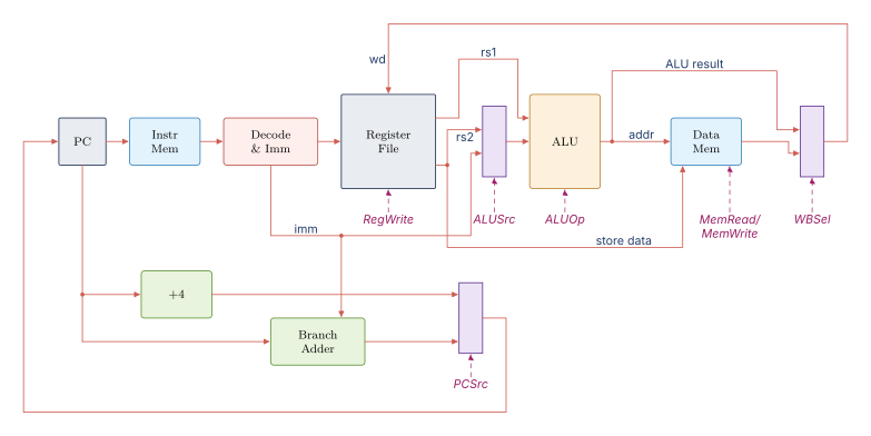
Counting the parts:
-
One PC register (32-bit flip-flop array).
-
One instruction memory (read port only).
-
One register file (two read ports, one write port).
-
One ALU (combinational arithmetic and logic).
-
One data memory (read and write ports).
-
One immediate generator (combinational rewiring of instruction bits).
-
Two adders for the PC-update path (one for PC+4, one for PC+branch offset).
-
Four to five multiplexers (ALU source, writeback select, PC source, plus internal mux inside the immediate generator).
The control signals named so far are RegWrite, MemRead, MemWrite, ALUSrc, ALUOp, WBSel (replacing the original MemToReg), Branch, Jump, PCSrc, and ImmSel. Some of these are derived (PCSrc from Branch AND Zero, for example), and others are direct outputs of the control unit. The next chapter (Chapter 26) derives them systematically from the opcode and function fields.
09.Clock Period and the Worst-Case Path
The single-cycle clock period must be long enough for the slowest instruction’s longest combinational path to settle before the next rising edge. Which instruction is the slowest?
Per-instruction delay sums
Assume the following nominal delays (in arbitrary time units, but proportional to a 1990s 250 nm CMOS process):
Table 1. Nominal delays for the single-cycle building blocks. Times in nanoseconds.
| Block | Delay (ns) |
|---|---|
| PC flip-flop clock-to-Q | 0.5 |
| Instruction memory read | 2.0 |
| Decode and immediate generate | 0.5 |
| Register file read | 1.0 |
| ALU | 2.0 |
| Adder (PC+4, branch target) | 2.0 |
| Data memory read | 2.0 |
| Data memory write setup | 1.0 |
| Multiplexer | 0.3 |
| Register file write setup | 0.5 |
| PC flip-flop setup | 0.5 |
Walk through each instruction class.
R-type (ADD): PC clock-to-Q + IMEM + decode + RF read + mux (ALUSrc) + ALU + mux (WBSel) + RF write setup = ns.
I-type (ADDI): identical to R-type since the immediate generator works in parallel with the register file read. Total ns.
LW: PC clock-to-Q + IMEM + decode + RF read + mux + ALU + DMEM read + mux + RF write setup = ns.
SW: PC clock-to-Q + IMEM + decode + RF read + mux + ALU + DMEM write setup = ns.
BEQ: PC clock-to-Q + IMEM + decode + RF read + mux (ALUSrc) + ALU (compare) + PC mux + PC setup = ns.
JAL: PC clock-to-Q + IMEM + decode + branch adder + PC mux + PC setup = ns.
The worst case sets the clock
The longest path is the load (LW) at 9.1 ns. The minimum clock period for this single-cycle design is therefore 9.1 ns, which translates to a maximum clock frequency of about 110 MHz. Every instruction, even the simpler R-type, must wait the full 9.1 ns because there is no facility to release the next instruction early.
10.Strengths and Weaknesses
The single-cycle design has a few genuine virtues.
Strengths
Conceptual simplicity. Every instruction begins and ends at a rising clock edge. There is no state to track between cycles beyond the architectural state (PC, register file, memory). Debugging amounts to checking the values on the wires at the end of each cycle.
Easy to verify. The combinational portion of the design can be modeled in a single function from inputs (PC, instruction word, register file contents, memory contents) to outputs (new PC, register file write, memory write). Formal verification tools handle such a function readily.
No hazards. Because every instruction completes before the next one begins, there are no read-after-write hazards between instructions, no control hazards from branches, and no structural hazards from shared functional units. The hazard analysis that occupies the next several chapters does not apply.
One control signal set per cycle. The control unit is purely combinational. It reads the current instruction and emits a vector of control signals. There is no microcode sequencer, no pipeline-register-spanning state, no hazard-detection logic.
Weaknesses
Clock period dominated by worst case. As demonstrated above, every instruction pays the clock-period tax of the slowest instruction. For RV32I that slowest instruction is the load, whose path traverses the instruction memory, register file, ALU, and data memory in series. Faster instructions waste the difference.
Hardware reused only once per cycle. The ALU runs for at most one operation per cycle. The data memory is accessed only during loads and stores. The branch adder runs only for branches. A multi-cycle or pipelined design could reuse each unit across multiple instructions, amortizing its area cost.
No parallelism. Only one instruction is in flight at a time. A pipelined CPU executes five or more instructions simultaneously, each in a different stage, multiplying throughput without changing the per-instruction critical path.
Area is not cheap. The single-cycle design needs two adders in the PC-update path (PC+4 and PC+branch). The data memory and instruction memory are physically distinct in the diagram. A multi-cycle design can share a single memory port and a single adder across instruction phases, saving area at the cost of cycle count.
Why study single-cycle anyway
No commercial RV32I processor is built single-cycle. The design is too slow to be competitive with multi-cycle and pipelined alternatives at the same area budget. But the single-cycle datapath is the foundation on which every more sophisticated design is built. The pipeline registers introduced in Chapter 28 slice exactly this datapath into five stages. The forwarding paths added in later chapters route around exactly these multiplexers. The gem5 out-of-order CPU model used in Chapter 66 begins from this picture and adds structure.
The reader who can draw the complete single-cycle RV32I datapath from memory, label every wire and control signal, and trace any instruction through it in a single cycle has the foundation needed for everything that follows in Parts III through V.
11.What Is Missing from This Picture
The chapter has built enough datapath to execute eight or nine RV32I instructions. The full RV32I has 47 base instructions. The gaps that remain:
Other arithmetic. XORI, ORI, ANDI, SLLI, SRLI, SRAI, SLT, SLTU, SLTI, SLTIU, and XOR, SLL, SRL, SRA, SLTU extend the ALU’s operation list. None require new datapath structure, only a wider ALUOp encoding.
Other memory ops. LH, LB, LBU, LHU, SH, and SB need a small block in front of the writeback multiplexer that sign-extends or zero-extends the loaded byte or halfword to 32 bits. The data memory itself needs byte-enable signals on the write port.
Other branches. BNE, BLT, BGE, BLTU, and BGEU compare the ALU output against different conditions. The ALU produces a small bundle of comparison flags (zero, negative, carry-out, overflow) and a comparator block picks the right one based on funct3.
Other jumps. JALR (jump and link register) adds the immediate to a register rather than to the PC. The jump-target adder needs a 2-to-1 multiplexer in front of one of its inputs to select between the PC and the register value.
Upper-immediate instructions. LUI and AUIPC load a 20-bit immediate into the upper bits of a register. They reuse the immediate generator (with the U format), the ALU (for AUIPC, which adds the immediate to the PC), and the register file write port.
System instructions. ECALL, EBREAK, and the CSR instructions require the privilege machinery covered in Chapter 20. The basic datapath does not change much, but the control unit extends and a CSR file is added.
Adding these instructions follows the same recipe used throughout the chapter. Identify what new functional unit is needed (often none), identify what new multiplexer is needed, and name the new control signal. The complete RV32I datapath has perhaps ten or twelve multiplexers and twelve to fifteen control signals, but the structure remains the same.