Power, Frequency, and Thermal
September 13, 202627 min readadvanced
The earlier parts of this book treated performance as the primary objective. Chapter 2 introduced Moore’s law, Dennard scaling, and the processor performance equation. The intervening parts on ISAs (Part II)…
The earlier parts of this book treated performance as the primary objective. Chapter 2 introduced Moore’s law, Dennard scaling, and the processor performance equation. The intervening parts on ISAs (Part II), pipelining (Part III), the memory hierarchy (Part IV), and the out-of-order machinery of the preceding chapters of Part V all sized structures with the goal of raising instructions per cycle and clock frequency. The implicit assumption was that power followed performance, that faster always meant better, and that the architect’s job was to extract more performance from any silicon budget.
That assumption ended in the mid-2000s. Chapter 2 documented the end of Dennard scaling around 2005. The flat-line in single-thread frequency from that point onward is the most visible consequence. The deeper consequence is that every modern processor now spends as much engineering effort on power management as it does on raw performance. The voltage regulator, the on-chip clock controllers, the thermal sensors, the per-domain power gates, the workload classifiers, and the firmware that runs DVFS are not afterthoughts. They are co-equal with the rename stage and the issue queue in the design of a 2026-era out-of-order core.
This chapter revisits the power equation at the scale of a modern OoO core. It walks the voltage-frequency curve, derives why dynamic voltage and frequency scaling pays for itself, examines race-to-idle as the policy that emerges when static power dominates, surveys dark silicon as the unavoidable consequence of the failure of Dennard scaling, and traces thermal throttling and turbo boost as the two faces of the same opportunistic power-budget allocation. The chapter closes with the AVX-512 frequency cliff as a concrete case study of how vector width interacts with the power-management subsystem on Intel server cores.
01.The Power Equation Revisited
The dynamic power dissipated by a CMOS gate that switches its output is
where is the activity factor (the fraction of cycles in which the gate switches), is the load capacitance the gate drives, is the supply voltage, and is the clock frequency. The total dynamic power of the chip is the sum of this term across every switching gate, plus a contribution from clock-tree distribution.
The static (or leakage) power is
where depends exponentially on temperature , on the supply voltage , and on the threshold voltage of the transistors. Leakage rises rapidly with temperature, which is one reason a hot chip is also a less efficient chip.
Three observations follow directly from the equation above and shape every design choice in this chapter.
First, the dynamic-power term is quadratic in voltage and linear in frequency. Halving voltage reduces dynamic power by a factor of four. Halving frequency reduces dynamic power by only a factor of two. This asymmetry is the foundation of DVFS: dropping voltage is much more valuable than dropping frequency.
Second, the maximum sustainable frequency at a given voltage follows the alpha-power law, roughly , where the exponent is close to for long-channel devices and falls to roughly at the velocity-saturated short-channel transistors of modern nodes. Reducing voltage forces a reduction in frequency, and because the exponent sits below two, the frequency bought by each additional increment of voltage shrinks as the supply rises. Read the other way around, the voltage a target frequency demands climbs faster and faster as that target rises, which is the convexity captured in the voltage-frequency curve plotted in Figure 1.
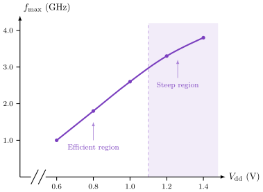
Third, static power does not depend on activity factor. A chip that sits idle at with set to zero still leaks. To reduce leakage when a block is idle, the architect must power-gate the block, cutting its to zero rather than just its clock.
Worked example: superlinear scaling at the high end
A core operates at with a measured dynamic power of W. The architect proposes to raise the operating point to . Estimate the new dynamic power, assuming the activity factor and switched capacitance are unchanged.
The ratio is So the new dynamic power is roughly W. The 50% frequency increase comes at a 134% power increase. Dynamic power grows as the full cube of frequency only when the supply voltage rises in proportion to the frequency. Here the voltage rises by 25% while the frequency rises by 50%, so the effective exponent is about rather than . Even at that exponent the high end of the voltage-frequency curve is brutal for energy efficiency, and this is the regime where turbo boost operates.
02.Dynamic Voltage and Frequency Scaling
DVFS is the runtime mechanism that exploits the curvature of the voltage-frequency relationship. A processor exposes a discrete set of operating points, each a (voltage, frequency) pair pre-validated by silicon characterization. A controller selects among the points to match instantaneous workload demand to instantaneous power and thermal headroom.
Operating points (P-states)
The Advanced Configuration and Power Interface (ACPI) standard names the operating points P-states. P0 is the highest-performance state (maximum voltage and frequency). P1, P2, , are progressively lower-performance, lower-power states. A modern x86-64 core typically exposes 10 to 20 P-states. ARM cores follow the same pattern through their own operating-point tables.
Table 1. Typical P-state table for a desktop core
| P-state | Frequency (GHz) | Voltage (V) | Estimated dynamic power (W) |
|---|---|---|---|
| P0 | 4.5 | 1.20 | 95 |
| P1 | 4.0 | 1.10 | 71 |
| P2 | 3.5 | 1.00 | 51 |
| P4 | 3.0 | 0.95 | 39 |
| P6 | 2.5 | 0.90 | 30 |
| P8 | 2.0 | 0.85 | 22 |
| P10 | 1.5 | 0.80 | 14 |
| P12 | 1.0 | 0.75 | 9 |
Illustrative table only. Actual P-state ranges are microarchitecture-specific. Source: representative values from the Intel SDM [1] and the AMD APM [2].
Who decides the P-state
The controller that decides which P-state is active varies by generation. On older platforms, the operating system’s CPU frequency governor selected the P-state through MSR writes. On modern Intel platforms since Skylake, the hardware power-management unit (HWP) inside the package controls the P-state autonomously, with the OS supplying only a high-level performance hint (EPP, the energy-performance preference). On AMD platforms, P-state Tables are exposed and the OS-side governor still plays a role, with hardware over-ride paths through the System Management Unit (SMU). ARM platforms use the OS’s CPUFreq subsystem with platform-specific drivers.
The HWP / SMU paths are faster than OS-driven DVFS because the hardware reacts on a microsecond time scale rather than a millisecond one. A short burst of work that finishes in a millisecond can be served at P0 and then dropped back to a deep idle state before the OS-driven path would have noticed.
Switching cost
A P-state transition is not free. It takes 10 to 100 microseconds to ramp the voltage regulator’s output and to re-lock the phase-locked loop (PLL) at the new frequency. During the transition, the core typically continues to execute at the old, lower frequency or pauses briefly. The controller has to amortize the transition cost across the workload phase that warranted the change. A controller that switches P-states every microsecond would spend most of its time in transitions and would degrade performance.
The cost has two practical implications. First, P-state transitions have to be infrequent relative to workload phases. A typical production system holds a P-state for milliseconds. Second, fine voltage stepping (separate voltage rails per core) lets one core change voltage without disturbing the others. Modern parts use per-core voltage domains for exactly this reason. Apple’s M-series cores, Intel’s Sapphire Rapids, and AMD’s Zen 4 all expose per-core voltage and frequency control.
03.Race-to-Idle
A counterintuitive result of the equation above is that running faster can save energy. The principle is called race-to-idle: finish the task at the highest available frequency, then drop into the deepest idle state available.
The argument
Energy consumed for a fixed task is
If is small (deep sleep state, leakage minimized through power gating), then completing the task quickly so that stretches over the remaining wall-clock period can produce lower than running slower at a lower for longer. The crossover depends on the ratio between active and idle power.
When race-to-idle wins and when it loses
Race-to-idle wins when the active workload has a low average utilization. A core that is busy for 10% of the time and idle for 90% benefits from completing each burst quickly and idling deeply. The deeper the idle state, the larger the savings.
Race-to-idle loses when the workload is sustained or near-saturated. A core that is busy 90% of the time and idle 10% sees almost all its energy spent in the active state, where the cubic frequency scaling on the voltage-frequency curve dominates. Running at a lower frequency saves more than racing-to-idle does.
A second consideration is the cost of entering and exiting deep idle states. A C-state transition can take tens to hundreds of microseconds, and during the transition the core is neither doing useful work nor saving the full idle-state power. If the average idle interval is shorter than this transition latency, the controller does not enter the deep state, and race-to-idle loses its argument.
Modern firmware blends the two strategies. The HWP / SMU controller estimates workload utilization on a microsecond time scale and biases toward race-to-idle for short bursty workloads, toward sustained mid-frequency operation for steady workloads, and toward deep low-frequency operation for background and unimportant work. The energy-performance preference hint (EPP) lets software bias the controller’s decisions for the active process class.
04.Dark Silicon
The end of Dennard scaling is the deepest reason power-management became a first-class concern. Dennard’s 1974 paper showed that as transistor dimensions shrink by a factor , the supply voltage also shrinks by , so per-transistor power drops as . Doubling the transistor count per unit area at the next node therefore leaves total power per unit area roughly unchanged. From the 1970s through the early 2000s this held to good approximation. Each new node delivered more transistors at the same power.
Why Dennard scaling ended
Two physical phenomena ended Dennard scaling around the 65 nm node. First, subthreshold leakage grew exponentially as had to be lowered to keep up with . By the 90 nm node, leakage was a substantial fraction of total chip power. Second, gate-oxide tunneling currents added a second leakage mechanism. The transistors could no longer be turned fully off without sacrificing speed.
The combined result is that the supply voltage cannot continue to scale down with transistor dimensions. has been roughly flat between 1.0 V and 1.2 V for the past fifteen years. Each new node doubles transistor density, but per-transistor power no longer falls by the full factor. Total chip power budget grows with each generation if every transistor is to be active.
The dark silicon argument
Power is bounded by package thermal design power (TDP), which is roughly fixed by the cooling solution and the form factor. If per-transistor power does not fall fast enough, then each new generation produces a chip with more transistors than can be active simultaneously within the TDP. The fraction that must be unpowered at any one time is the dark silicon fraction.
The architectural responses to dark silicon are several. First, heterogeneous integration: include large blocks of fixed-function accelerators that are turned off most of the time. Each accelerator sits dark when it is not needed and consumes near-zero power. Second, aggressive power gating: every core, every cache slice, and every accelerator block has dedicated power gates that fully shut off its supply when idle. Third, dynamic voltage and frequency scaling on the active blocks to keep the active fraction within the TDP envelope. Fourth, turbo boost, which redirects the TDP budget from idle blocks to active blocks for short windows.
The shift to many smaller specialized blocks rather than a few large general-purpose cores is a direct consequence. The big.LITTLE architectures from ARM (see Chapter 16), the P-core / E-core split on Intel client parts since Alder Lake, and the GPU-plus-NPU-plus-CPU heterogeneity on Apple’s M-series chips are all responses to the dark-silicon constraint.
05.Thermal Throttling
The thermal subsystem is the safety net that prevents the chip from destroying itself. Every modern processor carries on-die temperature sensors that report die temperature to the power-management unit on a microsecond time scale. When the temperature exceeds a threshold (Tjmax, the maximum junction temperature, typically on x86-64 parts and - on ARM parts), the hardware automatically reduces frequency, voltage, or both, until the temperature falls back into the safe range.
Sensor placement and accuracy
The on-die temperature sensors are placed near the hottest expected hotspots. On a multi-core chip there is typically one sensor per core, plus several sensors near the L3 cache, the memory controller, and the I/O blocks. The PMU polls all sensors at a high rate (kHz range) and uses the highest reading to drive the throttle decision. The cores are not independent: one core hitting Tjmax forces package-wide throttling, since the heat from that core spreads to its neighbors.
The accuracy of the sensors is finite. The reported temperature can lag the actual transient temperature by a few microseconds, which is short compared to thermal time constants of milliseconds but long enough that the PMU must include margin in its throttle threshold. Setting the throttle threshold too high risks transient overshoot. Setting it too low gives up performance.
Throttle response
The two levers the PMU has are voltage and frequency. The standard response is to step down the active P-state to a less aggressive operating point. If the temperature continues to climb, the PMU steps further down. In emergency conditions (sensor failure, runaway thermal event), the PMU asserts a hardware signal called PROCHOT (Intel terminology) or its equivalent on other vendors, which forces the core to clock-gate large fractions of the pipeline and idle aggressively. PROCHOT is a defensive measure, not a performance feature.
Skin temperature and laptops
Laptops and mobile devices add a second thermal constraint: the surface temperature where the user touches the device must stay below a comfort threshold (typically for skin contact). The chip can be well within Tjmax and still be forced to throttle because the laptop chassis is too hot.
Apple’s M-series cores, which run in fanless or low-fan-power configurations in the MacBook Air, are particularly sensitive to the skin-temperature constraint. The cores often throttle before they reach Tjmax. Pro variants with active cooling can sustain higher sustained performance at the same Tjmax simply because the fan keeps the surface within comfort range.
06.Turbo Boost
Turbo boost is the mirror image of thermal throttling. When the chip has thermal and power headroom, the PMU opportunistically raises the frequency of active cores above the nominal base frequency. The headroom typically appears when some cores are idle or when a sustained workload has not yet heated the package.
Turbo bins
Turbo states are organized as turbo bins, each one a small frequency step (100 MHz to 200 MHz on modern parts) above the base frequency. The PMU selects the highest bin that satisfies all of (a) the temperature is below Tjmax minus a margin, (b) the package power is below the package thermal design power minus a margin, (c) the current is below the maximum sustainable current the voltage regulator can deliver, and (d) the number of active cores is at or below the per-bin active-core count limit.
The active-core count limit is the source of the per-bin specification on most Intel parts. A part rated "5.5 GHz boost on 1 core, 5.2 GHz on 2 cores, 4.9 GHz on 4 cores, 4.6 GHz on all cores" exposes the constraint plainly. Boosting more cores requires more total power, which forces a lower per-core frequency to stay within the TDP budget.
Table 2. Representative turbo bins on a desktop CPU
| Active cores | Max frequency (GHz) | Estimated package power (W) |
|---|---|---|
| 1 | 5.5 | 60 |
| 2 | 5.2 | 90 |
| 4 | 4.9 | 130 |
| 8 | 4.6 | 170 |
| 16 | 4.3 | 200 |
Illustrative table. Actual turbo bins are documented per SKU in vendor spec sheets [1][2].
Time-windowed power budgets
Intel’s PL1, PL2, PL3, PL4 power-limit hierarchy exposes the time-windowed budget mechanism. PL1 is the sustained power limit, typically equal to TDP, applied over a long time window (28 seconds is a common default). PL2 is the short-term burst limit, higher than PL1, applied over a shorter window (10 to 100 milliseconds). PL3 and PL4 cover instantaneous current limits.
The mechanism lets the part exceed its nominal TDP for short bursts. A user clicking a button that triggers a one-second compute burst can see the chip boost to PL2 power for that burst, exceeding the sustained PL1 limit. The chip averages PL1 over the long window, so sustained workloads see only the nominal power. The PMU integrates the energy delivered, and when the long-window integral catches up to the average TDP budget, it forces the chip back to the lower power level.
AMD exposes the equivalent through Package Power Tracking (PPT), Thermal Design Current (TDC), and Electrical Design Current (EDC) limits.
Predicting turbo behavior
Turbo behavior on real workloads is not deterministic. The starting temperature of the chip, the surrounding ambient temperature, the fan curve, the workload’s instantaneous current draw, and the distribution of activity across cores all affect which bin the PMU selects. Benchmark numbers reported as "boost frequency" reflect the maximum the part can hit under ideal conditions. Sustained turbo behavior on a saturated chip rarely exceeds the all-cores boost bin.
07.AVX-512 Frequency Cliffs
A widely-documented case where vector width interacts directly with the power-management subsystem is Intel’s AVX-512 implementation on Skylake-SP and successor server cores. The 512-bit vector data paths draw substantially more current per cycle than scalar code, because they switch eight times as many lanes per instruction. The voltage regulator and the maximum sustained current limit cannot support full base frequency when AVX-512 is in use.
The cliff
When the core detects AVX-512 issue activity, the PMU drops the operating point to a lower P-state called AVX-512 license level 2 (in contrast to license level 0 for scalar code and license level 1 for AVX2). The frequency drop is microarchitecture- and SKU-specific, ranging from 200 MHz to 600 MHz below the nominal turbo, with a corresponding voltage reduction.
The cliff is automatic. The PMU monitors the AVX-512 active state through a hardware counter that increments when a 512-bit vector operation issues. After a threshold of consecutive issues, the PMU steps down. After a hysteresis period of scalar-only activity, it steps back up.
Why the cliff exists
The cliff exists because the chip’s voltage regulator cannot deliver the current required by AVX-512 at the nominal high-frequency operating point without exceeding the safe transient current limit (EDC on AMD, ICCMAX on Intel). The PMU has two choices when a wide-vector instruction issues: reduce frequency, or risk exceeding the current limit and triggering an emergency throttle (PROCHOT). The pre-validated lower P-state is the controlled response.
Mitigations and workarounds
Several mitigations exist. The compiler can be told to avoid AVX-512 entirely in code paths that mix with non-AVX-512 work. Intel’s later parts (Ice Lake server, Sapphire Rapids) have narrowed the cliff substantially by improving the voltage regulator and reducing the steady-state penalty. The penalty is no longer the 600 MHz that Skylake-SP imposed. Ice Lake server reports a penalty of around 100-200 MHz.
The Arm Scalable Vector Extension (SVE) and SVE2 take a different approach: the vector length is implementation-defined and can be narrower on cores that cannot sustain the full vector width without throttling. The chip never advertises a vector width it cannot sustain. This avoids the cliff at the cost of variable performance across implementations of the same ISA.
08.Power-Aware Microarchitectural Choices
The power equation interacts with most architectural choices made in Part V. Several patterns recur.
Clock gating
The cheapest power optimization is to stop the clock to any pipeline stage that is not doing useful work in a given cycle. A bubble cycle in the execute stage does not need the ALU clock to toggle. The result is a dynamic power saving proportional to the bubble fraction. Every modern OoO design clock-gates at the granularity of individual issue ports, register-file banks, and ROB entries. The infrastructure is invisible to software but contributes substantially to the active power.
Power gating
The cousin to clock gating is power gating: cutting to a block that is not in use. Power gating eliminates both dynamic and static power for that block, at the cost of taking the block offline. The entry and exit latency is typically a few microseconds, so power gating is reserved for blocks expected to be idle for at least that long. Idle cores, idle accelerator blocks, and idle cache slices on the last-level cache are common power-gating candidates.
Width and depth tradeoffs
Wider pipelines (more issue ports, more rename slots, more execute units) extract more ILP but also draw more current per cycle. Deeper pipelines reach higher frequencies but pay a quadratic penalty in dynamic power because the per-stage capacitance is amortized over more cycles per instruction. The optimal point is workload-dependent and is one reason heterogeneous cores (P-cores and E-cores on Intel client parts, big.LITTLE on ARM) have displaced uniform-core designs in client SoCs.
Specialization
The fastest growing power-saving technique is to add a fixed-function accelerator for a common operation. A dedicated video codec engine, a dedicated AES instruction unit, or a dedicated neural-network engine performs the operation at one tenth to one hundredth of the energy per operation of the general-purpose core. The accelerator sits dark when not in use and consumes negligible power. Apple’s Secure Enclave, Apple’s NPU, and the cryptographic acceleration instructions in AArch64 are examples. A full treatment of domain-specific accelerators lies beyond this book.
09.Worked Examples
10.Exercises
References
- [1](2024). “Intel.”
- [2](2024). “AMD64.”
- [3]Esmaeilzadeh, Hadi and Blem, Emily and St. Amant, Renee and Sankaralingam, Karthikeyan and Burger, Doug (2011). “Dark Silicon and the End of Multicore Scaling.” In Proceedings of the 38th Annual International Symposium on Computer Architecture (ISCA), pp. 365--376. doi:10.1145/2000064.2000108