Design for Test and Silicon Debug
September 8, 202645 min readadvanced
You spend two years designing a CPU core. Verification Methodology throws ten billion cycles of constrained-random simulation at it, formal proves the tricky protocol properties, emulation boots an operating…
01.Part 1, the problem manufacturing creates
1.1 A correct design and a broken chip
You spend two years designing a CPU core. Verification Methodology throws ten billion cycles of constrained-random simulation at it, formal proves the tricky protocol properties, emulation boots an operating system. Every known bug is fixed. The design is correct.
Now a fab makes a hundred million copies. One has a speck of dust that landed during lithography and left a 40 nanometre blob of metal bridging two wires in the load queue. Another has a via that did not etch through. A third is electrically perfect but one transistor came out narrow, so a path that should settle in 300 picoseconds takes 340, and the chip works at 2 GHz and produces garbage at 3 GHz.
None of those is a design bug. Verification cannot find them, because verification runs against a model and the model does not have dust in it. Verification proves a property of the design. Manufacturing test proves a property of one specific physical die. Those are claims about different objects.
1.2 Why this is economics, not curiosity
Defects land roughly at random, so the probability a given die area is defect-free is Poisson,
with yield, die area, defect density. Take and per . Then and . Sixteen and a half dies in every hundred are defective, and each must be caught early, because the cost of finding a bad part multiplies by roughly ten at each step downstream. Cents at wafer sort, dollars after packaging, tens of dollars after board assembly, a return and a reputation in a customer's hands.
Now the number that sets the target. If your test catches a fraction of possible faults, the fraction of shipped parts that are secretly bad is the defect level,
quoted in defective parts per million, DPM.
| Coverage | DPM | Field failures per 200 M units | |
|---|---|---|---|
| 0.80 | 0.0354 | 35,400 | 7,080,000 |
| 0.90 | 0.0179 | 17,900 | 3,580,000 |
| 0.99 | 0.0018 | 1,800 | 360,000 |
| 0.999 | 0.00018 | 180 | 36,000 |
Read the last two rows against each other. Moving from 99 percent to 99.9 percent coverage, which sounds like a rounding error, removes 324,000 field failures. That is why engineers argue about the third decimal place of a coverage number.
1.3 Why functional test cannot do this
Reachability. To learn whether one AND gate inside the branch predictor's tag comparator is stuck at 0, you need an instruction sequence steering the machine into a state where both its inputs are 1. There are millions of such gates and nobody generates those sequences automatically for a real core.
Observability. Even when a fault changes an internal value, the difference must survive many more layers of logic to reach a pin. A wrong value entering a mux whose select points elsewhere simply vanishes.
Tester economics. Automatic test equipment costs 3 to 10 cents per second, so a 30 dollar part affords one or two seconds. Booting an operating system takes seconds to minutes and reaches perhaps 80 percent stuck-at coverage, which the table prices at 35,400 DPM. Unshippable, and a thousand times too slow.
So the industry does the only thing that works. Add hardware whose sole purpose is making the chip cheap and thorough to test. That is design for test, and it changes the flop you use, the reset tree, the clock tree, the floorplan, and the power budget.
02.Part 2, fault models
2.1 The abstraction problem
There is no finite list of "all the ways a blob of metal can land," so testing works with fault models, abstractions that must be small enough to enumerate and close enough to reality that patterns detecting every modeled fault also catch defects the model never described. Nothing guarantees the second property. It is an empirical claim, validated by decades of correlation between coverage and field returns.
2.2 Stuck-at, and why something this crude works
The stuck-at model says one net is permanently tied to 0 or 1. Each net gets two faults, so a circuit with nets has exactly faults. Linear, therefore enumerable. A 5 million gate block has roughly 6 million nets and 12 million faults.
Work one by hand. Take and target " stuck-at-0." The good circuit must have , or the fault changes nothing. And must reach , which for an AND gate needs . So the pattern is , giving good and faulty .
| good | -sa0 | -sa1 | -sa0 | -sa0 | |
|---|---|---|---|---|---|
| 0 | 0 | 0 | 0 | 0 | |
| 0 | 0 | 1 | 0 | 0 | |
| 0 | 0 | 0 | 0 | 0 | |
| 1 | 0 | 1 | 0 | 0 |
The last row detects three faults with one pattern, which is the seed of compaction in 4.2 and the reason 12 million faults do not need 12 million patterns.
Why does a model this crude work? Partly because many defects behave stuck-at from outside. A short to ground is stuck-at-0, an unopened via leaves a node that settles to a constant, a transistor failed open in a pull-down network cannot drive low for some inputs. The deeper reason is that detecting all stuck-at faults requires driving every net to both values and making each observable, so the pattern set exercises essentially the whole circuit in both directions and catches defects it was never aimed at. Stuck-at coverage is a proxy for thoroughness of exercise, not a defect inventory. Its limit is equally clear. It is static, with no notion of time, so it cannot describe anything that merely works slowly.
2.3 Transition faults and at-speed test
A transition fault says a net still reaches both values but takes too long, either slow-to-rise or slow-to-fall. Detecting one needs two patterns back to back, the first initializing the node and the second changing it, with the launch-to-capture gap set to the functional period.
Take a path budgeted at 400 ps for 2.5 GHz, settling in 340 ps normally, and a resistive via defect that adds 60 ps.
| Test style | Launch-to-capture gap | Path delay | Verdict |
|---|---|---|---|
| Stuck-at at 10 MHz | 100,000 ps | 400 ps | passes, defect invisible |
| At-speed at 2.5 GHz | 400 ps | 400 ps | fails, defect caught |
The slow test passes because 400 ps fits inside 100 nanoseconds a quarter million times over. That is the whole argument for at-speed testing, and why a chip can pass a full stuck-at suite and still be a bad part.
Two delay models exist. A transition fault lumps the delay at one node, giving a list, and is the workhorse. A path-delay fault models cumulative delay along one full path, which is more faithful, but path count is exponential, so practice is to hand the tool the few thousand most critical paths from STA Synthesis and Physical Design. Small-delay-defect ATPG splits the difference, targeting transition faults while deliberately sensitizing the longest path through each fault site so a small extra delay is more likely to break the period.
2.4 Bridging, open, and cell-aware
Bridging faults model a short between two nets, behaving as dominant-driver or wired-AND or wired-OR depending on drive strengths. With 6 million nets there are possible pairs, which is hopeless, but shorts only happen between physically adjacent wires, so layout extraction yields a real adjacency list of maybe 20 million pairs. That reduction from to is what makes bridging test possible, and why it is a post-layout activity while stuck-at is not.
Open faults model a broken connection. A full open on a single-destination net looks stuck-at, and a resistive open behaves as a delay fault. The interesting case is an open on one branch of a multi-fanout net, leaving that destination floating while the others work, which a per-net stuck-at list cannot represent.
Cell-aware models look inside the standard cell, where a growing share of advanced-node defects live because intra-cell geometry is the tightest on the die. The foundry SPICE-simulates every plausible intra-cell short and open per library cell and records which input combinations expose each. Cost is a much larger fault list, payoff is a few hundred DPM at a node where flat models have run out of headroom.
03.Part 3, scan, the central idea
3.1 Controllability and observability, felt concretely
Controllability is how hard it is to force an internal node to a chosen value. Observability is how hard it is to make that value visible somewhere measurable.
Feel it on the easiest sequential structure there is. Take a 32-bit counter and try to reach state 0xFFFF_FFFF. From reset that is increments, and at a 50 MHz tester rate,
for one pattern, on a part whose whole test budget is a second. A reorder buffer has states no instruction sequence reaches at all. Observability is just as bad going the other way, since the counter probably feeds a comparator feeding a state machine three levels from anything external.
The scan idea is one sentence. Stop trying to reach internal states through the machine's own logic, and add a back door that writes and reads every flip-flop directly.
3.2 The scan flop, drawn
Take a D flip-flop and put a 2-to-1 mux in front of . One input is functional data, the other a scan input wired to another flop's . The select is a global scan enable.
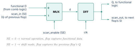
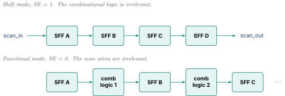
Wire every flop this way, to in a long line, and you get two modes over the same hardware.
3.3 Shift, capture, shift, traced cycle by cycle
Three steps, worth memorizing in this order.
- Assert scan enable and shift in a pattern, taking as many cycles as the chain is long.
- Deassert scan enable and pulse the clock once. This is the capture cycle. The logic evaluates and results land in the flops.
- Assert scan enable and shift out the results while shifting in the next pattern.
Trace a 4-flop chain , loading . The bit destined for must enter first, so the input sequence is .
| Cycle | SE | what happened | |||||
|---|---|---|---|---|---|---|---|
| start | 1 | - | x | x | x | x | unknown state |
| 1 | 1 | 1 | 1 | x | x | x | bit for enters at |
| 2 | 1 | 1 | 1 | 1 | x | x | it moves along |
| 3 | 1 | 0 | 0 | 1 | 1 | x | |
| 4 | 1 | 1 | 1 | 0 | 1 | 1 | pattern loaded |
| 5 | 0 | - | 0 | 1 | 1 | 0 | capture, response latched |
| 6 | 1 | next pat | 1 | 0 | 1 | 1 | unload overlaps next load |
Note cycle 6. Shift-out of this response and shift-in of the next pattern share the same cycles, so a chain of length costs about cycles per pattern rather than .
3.4 The reduction that is the whole point
Without scan, test generation searches over time, hunting a sequence that walks the machine into the right state, exposes the fault, and walks it further until the effect reaches a pin. That search is brutal at real scale. With full scan, every flop output is a controllable primary input and every flop input is an observable primary output, so the circuit under test is no longer a state machine.
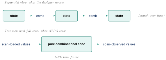
That turns test generation into constraint satisfaction on one snapshot of combinational logic, which is fast and solved. Everything else in DFT is engineering around this reduction. Partial scan was tried and abandoned, since leaving the sequential search partly intact costs more in coverage and tool runtime than it saves in silicon.
3.5 How many chains, worked
with flops, chains, chain length. Take , , MHz.
| Chains | Length | Shift cycles | Test time | Pins needed |
|---|---|---|---|---|
| 1 | 500,000 | 100 s | 2 | |
| 10 | 50,000 | 10 s | 20 | |
| 50 | 10,000 | 2.0 s | 100 | |
| 500 | 1,000 | 0.2 s | 1,000 |
At 5 cents per tester second the one-chain option costs 5 dollars per die, which is absurd. The 500-chain option costs one cent. But a wafer probe card gives perhaps 100 usable signal pins, so a thousand scan pins does not exist. You want the test time of 500 chains and the pin count of 10.
3.6 Compression, and the property that makes it work
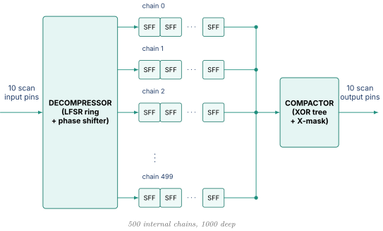
Ten pins obviously cannot carry 500 chains of information. It works because of a property of the patterns, not a trick of hardware. A typical ATPG pattern specifies only 1 to 5 percent of its bits, since detecting one fault constrains only its small logic cone. On 500,000 scan bits, a 2 percent pattern has 10,000 care bits and 490,000 don't-cares. The decompressor is linear over GF(2), so feeding 10 pins for 1,000 cycles injects 10,000 free variables, and the tool solves a linear system for the input sequence producing the required care bits while pseudo-random values fill the rest. Ratios of 10 to 100 are routine.
The compactor's problem is harder and becomes a design constraint. XOR-ing 50 chains means a single X on any one blinds all 50, and X values come from uninitialized arrays, black-boxed blocks, non-scan flops, and bus contention. X-masking shuts off individual chains per pattern, X-tolerant compactors use redundant XOR structures, and underneath both, DFT rules push the RTL to stop producing Xs at all. Aliasing, where two errors cancel in the XOR, is quantifiable and kept far below the DPM budget.
04.Part 4, ATPG
4.1 Activate, propagate, justify
For each target fault the tool does three things, and the three words answer a very common question. Activate the fault by forcing the node to the value opposite the stuck value, so good and faulty circuits differ there. Propagate the difference to an observable point by setting every other input along a path to its non-controlling value. Justify the required values backward to scan flop outputs, which are directly loadable.
Work one. Take , , , and target " stuck-at-0."
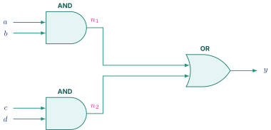
Activate needs in the good circuit, so and . Propagate needs the OR gate's other input at its non-controlling value, so . Justify needs or , so pick both zero. Pattern gives good and faulty . Detected.
Engineers write this in D notation, where means 1 in the good circuit and 0 in the faulty one, so here propagates through the OR to . The classic D-algorithm and PODEM are backtracking searches over exactly these three steps.
The failure case defines a coverage category. If and came from the same upstream signal so forces , activation and propagation demand contradictory things and the fault is untestable. Sometimes that means genuinely redundant logic that could be deleted. Sometimes it means a DFT rule violation you could have avoided. Telling those apart is real work.
4.2 Compaction and the coverage number people argue about
Dynamic compaction works while a pattern is being built, picking another undetected fault and satisfying it with the still-free X bits. Static compaction merges finished patterns whose care bits do not conflict. The result is that 12 million faults ship as 5,000 to 30,000 patterns, because each pattern detects thousands at once, exactly as the AND-gate table showed one pattern catching three.
Two coverage numbers exist and people quote whichever flatters them.
Take 12,000,000 faults, 60,000 untestable by construction, 40,000 undetected because an X blocked observation, 11,900,000 detected.
Half a percent apart, and by the DPM table that is a lot of returned phones. In a review, ask which number is on the slide and what went into the untestable bucket, because "untestable" hides both legitimate redundancy and unfixed rule violations.
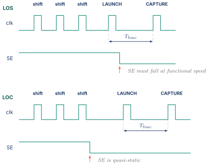
4.3 At-speed, launch-on-capture versus launch-on-shift
Transition faults need two vectors one functional period apart, and there are two ways to make the second.
| Launch-on-shift | Launch-on-capture | |
|---|---|---|
| Second vector is | the shifted pattern, arbitrary | the logic's response to vector 1 |
| ATPG freedom | high | constrained, must justify both |
| Transition coverage | higher by a few percent | a few percent lower |
| Pattern count | lower | higher |
| Scan enable | must switch at functional speed, to every flop | quasi-static |
| Physical cost | a second at-speed high-fanout network, timed like a clock | none extra |
That scan-enable row decides it. Making SE an at-speed signal across 500,000 flops means building a second tree nearly as expensive as the clock tree. LOC is the industry default, with LOS reserved for regions where the coverage gap matters and a local fast SE is affordable.
One more piece of hardware makes at-speed possible at all. A tester cannot push clean 3 GHz edges through a probe card, so fast capture pulses come from the on-chip PLL through an on-chip clock controller, which takes the slow tester clock during shift and gates through a programmable number of fast PLL pulses for capture. The OCC is itself a clock gating structure, which is the bridge to Part 7.
05.Part 5, memory BIST and repair
5.1 Why scan cannot touch an array
An SRAM bitcell is six transistors reached through a word line and bit lines. It is not a flop and has nowhere to put a scan mux. Scanning a 4 Mbit array would need 4 million scan cells, several times larger than the array, defeating the reason the array exists.
Meanwhile arrays are where the defects are. Fifty to seventy percent of the transistors on a modern CPU die are SRAM, drawn with the most aggressive rules on the die, therefore the smallest margins and highest sensitivity to particles and variation. The densest and most defect-prone structure is the one thing scan cannot test. That gap is what MBIST fills. Scan does wrap the array in collar flops so ATPG can test the logic around it, treating the array as a black box producing X, which is one of the main X sources the compactor must handle.
5.2 Array-specific fault models
Arrays fail in ways logic does not. Stuck-at cells. Transition faults, where a cell can be written 0 but not 1, differing from stuck-at because it depends on the previous state. Coupling faults, where an operation on one cell disturbs another, split into inversion coupling that flips the victim, idempotent coupling that forces it to a fixed value, and state coupling that acts only when the aggressor holds a particular value. Address decoder faults, which are logic faults rather than array faults, covering no cell accessed, several cells accessed, or one cell reachable from several addresses. Retention faults, where a cell leaks over milliseconds, needing a deliberate pause that costs expensive tester time. Plus read disturb, write recovery, and sense amplifier imbalance at advanced nodes. The decoder class is the interesting one, because it is why march tests sweep both directions.
5.3 March tests and March C-
A march test is a sequence of march elements, each sweeping the whole address space in a direction and performing a fixed read and write sequence at each address. Notation uses ascending, descending, either. The workhorse is March C-,
costing operations per address, so total.
| Element | What it establishes or catches |
|---|---|
| initializes the array to a known background | |
| every cell held its 0 and can go 0 to 1. Catches sa1 and slow-to-rise | |
| every cell held its 1 and can go 1 to 0. Catches sa0 and slow-to-fall | |
| the same checks with the sweep reversed | |
| final check that nothing was disturbed by the last pass |
The descending elements are not redundant, and this is the detail to be able to explain. A decoder fault mapping address 5 onto the cell for address 6 shows a different symptom depending on whether you visit 5 before 6 or after, so sweeping both directions makes the aggressor-before-victim and victim-before-aggressor orderings both occur.
Runtime. A 32 KB L1 array as 4,096 words gives operations, which at 2 GHz is s. An 8 MB system level cache as 131,072 words gives operations, or s. BIST time is set by the largest array, not the sum, provided each array has its own engine, which is why big arrays are banked with parallel engines. Testing a 64-bit word with solid backgrounds also misses coupling between bits in a word, so real runs sweep several data backgrounds, solid, checkerboard, and stripes, multiplying the time.
5.4 The BIST engine
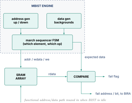
It runs at functional speed, catching speed-sensitive array faults. It needs almost no tester bandwidth, only a start command and a pass or fail bit. And it can re-run in the field at every power-on. The costs are 1 to 3 percent of array area plus the mux on the array's address and data ports, which sits in the functional path exactly as the scan mux does and is not free on a cache whose access time is already critical.
5.5 Built-in self-repair, the biggest lever in DFT
Arrays are built with spare rows and columns, so a 512-row array is physically 514. When BIST finds a failing row, built-in self-repair reprograms the row decoder so the failing address selects a spare. The map lives in eFuses blown at test time and read into repair registers at every power-on, with soft repair into registers available for bring-up.
The yield math is the argument. Model row defects in one array as Poisson with . Without repair an array is bad with probability , so a die with 60 arrays yields
Forty-five percent of dies scrapped for array defects alone, before counting logic defects. Now add two spare rows per array. The array fails only with three or more defective rows, and for small ,
From 55 percent to essentially 100 percent, for two extra rows per array, roughly 0.4 percent area, plus fuses and analysis logic. This is the single highest-leverage piece of hardware in the DFT toolbox, and it is why arrays are the most repairable structures on a chip while random logic is essentially not repairable at all.
BIRA, built-in redundancy analysis, decides the allocation, which is not trivial because one defective cell can be repaired by a row or a column and choosing wrong wastes a spare a later defect needed. Practice identifies must-repair rows and columns first, then searches the remainder.
Note the division of labour with SRAM Arrays and ECC. Repair fixes manufacturing defects once, at test time. ECC fixes soft errors and marginal cells continuously, at run time. You want both, because a cell that is weak rather than dead may pass BIST today and fail in six months at temperature.
06.Part 6, JTAG and the TAP controller
6.1 Boundary scan, the problem it solved
In the 1980s a board was tested with a bed of nails, hundreds of probes physically touching every net. Then ball grid arrays arrived, with connections underneath the package and nothing to touch. The Joint Test Action Group standardized the fix, now IEEE 1149.1. Put a shift register cell at every chip pin, inside the chip, so chips test the board by talking to each other with no probe at all.
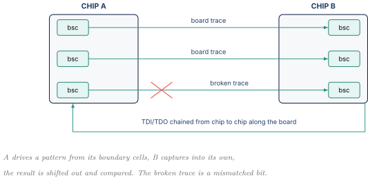
6.2 The TAP state machine
Four mandatory wires plus an optional fifth. TCK test clock, TMS mode select, TDI data in, TDO data out, and optional TRST. All control comes from TMS sampled on the rising edge of TCK, driving a 16-state machine with two nearly identical columns, one for the instruction register and one for a data register.
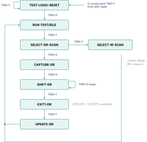
Two facts get asked. Five consecutive TMS=1 cycles force Test-Logic-Reset from any state whatsoever, which is the universal way to a known state and why TRST is optional. And the instruction register selects which data register sits between TDI and TDO, which is how one four-wire port serves dozens of functions. Mandatory instructions are BYPASS, a single flop so a chip can be skipped cheaply in a board chain, IDCODE, a 32-bit identifier that is the first thing any debugger reads because it proves the die is alive, SAMPLE/PRELOAD, and EXTEST for the board test above.
6.3 The modern role, which is not boundary scan
Today JTAG is the universal side door. Private instructions reach the internal scan chains for pattern loading, the MBIST controller for starting tests and reading fail signatures, the fuse controller for repair maps, core debug logic for halting and stepping, trace buffer contents, and through a debug access port the chip's internal bus, so a tool can read and write any memory-mapped register while the chip runs. On ARM SoCs this is the CoreSight DAP, and it is why a debugger can inspect a hung system that is executing nothing.
That power creates the obvious tension. A port that can halt any core and read any register bypasses every software security boundary, so production parts lock it behind debug authentication with a cryptographic challenge, or blow fuses to disable classes of access permanently, with separate levels for secure and non-secure and for invasive versus non-invasive debug. Those levels must be decided before tape-out, since afterward there is no way to add a lock.
07.Part 7, what DFT costs
The difference between someone who has read about scan and someone who has shipped it is entirely in this part.
7.1 Area
A plain D flop occupies 20 to 24 tracks in a modern library, the scan version 24 to 28, so 10 to 20 percent on the flop cell. If flops and their local clock network are 30 percent of block area and scan costs 15 percent on that, the flop contribution is 4.5 percent. Add the decompressor and compactor, the OCC, MBIST engines and collars, spare rows, the fuse array, and chain routing tracks, and total DFT area on a CPU core typically lands at 3 to 8 percent. That is a floorplan line item to declare at the start, not discover at the end.
7.2 Timing on the functional path
The scan mux sits in front of D, lengthening the data path into every capture flop. Work it with the setup equation from Digital Logic and Timing at 2.5 GHz, ps, with , , .
Comfortable. Now insert a 30 ps scan mux ahead of the capture flop.
The path fails. Thirty picoseconds is 7.5 percent of the period, and it lands on every path at once. That is why modern flows insert scan during synthesis rather than as a post-process, so the mux delay is budgeted into every path from the first optimization pass.
A second cost hides in the chain. It connects to flop to flop, and an arbitrary order zigzags wires across the block, causing congestion and, worse, hold violations on the shift path, since a flop-to-flop connection with no logic is precisely the dangerous configuration from section 5.5 of Digital Logic and Timing. Chains are therefore reordered after placement to follow physical proximity, and hold buffers are inserted on the shift path, cells that exist purely for test and leak forever.
7.3 Power, the cost people underestimate
Functional operation toggles maybe 5 to 15 percent of flops per cycle, and gating means the clock reaches only the enabled fraction. Shift mode uses essentially random patterns, so about half of adjacent bits differ, meaning 25 to 50 percent of flops toggle on every shift cycle, and every flop is clocked because gating is bypassed.
Separate out the clock tree, because it is the largest term and the most likely question aimed at you. Suppose dynamic gating suppresses 95 percent of flop clock toggles. Functional clock-tree switching is then 5 percent of ungated. In shift mode every gater is forced transparent, so it is 100 percent.
Twenty times from the gating bypass alone, before the higher data toggling. Total test power three to five times functional is routine.
The consequence is counterintuitive. Large current draw causes IR drop, and the transient at shift start causes droop of the kind in DVFS Droop and Thermal. Lower supply means slower paths, and slower paths mean an at-speed capture can fail. So a perfectly good die that would run real software forever fails the test because of the test, and you scrapped a good part.
| Mitigation | Mechanism | Cost |
|---|---|---|
| Lower shift frequency | shift at 20 to 50 MHz | longer test time, real money |
| Chain grouping | shift a subset at a time | longer test time |
| Low-power ATPG fill | fill don't-cares by repeating the previous bit | more patterns, a little coverage |
| Shift clock gating | gate chains already fully loaded | control complexity |
| Capture staggering | one clock domain captures per pattern | more patterns |
The goal is calibration, not minimization. Test power far below functional means a marginal die passes and fails in the field. Far above means you scrap good dies. The band is set by measurement.
7.4 The clock gating interaction, which you should expect to be asked
A clock gating cell from Power Fundamentals and Clock Gating latches an enable on the low phase and ANDs it with the clock, so a low enable means downstream flops never see an edge. Scan shift needs an edge at every flop every cycle, so every gater must be forced transparent in test. Library ICG cells have a dedicated test enable pin wired so the clock is produced when en | test_enable is true, and DFT rule checking flags any gater whose test pin is unconnected.
Forget it and every flop behind that gater becomes unloadable and unobservable, dropping its whole downstream cone from the coverage number. In a design where you pushed gating to 95 percent efficiency, most flops sit behind a gater, so one misconfigured gater on a wide enable can cost several percent of coverage, which the DPM table prices as very expensive.
Three subtler points separate a correct answer from a good one.
Shift and capture want different things. If test enable is driven only by scan enable, gaters are transparent during shift but behave normally during capture, which is usually what you want for at-speed test because you want the real gating logic exercised. But then ATPG must control the functional enable to get a capture edge where it needs one, so the enable generation logic must itself be reachable from scan. Bury a gater's enable behind a non-scan flop or a hard-coded constant and you create a coverage hole nothing downstream can recover.
The gater is on the clock path, so it makes skew. It delays that branch, so gated and ungated regions see the edge at different times, which is the mechanism from section 6.2 of Digital Logic and Timing. That skew is present in test mode too, and the shift path must meet hold across boundaries where the launch flop is ungated and the capture flop is behind a gater. Shift-mode hold violations across gating boundaries are a real bug class precisely because functional simulation never shows them.
How do you test the gater itself? A gating cell whose enable is stuck at 1 gates nothing. The chip is functionally perfect and burns extra power forever. No functional test finds it, because nothing computes a wrong answer. It is a power defect, not a correctness defect. Catching it needs ATPG explicitly targeting the enable generation logic with the gater output observable, or characterized power measurement compared against expected current for a known pattern. Volunteering this signals you have thought about gating from the test side, not only the design side.
7.5 The rules RTL must follow
Each rule exists for a reason and the reason is the useful part. No internally generated or divided clock reaching a flop without a test mux to a controllable test clock, because ATPG must pulse every flop deterministically. No combinational feedback loops, because a loop has no defined value in a single time frame. No data-path latches unless forced transparent in test, since a latch either blocks the shift or makes its timing level-sensitive. Asynchronous sets and resets forced inactive during shift, because a reset firing mid-shift clears part of the chain and the loaded pattern is garbage, which means a test-mode gate on every async reset in the tree from Clocking Reset and Domain Crossing. Tri-state contention prevention, since ATPG will happily enable two drivers. Bounded X sources, since an X at the compactor blinds a whole XOR group. Special handling for synchronizer flops, usually exclusion from at-speed capture, since a clock domain crossing has no meaningful launch-to-capture timing to test.
08.Part 8, silicon debug is a different discipline
8.1 Where the bug is, versus where the symptom is
DFT answers "is this die manufactured correctly." Silicon debug answers "why does this correctly manufactured die do the wrong thing," which implies a design bug verification missed or a marginality no model predicted.
The defining difficulty is bandwidth. In simulation every signal at every cycle is free and reruns are deterministic. In silicon you have a billion transistors, a hundred pins, and no record. The symptom happened four milliseconds ago, which at 3 GHz is twelve million cycles in the past, and the failure may take twenty minutes to reproduce or may depend on temperature and not reproduce at all.
So debug hardware answers a question with two halves. You cannot bring every signal out, so you must pre-decide which signals. You cannot record forever, so you must pre-decide how to recognize the interesting moment. The second half is harder and it is where triggers live.
8.2 Trace buffers, and the arithmetic that shapes them
A trace buffer is on-die SRAM recording selected signals every cycle into a circular buffer, read out later over JTAG. A buffer of 4,096 entries by 128 bits is 512 Kbit, or 64 KB, comparable to an entire L1 cache and therefore competing with something a customer can measure.
At 3 GHz, 4,096 cycles is s of history. A boot hang two seconds into power-on happened six billion cycles ago. The ratio of what you need to what you can hold is about 1.5 million to one.
Say the conclusion plainly, because it is the sentence that shows you understand the discipline. Buffer depth is nearly irrelevant. The trigger is everything. Doubling the buffer takes 1.37 microseconds to 2.74 against a two-second problem, which is nothing. A trigger that fires on the right cycle turns 4,096 entries into exactly the ones you needed. Secondary techniques stretch effective depth, recording only on qualified events, storing transaction headers rather than payloads, delta encoding slow fields. Each buys a factor of a few. None buys a factor of a million.
8.3 Trigger logic, and this is genuinely your ground
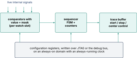
The design points, each a fair follow-up. What you compare against, meaning address ranges rather than exact addresses, transaction IDs, opcode fields, FSM encodings, credit counters hitting zero, queue occupancy thresholds, error flags. Choosing that list is a microarchitecture decision made a year before anyone needs it. Masking, so a trigger fires on a field rather than an exact word. Sequencing, so you can express "A, then B within 200 cycles, then C," which is what turns a trigger from a curiosity into a tool, because interesting bugs are almost always sequences. Counters, to fire on the th occurrence. Cross-triggering, so a condition in one block starts capture in another, which needs a chip-wide trigger bus with a documented latency so the receiver can align its window.
Where the trigger sits in the buffer matters more than it sounds. Trigger-at-start captures forward, trigger-at-end captures the window ending at the event, trigger-at-center does both. Backward is usually what you want, because what you can detect is the symptom and what you need is the cause, which is behind it.
Two costs. The comparator sits on live functional signals, so it is on a real timing path and a wide comparison is a fan-in problem, usually answered by pipelining it and documenting the fixed cycle offset. And the configuration registers must be writable and the data readable when everything else has stopped, which is why debug logic lives on an always-on power domain with an always-running clock. That constraint is exactly what a power controller must provide, which ties this more tightly to your Resource Controller work than it first looks.
Prepare a two-minute account with five parts. What observability gap motivated the triggers. What conditions were programmable and why those. How they were configured and by whom. One concrete bug or bring-up issue they found, with the mechanism. What they cost in area and timing and how you bounded it. An interviewer who reads "built debug triggers" will push for exactly those five things.
8.4 Observability muxes and the debug bus
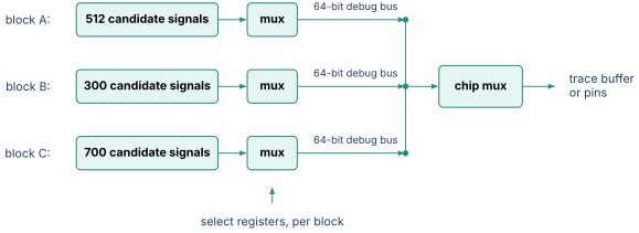
The decision is width against selection granularity. Too narrow, or too coarse, and every debug session becomes five runs with different mux settings, each needing the failure to reproduce. Too wide and you spend wires, muxes, and switching power in every block forever. The rule of thumb is to put control state on the debug bus, not data. Valid and ready handshakes, FSM encodings, credit counts, queue occupancies, arbitration grants, and error flags tell you what the machine was doing. The payload is usually reconstructible from memory and eats the whole width by itself.
8.5 Performance counters
Programmable counters attached to a menu of events, exposed to software. They serve post-silicon validation correlating against the models in Performance Modeling, and software developers tuning real code. The design questions are genuine microarchitecture decisions. How many counters against how many events, since you cannot afford one per event, so four to eight physical counters with a wide event-select field force software to multiplex and sample. Precise against imprecise, since attributing an event to a specific instruction means carrying it to retirement, which costs storage and wiring, but is what a sampling profiler needs to point at a line of code. Speculation accounting, since speculative counts tell you what the hardware did while retired counts tell you what the program needed, and mixing them silently produces confused analysis. Overflow behaviour, including whether it raises an interrupt, which is what makes event-based sampling possible.
Work an example. Measured IPC is 1.2 against a model predicting 1.9. Counters report 12 L2 misses per thousand instructions, 6 branch mispredictions per thousand, and 18 percent of cycles stalled on a full load queue. That triple points at the load path rather than the front end and it took one run. Without counters you have the number 1.2 and no direction. One consequence surprises hardware engineers. Counter definitions become an interface profiling software depends on, so redefining an event between steppings breaks tools in the field.
8.6 Post-silicon bring-up and shmoo plots
Bring-up runs in a standard order. Power on and check current draw, where a gross surprise means a short or a stuck state machine and is caught in the first minutes. Confirm the PLLs lock. Get JTAG responding and read IDCODE, the first real proof the die is alive. Run MBIST and scan, because debugging a design on a defective die wastes weeks. Release reset and execute the first instruction from the boot ROM. Boot to a shell. Run workloads. Characterize.
Characterization produces a shmoo plot, a grid of pass and fail across two swept parameters.
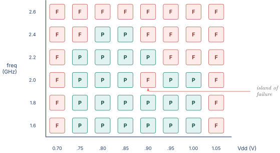
The shape names the mechanism. The diagonal boundary rising to the right is the setup wall, since more voltage makes transistors faster, and it is the curve that defines the DVFS operating points in DVFS Droop and Thermal. The solid F column at 0.70 V across all frequencies is a minimum voltage floor, usually set by SRAM cell stability rather than logic, because a bitcell loses read and write margin before random logic stops switching. Failures at high voltage that vanish lower down are counterintuitive and usually mean a hold or minimum-delay problem, since higher voltage speeds the fast path relative to clock arrival, exactly as in section 5.5 of Digital Logic and Timing. An isolated island in the middle is the nastiest, usually a supply resonance at a specific frequency or a path with non-monotonic behaviour.
One shmoo of one die is an anecdote. Real characterization sweeps temperature and many dies from many wafer positions, producing distributions, and the shipped envelope is guard-banded against the tails.
8.7 Error handling and machine check
Debug hardware helps engineers. Error handling helps the shipped product survive, and it is named explicitly in a power management role.
| Class | Meaning | Response |
|---|---|---|
| Corrected | ECC fixed it, nothing lost | log, count, continue |
| Deferred | data is bad, nobody has consumed it | poison it and defer the decision |
| Uncorrected recoverable | bad data reached a consumer, context known | kill the affected process |
| Uncorrected fatal | machine state untrustworthy | machine check abort, reset |
Poisoning is the idea worth understanding. When a cache line fails ECC the instinct is to raise an error immediately, but maybe nothing ever reads that line, in which case you killed a healthy machine for nothing. Instead the line carries a poison bit through the fabric and the error is raised only when something consumes it, at which point the consumer knows its own context and can often recover locally.
What gets logged is decided long before any error occurs, which is the design lesson. A useful entry has the error type, severity, the address or transaction identifier, the ECC syndrome so you can identify the failing bit and correlate it to a physical array location, a timestamp, and a first-error-sticky bit. That last field is what designers get wrong. Cascading errors are mostly consequences of the first, so a log keeping only the most recent entry describes the wreckage instead of the cause. Keep the first error's full context, set an overflow flag, count the rest. Counting corrected errors over time also predicts degradation, letting software retire pages or schedule a hard repair at the next boot, turning a future crash into maintenance.
09.Part 10, check yourself
Answer out loud, in full sentences, as though an interviewer asked. If you cannot, reread the section named.
- Verification passed ten billion cycles. Explain precisely why that says nothing about a particular die. (1.1)
- Yield is 83 percent and coverage is 99 percent. How many DPM do you ship, and what changes at 99.9 percent? (1.2)
- Give three independent reasons functional test is inadequate for manufacturing test. (1.3)
- The stuck-at model is physically wrong about nearly every real defect. Why does it work anyway? (2.2)
- A die passes the full stuck-at suite and fails in a phone at high clock rates. What did you miss, and what test catches it? (2.3)
- Draw a scan flop, then walk the three-step procedure and say which signal controls which mode. (3.2, 3.3)
- What problem class does full scan reduce test generation to, and why does that matter so much? (3.4)
- You have 500,000 flops and 100 usable test pins. How do you still get the test time of 500 chains, and what property of ATPG patterns allows it? (3.5, 3.6)
- Target " stuck-at-0" in , produce a pattern, and name the three steps as you go. (4.1)
- Compare launch-on-capture and launch-on-shift. Which is the default and what specifically decides it? (4.3)
- Why can scan not test an SRAM array, and why is that the worst possible gap to have? (5.1)
- Write March C-, then explain why the descending elements are not redundant. (5.3)
- Sixty arrays, one percent per-array defect rate. Compute yield with and without two spare rows, and say why BISR is the biggest lever in DFT. (5.5)
- You drove clock gating to 95 percent. What happens to shift-mode clock power, and what must be done to every gater before scan works at all? (7.3, 7.4)
- How would you detect a clock gater whose enable is stuck at 1? (7.4)
- Your trace buffer holds 4,096 cycles and the bug appears two seconds into boot. What does that ratio tell you about where to spend design effort? (8.2, 8.3)
- A shmoo fails only at high voltage. What mechanism do you suspect and why? (8.6)
- Errors are cascading and your log keeps only the most recent. What did you get wrong and what is the fix? (8.7)
10.Part 11, related notes
- SRAM Arrays and ECC for the arrays MBIST tests, the spare rows BISR consumes, and the runtime ECC that complements manufacturing repair
- Power Fundamentals and Clock Gating for the gating cells that must be test-bypassed, which is your most likely crossover question
- STA Synthesis and Physical Design for where scan insertion sits in the flow and the chain reordering step
- Digital Logic and Timing for the setup and hold equations reused in 7.2 and the skew behind shift-mode hold failures
- Clocking Reset and Domain Crossing for the reset gating and synchronizer exclusions the DFT rules demand
- DVFS Droop and Thermal for the droop test power causes and the operating envelope the shmoo defines
- Performance Modeling for what performance counters get correlated against
- SoC Integration and Interfaces for DFT as an integration contract item and JTAG access across the SoC
- Verification Methodology for the discipline that finds design bugs, which is what this note explicitly is not