Synthesis, Static Timing Analysis, and Physical Design
September 8, 202665 min readadvanced
Four lines. Now list what is missing before this can be manufactured. There is no adder, because + is an operator and not a circuit, and Arithmetic Hardware gives at least six adder structures with different…
01.Part 1, what the tool is actually being asked to do
1.1 The gap between what you write and what gets built
Start with something small enough to hold in your head.
| always_ff @(posedge clk) begin | |
| if (en) sum_q <= a + b; | |
| end |
Four lines. Now list what is missing before this can be manufactured. There is no adder, because + is an operator and not a circuit, and Arithmetic Hardware gives at least six adder structures with different area and delay. There are no flip-flops, because sum_q is a name and not a device. There is no clock gating cell even though en is exactly the enable an ICG wants, per Power Fundamentals and Clock Gating. Nothing decides how strongly sum_q drives its readers, or whether the adder should be small and slow or large and fast.
Every one of those is a choice, and every choice trades area against delay against power. Synthesis is a search over an enormous space of physically buildable circuits, all computing the same function, looking for the one that best fits constraints you supply.
Count the space once so "enormous" means something. Suppose the adder can be built five ways, each flop comes in six drive strengths and three threshold voltages, and there are eight flops. Ignoring everything else, that is netlists for four lines of RTL, and a real block has two million instances. No tool searches that. Every synthesis tool is a pile of greedy heuristics that make a locally good move, measure, and move again, which explains most of its apparently strange behavior. It is not reasoning about your design. It is hill-climbing on a cost function you wrote.
1.2 The library, which is where delay actually lives
Before anything can be optimized the tool must know what a gate costs. That lives in the standard cell library, delivered as a .lib file, and its shape kills a family of misconceptions.
The naive belief is that an AND gate has a delay, some fixed number of picoseconds. It does not. From Digital Logic and Timing, delay is the time to move charge onto a capacitance, so it depends on how much capacitance the gate drives. It also depends on something less obvious, which is how fast its own input arrived, because a lazily rising input keeps the transistors partly off for longer. So the library stores delay as a two-dimensional table indexed by input transition time and output load. This is the non-linear delay model, or NLDM.
A plausible table for a small inverter, delays in picoseconds.
| input slew \ output load | 1 fF | 4 fF | 16 fF |
|---|---|---|---|
| 10 ps | 8 | 18 | 58 |
| 40 ps | 14 | 24 | 64 |
| 160 ps | 38 | 48 | 88 |
Work an entry the tool would actually need. Your inverter sees a 25 ps input transition and drives 8 fF, which is not in the table, so it interpolates. At 10 ps slew, between 4 fF giving 18 and 16 fF giving 58, at 8 fF you get ps. At 40 ps slew the same step gives ps. Interpolating between those at 25 ps, halfway between 10 and 40, gives ps.
Two facts fall out and both matter later. Load dominates. Going from 1 fF to 16 fF at fixed slew takes delay from 8 to 58 ps. Fit a line and you get with in fF, which is the familiar intrinsic delay plus drive resistance times load. Slew is contagious. At 4 fF, a 10 ps input slew gives 18 ps of delay and a 160 ps input slew gives 48 ps. The same gate driving the same load is 30 ps slower purely because its input was lazy, and its own output will be lazy too, which slows the next gate. Bad slew compounds along a chain, which is why a constraint exists to stop it in 3.4.
The library also holds setup and hold times per flop, again as tables, plus area, leakage per state, and internal switching energy per transition. When somebody says "the library," this is the object.
1.3 Constraints are the cost function, and the tool has no other opinion
The tool can build many circuits and price each one. What it cannot do is decide what "better" means. That comes from you, as constraints, and this sentence governs everything through Part 7.
Synthesis optimizes what you constrain. An unconstrained path is not optimized at all. A wrongly constrained path is optimized enthusiastically toward the wrong goal.
Say it a second way, because people nod and then forget. The tool is not trying to make your design good. It is trying to reduce numbers in a report. A path not in the report gives it no reason to act, and it will happily leave that path ten times slower than everything around it. A path in the report with the wrong number attached gets unlimited area and power spent dragging it toward a target that corresponds to nothing real.
Nearly every complaint of the form "the tool did something stupid" is a constraint problem. Learning to suspect your own SDC before you suspect the tool is most of what separates somebody who has closed timing from somebody who has read about it.
02.Part 2, synthesis in three phases
2.1 Elaboration, from text to a graph
Elaboration turns source text into a data structure. It resolves parameters, so parameter WIDTH = 32 becomes the literal 32. It unrolls generate blocks and static for loops into actual instances with distinct names. It builds hierarchy, connects ports, and resolves which module each instantiation refers to. Then it infers hardware from behavior, so an always_ff @(posedge clk) becomes generic flip-flops, an always_comb becomes a generic combinational cone, and a + becomes a generic adder operator with no structure yet. This is where inferred latch warnings come from, per RTL Design and SystemVerilog, because an always_comb with an incomplete assignment leaves a signal needing to hold its old value and only a latch does that.
The output is technology-independent, holding abstract adders and muxes and flops with no knowledge of which library will implement them, and that independence is deliberate since the same elaborated design can then map to a 5 nm library or an FPGA. Elaboration is also where your RTL bugs stop being your RTL bugs, because after this the tool reasons about a graph and its messages point at instance names you never wrote.
2.2 Logic optimization, working on the abstract graph
Boolean minimization. Take , three ANDs and two ORs as written.
| 0 | 0 | 0 | 0 | 0 | 0 | 0 | 0 |
| 0 | 0 | 1 | 0 | 1 | 0 | 1 | 1 |
| 0 | 1 | 0 | 0 | 0 | 0 | 0 | 0 |
| 0 | 1 | 1 | 0 | 1 | 1 | 1 | 1 |
| 1 | 0 | 0 | 0 | 0 | 0 | 0 | 0 |
| 1 | 0 | 1 | 0 | 0 | 0 | 0 | 0 |
| 1 | 1 | 0 | 1 | 0 | 0 | 1 | 1 |
| 1 | 1 | 1 | 1 | 0 | 1 | 1 | 1 |
The last two columns match in all eight rows, so is redundant and five gates become three. The reason not to do this by hand in RTL is that the tool does it perfectly on functions of forty inputs where no human sees the pattern.
Resource sharing, and why it is a tradeoff and not a win.
| always_comb begin | |
| if (sel) y = a + b; | |
| else y = c + d; | |
| end |
Read literally that is two 32-bit adders and one 32-bit output mux. Call a 32-bit adder about 200 gate-equivalents and a 32-bit 2-to-1 mux about 64, so the literal version is GE. Only one result is ever used, so the tool can mux the inputs and share one adder, giving GE. A 29 percent saving.
Now the catch, which is 1.3 in miniature. The shared version puts a mux in front of the adder, so the critical path grew by roughly 30 ps. If the path had 200 ps of slack, sharing is free area. If the path was critical, sharing just cost frequency. The tool decides from the timing constraint you gave it. Constrain it tightly and the tool refuses to share and builds two adders. Leave it unconstrained and the tool shares aggressively and you find out at signoff. Same RTL, opposite netlists, one line of SDC between them.
The tool also rebalances expression trees, so at depth three becomes at depth two, propagates constants, merges common subexpressions, and deletes logic that cannot reach any output.
2.3 Technology mapping, and the optimization that never stops
Technology mapping replaces generic operators with real cells. The generic adder becomes a specific structure chosen from what the library offers and what the timing demands, so a slack-rich path gets a compact ripple-carry and a critical path gets a Kogge-Stone at three times the area. Covering is not one-to-one, because a library has complex cells like AOI21 and OAI22 implementing two-level functions in one cell more cheaply than the gates they replace.
Then the tool keeps optimizing, which is where most of the runtime goes. Sizing picks among INVX1 through INVX16, trading area, leakage, and the capacitance presented to the upstream driver, which is why sizing is never a local decision. Buffering inserts chains to restore slew and trees to split fanout. Cloning duplicates a cell driving thirty loads so one copy serves the three on the critical path and the other serves the twenty-seven that do not matter. Threshold swapping puts low-Vt on critical paths and high-Vt everywhere with slack, and from Power Fundamentals and Clock Gating that means over 80 percent of a typical block ends up high-Vt leaking a tenth as much. Path restructuring pulls late-arriving inputs closer to the output, so a signal arriving 200 ps after its neighbors passes through one gate instead of three.
2.4 A synthesis sweep, which is what PPA reasoning actually looks like
The abstract claim is that power, performance, and area trade against each other. Here is that as numbers. One block, synthesized repeatedly at tightening target periods, changing nothing but create_clock.
| Target period | Achieved | Area (kGE) | Dynamic power | Leakage | What the tool did |
|---|---|---|---|---|---|
| 1.20 ns | 1.20 ns | 42 | 18 mW | 1.2 mW | minimum sizes, all high-Vt, heavy sharing |
| 1.00 ns | 1.00 ns | 48 | 24 mW | 1.5 mW | some upsizing, less sharing |
| 0.90 ns | 0.90 ns | 58 | 32 mW | 2.8 mW | low-Vt on critical paths, adders restructured |
| 0.85 ns | 0.85 ns | 76 | 45 mW | 6.1 mW | heavy low-Vt, cloning, duplicated logic |
| 0.80 ns | 0.83 ns | 94 | 58 mW | 9.4 mW | target missed, area and power spent anyway |
Price a picosecond as you move down. From 1.20 to 1.00 you bought 200 ps for 6 kGE, or 30 GE per picosecond. From 0.90 to 0.85 you bought 50 ps for 18 kGE, or 360 GE per picosecond. Twelve times more expensive for the same picosecond. The curve is convex and has a knee, and the engineering decision is to sit at the knee.
The last row is the lesson people learn the hard way. Asking for 0.80 ns produced 0.83 ns and burned 18 kGE and 13 mW getting there, and worse, the tool spent its whole effort budget on paths it could never close while neglecting paths that were merely close. Over-constraining is not free insurance. Constraining 5 to 10 percent tight so that degradation through place and route lands you on target is defensible. Constraining 30 percent past what the design can do is self-harm.
03.Part 3, SDC, the contract between you and the tool
Synopsys Design Constraints is the standard format and is really Tcl, which is why Programming and Tooling cares about Tcl. Every implementation and analysis tool reads the same SDC, so it is the single source of timing intent. The syntax is easy. The concepts are what get asked.
3.1 create_clock, which is where comes from
| create_clock -name clk -period 1.000 [get_ports clk] |
That line establishes ns, exactly the in the setup equation from Digital Logic and Timing.
Without it there is no , so no setup check, so nothing in the design is timed at all. A missing or mistyped create_clock is the most catastrophic SDC error available, and its signature is a run that finishes fast and reports beautiful timing on a design that will not work.
A generated clock is one derived inside the design, such as a divider output, a gated clock, or a clock mux output.
| create_generated_clock -name clk_div2 -source [get_ports clk] -divide_by 2 [get_pins div_reg/Q] |
You declare it rather than letting the tool guess, because the tool needs the relationship between the two clocks to time paths crossing between them. A forgotten divided clock means that domain gets timed against the fast clock and over-constrained, or gets treated as unclocked and not timed at all. A virtual clock has no port in this design and exists purely as the reference for the input and output delays of 3.3.
3.2 Ideal clocks, propagated clocks, and set_clock_uncertainty
Before clock tree synthesis in 8.4 the tree does not exist. No buffers, no wires, no branch points. The tool treats the clock as ideal, arriving everywhere at the same instant with zero delay. That is false, and the placeholder standing in for the falsehood is uncertainty.
| set_clock_uncertainty -setup 0.080 [get_clocks clk] | |
| set_clock_uncertainty -hold 0.030 [get_clocks clk] |
Uncertainty is subtracted from the time available for setup and added to the time required for hold. Decompose it rather than treating it as one number. Pre-CTS, 80 ps of setup uncertainty might be 40 ps of estimated skew, 25 ps of jitter, and 15 ps of general margin.
After CTS the tree is real, so you switch to propagated and the tool computes the actual arrival at every flop from the actual buffers and wires.
| set_propagated_clock [get_clocks clk] | |
| set_clock_uncertainty -setup 0.040 [get_clocks clk] |
Skew is now computed per path rather than guessed, so it must come out of the uncertainty number. Forget that and you count skew twice, over-constraining every path in the design by 40 ps. On a 1 ns period that is four percent of frequency thrown away, paid for in area and leakage across the whole block, and completely invisible unless somebody reads the SDC.
Setup and hold uncertainty differ and should. Jitter is a variation between two different clock edges, so it hurts setup, where launch and capture are different edges. For a same-clock hold check, launch and capture are the same edge, so that edge's jitter is common to both sides and largely cancels. Hold uncertainty is therefore smaller and covers skew estimate and modelling margin rather than jitter.
3.3 Input and output delay, and the bug that finds you three months later
This separates people who have integrated a block from people who have only synthesized one.
You are handed a block with an input port data_in and an output port data_out. How much of the clock period does the logic inside your block get?
The instinct is "all of it." Here is why that is wrong.
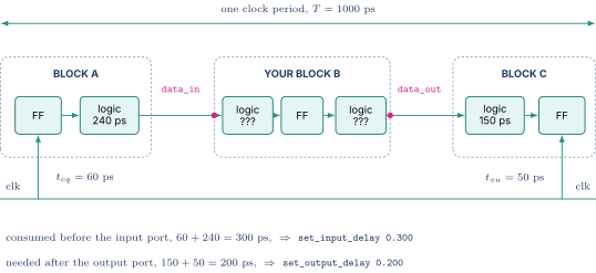
The flop launching data_in lives in block A. It burns 60 ps of clock-to-Q then 240 ps of block A's logic before the signal reaches your port, so 300 ps of the period is gone before you see it. Symmetrically the value you drive out must cross 150 ps of block C's logic and satisfy 50 ps of setup there, so 200 ps must remain after your port.
| set_input_delay 0.300 -clock clk [get_ports data_in] | |
| set_output_delay 0.200 -clock clk [get_ports data_out] |
Now the budget. For a path from data_in to your first internal flop, with 40 ps of internal setup and 80 ps of uncertainty,
580 ps of logic depth, not 1000. This is the answer to "why can a block not be timed in isolation." A block is one segment of a path that begins and ends in other people's flops, and STA needs the whole path. Input and output delay describe the part you cannot see.
The loud failure mode. Leave out set_input_delay. The tool assumes zero and believes the budget is ps. Synthesis builds 860 ps of logic, reports +20 ps of slack, and everyone declares victory. Three months later at integration the real arrival is 300 ps later, so the path is ps against 1000. Slack is -280 ps, and the fix is an RTL restructuring in a block signed off a quarter ago, by a team that has moved on, against a tapeout date that has not.
The quiet failure mode. Set input delay to 600 ps when it is really 300. The tool now believes it has 280 ps and goes to war, upsizing everything, swapping in low-Vt cells that leak ten times more, duplicating logic, possibly demanding an extra pipeline stage. The block closes, nobody complains, and you shipped an oversized power-hungry block solving a problem that did not exist. Nobody ever finds this, because a design that closes timing does not get audited.
These two numbers are a negotiation between block owners, usually managed by a chip-level budget spreadsheet, and being wrong in either direction costs real money.
3.4 The electrical constraints, which exist for reasons
| set_max_transition 0.150 [current_design] | |
| set_max_capacitance 0.100 [current_design] | |
| set_max_fanout 24 [current_design] | |
| set_driving_cell -lib_cell BUFX4 [all_inputs] | |
| set_load 0.050 [all_outputs] |
set_max_transition caps how slow any edge may be, and three separate things break without it. The NLDM tables in 1.2 are characterized only out to some maximum slew, so beyond it the tool extrapolates and the delay numbers are fiction. Short-circuit power from Power Fundamentals and Clock Gating is proportional to input slew, so lazy edges burn crossover current in every receiving gate. And a slow edge lingers in the region where a neighboring aggressor can couple onto it and cause a noise failure. A design without a slew constraint has a timing report that cannot be believed. set_max_capacitance and set_max_fanout cap the cause rather than the symptom. set_driving_cell tells the tool what drives your input ports, since the arriving slew depends on the external driver, and without it the tool assumes an infinitely strong driver with an instant edge and under-estimates your input paths. set_load tells it what your outputs drive.
One more command is underused. set_case_analysis 0 [get_ports scan_mode] declares a signal constant for this analysis, and the tool then propagates that constant and automatically stops timing everything it disables. That is structurally safer than hand-writing false paths, because the tool derives the consequences instead of trusting you to enumerate them.
04.Part 4, timing exceptions
4.1 The default, so you can see what an exception departs from
Every STA tool assumes, unless told otherwise, that data launched by one clock edge must be captured by the very next edge of the capture clock. One period. Every path. That default is right for the overwhelming majority of paths and is why STA works at all. A timing exception is a statement that some path does not obey it.
4.2 False paths, meaning paths whose timing cannot cause a failure
A false path is one the tool should not check at all. Not a path that is fast. A path whose arrival time cannot produce a wrong answer.
A properly synchronized clock domain crossing. A signal leaves a flop on clk_a at 800 MHz and lands on the first flop of a two-flop synchronizer on clk_b at 1.1 GHz. From Clocking Reset and Domain Crossing the clocks have no fixed phase relationship, so the tool finds the worst possible alignment of the two edges and reports a huge violation. But the design already accepts that this flop will sometimes go metastable, which is exactly what the second flop is for. The check is not merely hard to meet, it is meaningless, because no arrival time makes it pass and no arrival time makes the design incorrect.
| set_clock_groups -asynchronous -group {clk_a} -group {clk_b} |
Prefer set_clock_groups -asynchronous over hand-written false paths between domains. It is symmetric, covers both directions and every path, and cannot be half-written. A hand-written set covering clk_a to clk_b but forgetting the reverse leaves half the crossing over-constrained, burning area fighting a path that does not exist. The critical caveat is that declaring it false removes the timing check and nothing else. The CDC structural check of 9.6 is what proves a synchronizer is actually there. A false path across an unsynchronized crossing is not an exception, it is a silenced alarm on a real bug.
A test-mode-only path. Scan chains from DFT and Silicon Debug shift at maybe 20 MHz while the functional clock runs at 1 GHz, so timing the scan path at 1 GHz checks a configuration that never occurs. Better than a false path, use set_case_analysis on the scan enable so the tool works out which paths are disabled, then analyse shift mode separately at its own clock as one of the modes in 6.3.
Logically exclusive paths. Two signals feed a mux under conditions that cannot both be true, so a path through both is structurally present and functionally impossible. This is where false paths get dangerous, because "these can never both be true" is an assertion about your design that should have been proved with formal per Verification Methodology rather than asserted in a constraint file.
4.3 Multi-cycle paths, and the classic error
A multi-cycle path is genuinely allowed more than one period. The canonical case is a slow arithmetic unit whose consumer is designed to wait.
Clock at 2 GHz, so ps. The multiplier's combinational delay is 850 ps, ps, ps, ps, and the fast-corner minimum path through it is 300 ps with ps. The consumer's enable fires every second cycle, so the result is genuinely not needed for two cycles.
Default check. Required 500 ps, needed ps, slack ps. Unfixable by any amount of sizing.
Declare the setup multicycle.
| set_multicycle_path 2 -setup -from [get_pins mul_a_reg*/CK] -to [get_pins mul_q_reg*/D] |
The setup capture edge moves from 500 to 1000 ps, and slack becomes ps. Closed.
Now the trap. The hold check does not stay put. The hold capture edge is defined as one edge before the setup capture edge, so moving setup to edge 2 drags hold to edge 1.
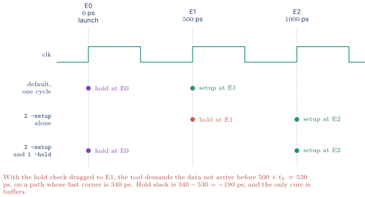
The tool fixes that the only way hold is ever fixed, by inserting delay, and 190 ps of delay on all 64 bits of a multiplier output is hundreds of buffers, tens of thousands of square microns, and milliwatts of leakage. In a flow without auto-fix it is instead a wall of hold violations nobody can explain.
| set_multicycle_path 1 -hold -from [get_pins mul_a_reg*/CK] -to [get_pins mul_q_reg*/D] |
The rule to memorize is -hold gets when -setup gets , for a same-clock multicycle. Write both or write neither.
And the part that matters more than the arithmetic. A multi-cycle path is a claim about your design, not a hint to the tool. The claim is that the capture flop does not sample on the intermediate edge and that the launch value is held stable across the whole window, and usually both come from the same enable. If that enable is wrong, or if somebody later changes the control logic so the flop captures every cycle, the SDC still says two cycles and the tool still allows 960 ps of logic, and at edge 1 the destination samples a half-settled value. That is a functional bug, it is in silicon, and no timing report will ever show it, because you told the tool not to look. Multi-cycle paths belong in a reviewed list with a written justification per entry, and the justification is what to check, not the syntax.
4.4 Max delay and min delay
| set_max_delay 0.400 -from [get_ports async_req] -to [get_pins sync1_reg/D] | |
| set_min_delay 0.100 -from [get_pins a_reg/CK] -to [get_pins b_reg/D] |
These set explicit bounds where the clock-relationship machinery does not apply. The common legitimate use is a crossing already declared asynchronous where you still need to bound the skew between the bits of a multi-bit bus, or bound total delay so a pulse does not get stretched or a signal does not arrive so late that a downstream synchronizer sees it in the wrong cycle. Declaring a crossing false removes all control over how long it takes, and sometimes you need some.
4.5 The symmetric danger, which is the interview point
| Consequence | When you find out | Cost | |
|---|---|---|---|
| Missing exception | tool over-optimizes a path that did not matter | never, unless somebody audits | area, power, leakage, and effort stolen from paths that did matter |
| Wrong exception | tool ignores a path that did matter | in silicon, on a workload nobody simulated | respin |
A missing exception is expensive. A wrong exception is fatal. The asymmetry is unpleasant because the expensive one is invisible and the fatal one is easy to write. Every exception is an unproven assertion about the design, and mature flows treat the exception list the way they treat a waiver list, with an owner and a reason per line.
05.Part 5, static timing analysis proper
5.1 Why static replaced dynamic
Before STA you verified timing by simulating with delays annotated on every gate, which still has a narrow role per Verification Methodology. The problem is coverage. To catch a setup violation in simulation you must stimulate the path, meaning find an input vector that toggles it and propagates the transition all the way to the endpoint. For the ripple-carry adder in Digital Logic and Timing the critical path only activates for inputs generating a carry all the way up. Finding a vector for one path is a puzzle. Finding vectors for all ten million paths in a block hits the same combinatorial wall as Part 1 of Verification Methodology.
STA does not simulate. It walks the graph, propagating arrival times forward from every startpoint and required times backward from every endpoint, taking the worst combination at every node. It never needs a vector because it never needs to know what value is on a wire, only how long a transition takes to get there, so it is exhaustive over paths by construction and runs in minutes. The price is that STA is pessimistic, reporting paths no vector can activate, which is exactly the false-path problem of 4.2. It trades false alarms for completeness, and that is the right trade, because a false alarm costs an afternoon and a missed violation costs a respin.
5.2 Timing paths, startpoints, endpoints, and the four groups
A timing path runs from a startpoint to an endpoint through combinational logic only. A startpoint is a sequential element's clock pin or a design input port. An endpoint is a sequential element's data pin or an output port. Every path has one of each and contains no sequential element between, which is why a path never crosses a flop.
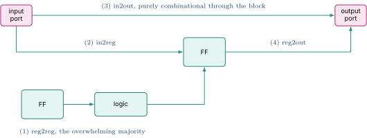
reg2reg is usually 95 percent or more of a block's paths and is fully under your control, since both ends are yours. in2reg and reg2out depend on the input and output delays of 3.3, so their slack is only as trustworthy as those numbers. in2out passes straight through with no flop, which is often a design smell, since combinational feedthrough forces neighbors to budget around you.
Two more checks live alongside these and get forgotten. Clock gating checks verify the enable into an ICG arrives in time relative to the clock, which is the negative-skew problem in section 4.2 of Power Fundamentals and Clock Gating. Recovery and removal are the setup and hold equivalents for asynchronous reset de-assertion, per Clocking Reset and Domain Crossing.
5.3 Arrival, required, and slack, worked all the way through
Everything reduces to three numbers per endpoint. Arrival time is when the signal actually gets there. Required time is the latest it could have arrived and still worked. Slack is required minus arrival.
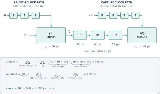
Read the required line carefully, because the sign of every term is the point. The capture edge happens one period after launch, so . That edge takes 345 ps to reach FF2's clock pin, so the useful deadline is 345 ps later still. Uncertainty is margin held back, so it is subtracted. Setup is the window the flop needs before its edge, so it is subtracted.
Notice something the two-flop picture in Digital Logic and Timing hides. The launch clock path is 320 ps and the capture path is 345 ps, so FF2's edge arrives 25 ps later. That is skew, ps, and it appears here not as a separate term but as the difference between two clock network numbers. It added 25 ps to the setup budget and it will subtract 25 ps from the hold budget, exactly as section 6.2 of Digital Logic and Timing says. STA never uses the skew equation. It computes both clock paths independently and the arithmetic produces the same answer.
5.4 Reading a real timing report
  Startpoint: FF1     Endpoint: FF2     Path Group: clk    Path Type: max

  Point                                    Incr       Path
  ---------------------------------------------------------------
  clock clk (rise edge)                    0.000      0.000
  clock network delay (propagated)         0.320      0.320
  FF1/CK (DFFX1)                           0.000      0.320  r
  FF1/Q (DFFX1)                            0.060      0.380  f
  n12 (net, fanout 3)                      0.010      0.390  f
  U1/Z (AND2X1)                            0.045      0.435  f
  n13 (net, fanout 1)                      0.010      0.445  f
  U2/Z (XOR2X2)                            0.080      0.525  r
  n14 (net, fanout 6)                      0.010      0.535  r
  U3/Z (OAI21X1)                           0.055      0.590  f
  FF2/D (DFFX1)                            0.000      0.590  f
  data arrival time                                   0.590
  ---------------------------------------------------------------
  clock clk (rise edge)                    0.500      0.500
  clock network delay (propagated)         0.345      0.845
  clock uncertainty                       -0.040      0.805
  FF2/CK (DFFX1)                           0.000      0.805  r
  library setup time                      -0.045      0.760
  data required time                                  0.760
  ---------------------------------------------------------------
  slack (MET)                                         0.170
Three habits make this useful rather than decorative. Watch the fanout column, since n14 at fanout 6 is a cloning candidate if that 10 ps is really 40 ps in the failing version. Watch the cell types, since a long run of X1 cells on a critical path means the tool never sized them, which usually means the path became critical late. And compare the two clock network numbers, since a large difference is skew, and an unintended skew is a CTS problem that no amount of RTL restructuring will fix.
5.5 WNS, TNS, and reading the histogram
Worst negative slack is the single most negative slack. Total negative slack is the sum over all failing endpoints. WNS says how far from closing you are. TNS says how much of the design is involved. You need both, and the reason is best seen as a picture.
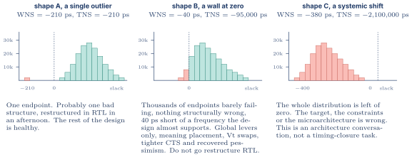
Three shapes, three completely different responses, and a report quoting only WNS cannot distinguish B from C. Ask for both numbers and, if you can, the histogram. Saying "we were at -40 ps WNS with 95 nanoseconds of TNS across 3,200 endpoints" tells a listener immediately that you were in shape B and were not going to fix it with an RTL change.
5.6 Slew, the third number the tool is tracking
Reports quote arrival and slack, but the tool also carries a transition time at every node, being how long the signal takes to swing between the 10 and 90 percent points of the rail. Slew matters because of 1.2, since a gate's delay depends on its input slew, so slew must propagate alongside arrival time. A cell driving a big load produces a slow edge, which slows the next cell, which produces an even slower edge if it is also loaded, so slew degrades along a chain and a path that looks eight gates deep ends up with the delay of twelve.
This is why violations of set_max_transition are reported as design rule violations that the tool fixes before it fixes timing. A DRV invalidates the delay numbers, so there is no point optimizing timing computed from slews outside the characterized range. The order in every implementation tool is DRV, then setup, then hold.
06.Part 6, corners, modes, and variation
6.1 One cell, many behaviors
Three things outside your run-time control set a transistor's speed.
Process. Manufacturing varies wafer to wafer, die to die, and across one die. The foundry characterizes at named corners, so SS is slow-NMOS slow-PMOS, FF is fast-fast, TT is typical, and the mixed SF and FS matter wherever a rising edge races a falling one.
Voltage. Delay depends on the overdrive . Less supply, less current, slower gate. A block at 0.9 V nominal is characterized at 0.81 V and 0.99 V for a ten percent tolerance, and if it does DVFS per DVFS Droop and Thermal then every operating voltage is its own corner.
Temperature. Higher temperature reduces carrier mobility, making transistors slower, and raises leakage steeply per Power Fundamentals and Clock Gating.
The standard rule is that setup is worst at the slow corner, meaning slow process, low voltage, and high temperature, because all three lengthen the data path and setup is a race against the period.
Now the counterintuitive part, worth volunteering. Temperature has two competing effects. Mobility falls as temperature rises, which slows the device. But threshold voltage also falls as temperature rises, which raises the overdrive and speeds it up. At high supply the mobility term dominates and hot is slow, which is where the classical rule comes from. At low supply, which is exactly where a modern low-power design lives, the threshold term dominates and cold becomes the slow case. That is temperature inversion, and its consequence is that you cannot just check the hot corner. Modern signoff checks both temperature extremes at every voltage, which is one reason the corner count in 6.3 got so large.
6.2 Why the fast corner is worst for hold
Hold fails when data arrives too early. The fast corner, meaning fast process, high voltage, low temperature, is where every gate is quickest, so it is where data arrives earliest and hold is most likely to fail. Setup and hold are therefore checked at opposite corners, and this is not a formality, since a design can pass setup at SS and pass hold at FF and still fail if you ran only one.
There is a second reason the fast corner is nastier than it looks. From 5.3, positive skew hurts hold, and at the fast corner the clock tree branches do not speed up uniformly, so skew can grow in absolute terms in places. Hold failures at the fast corner are frequently clock-tree failures wearing a datapath costume.
A useful summary. Setup is a slow-corner problem and a performance problem. Hold is a fast-corner problem and a functional problem.
6.3 Multi-corner multi-mode, and counting how bad it gets
A corner is a PVT combination plus an RC extraction condition. A mode is a functional configuration with its own SDC, such as normal operation, scan shift, scan capture, at-speed test, retention, or each DVFS operating point.
| Axis | Values | Count |
|---|---|---|
| Process | SS, TT, FF | 3 |
| Voltage | 0.75 V, 0.90 V, 1.05 V from the DVFS table | 3 |
| Temperature | -40 C and 125 C, both needed because of temperature inversion | 2 |
| RC corner | Cmin, Cmax | 2 |
| Mode | functional, scan shift, scan capture, at-speed test | 4 |
Naively scenarios. In practice flows prune to a signoff list of 20 to 40 covering the space, since many combinations are impossible or provably dominated. But each is a full analysis over hundreds of thousands of endpoints, and a fix helping one scenario can hurt another. This is where timing closure stops being an equation and becomes a project.
Two consequences. An ECO fixing setup at SS by adding delay can create a hold failure at FF, so every fix is re-checked across the whole list rather than the one scenario that reported it. And runtime and disk become engineering constraints, which is why flows analyse all scenarios concurrently in one tool session rather than running 30 independent jobs.
6.4 On-chip variation, derating, and where the pessimism comes from
Within-die variation is the fact that two nominally identical cells on the same die, made on the same wafer in the same second, are not identical, because random dopant fluctuation, line-edge roughness, and local stress all differ micron by micron. A corner captures die-to-die variation. Nothing so far captures cell-to-cell variation within one die.
The crude fix is derating, a multiplier making the launch path slow and the capture path fast so you get the worst combination.
| set_timing_derate -late 1.05 -cell_delay | |
| set_timing_derate -early 0.95 -cell_delay |
Safe, simple, and badly pessimistic for two separate reasons.
Reason one, common path pessimism. In the report of 5.4, the launch clock path is 320 ps and the capture path is 345 ps, and those are not independent. They share the first several buffers before the tree branches, so suppose 280 ps of both numbers is literally the same physical buffers driving the same physical wires. Blanket derating makes those buffers 5 percent slow in one calculation and 5 percent fast in the other, asserting that one buffer is simultaneously slow and fast. That is not conservatism, it is nonsense. Common path pessimism removal credits it back.
Twenty-eight picoseconds recovered on this path for free, by declining to believe something impossible. On a 500 ps period that is 5.6 percent of the cycle.
Reason two, and this is the good one, is that random variation averages out over path depth. Suppose each stage's delay has a random component with standard deviation about a mean . A path of stages has total mean , and because the per-stage variations are independent the total standard deviation is rather than . So the relative variation of the path is
Work it. Take a single-stage relative variation of 8 percent. A 20-stage path has relative variation percent. A blanket derate applies the single-stage 8 percent to the whole path, so on a 400 ps path it holds back 32 ps of margin when the justified figure is 7 ps. Twenty-five picoseconds thrown away, on every deep path in the design.
That derivation is the entire justification for advanced OCV and parametric OCV. AOCV replaces the single factor with a table indexed by path depth and by the physical distance the path spans, since a path spread across a millimetre sees more systematic variation than one packed into a corner. POCV goes further, carrying a mean and a standard deviation per cell, combining them statistically along the path, and reporting slack at a chosen sigma level, typically three sigma.
The direction surprises people, so state it plainly. Short paths get derated more than long paths, not less. A two-stage path has relative variation, so 5.7 percent, against 1.8 percent for twenty stages. Blanket derate is optimistic for short paths and pessimistic for deep ones, and short paths are exactly where hold checks live.
6.5 Why recovering pessimism is worth real money
Every picosecond of unnecessary margin must be bought somewhere else. Suppose CPPR plus AOCV gives back 40 ps on near-critical paths in a block targeting 333 ps at 3 GHz. That is 12 percent of the cycle.
What would buying 40 ps the hard way cost? Upsizing roughly doubles the area and dynamic power of every cell touched. Swapping high-Vt for low-Vt buys 15 to 25 percent speed at roughly ten times the leakage, per Power Fundamentals and Clock Gating. Adding a pipeline stage costs flops, area, latency, and an architectural conversation.
An order-of-magnitude number. If 30,000 endpoints sit within 40 ps of critical and closing them without the recovered margin means low-Vt swaps on an average of four cells per path, that is 120,000 cells whose leakage went up tenfold. At 20 nW of leakage per high-Vt cell, 2.4 mW becomes 24 mW, so roughly 22 mW bought nothing but conservatism, in one block, at one corner, and leakage is worst exactly when the chip is hot and least able to afford it. The estimate is rough and the real number depends entirely on the process, but the shape is right. Pessimism is not free caution. It is paid in area and power on every path, forever, in every unit shipped.
07.Part 7, closing timing
7.1 The levers for setup, in order of preference and with the reason
Ordered by what they buy per unit of cost, worked against a running example, a path with 8 levels of logic reported at -180 ps against a 1000 ps period.
Restructure the logic. By far the most effective, and it is an RTL change, which is why this note is on a designer's reading list rather than a physical designer's. Replace a serial chain with a tree, precompute a value a cycle earlier, move a mux from before a computation to after it, narrow a comparison. On the running example, converting an 8-deep serial dependency into a 4-deep tree removes four gate delays at 45 ps each, so 180 ps. Violation gone, area barely moved. Nothing else on this list is close to that ratio, and a designer who can look at a failing path and see the RTL restructure is worth a great deal.
Pipeline. Insert a register stage so each half gets a full period. The sledgehammer, works on anything, costs flops and clock power and a cycle of latency somebody downstream must tolerate. For a path inside a loop, such as the wakeup-select loop in Out of Order Execution, an extra cycle changes the machine's behavior and is a microarchitecture decision rather than a timing fix.
Retime. Move existing registers across combinational logic to balance stages, keeping latency and function identical. Stage A is 420 ps and stage B is 180 ps, so the period is limited by 420. Retiming pushes some of A's logic past the register into B, giving 310 and 290, so the limit becomes 310. 110 ps for free, no new flops, no latency change. The caveats are real. Flop count usually changes, reset values must be reasoned about, the netlist no longer corresponds to RTL register by register so combinational equivalence checking fails and you need sequential equivalence checking per Verification Methodology, and the signal you wanted to probe no longer exists where you expected.
Resize and buffer. The tool's own move, and limited, because upsizing a cell adds capacitance for its driver and the returns diminish fast. Typically worth tens of picoseconds, not hundreds.
Improve placement. Shorter wires mean less capacitance and less delay. If the path's cells are scattered because the placer was optimizing something else, a placement blockage, a bounding box, or a path group priority pulls them together. This is where designer and physical designer must talk, because the designer knows which paths matter and the tool knows where the cells went.
Useful skew. Delay the capture clock of the failing endpoint to borrow time, per section 6.2 of Digital Logic and Timing. Price it, because people quote this lever without doing so. Path A is at -60 ps and the following path B is at +200 ps. Delay the shared flop's clock by 60 ps and A goes to 0. But that flop is B's launch point, so B's launch is 60 ps later and B falls to +140. You did not create time, you moved it from a path that had it. And hold margin on A degrades by the full 60 ps, which may need delay buffers costing area and power for nothing. Useful skew is a loan, not income.
Swap to faster cells. Low-Vt on the critical path, fast and automatic, multiplying leakage on every cell touched.
Lower the frequency. The last resort. Always works, and it is a product decision rather than an engineering one, because it changes what the part is.
7.2 One path, closed
This is the shape of an answer to "tell me about a timing closure problem you solved."
| Step | Action | Slack | Cost |
|---|---|---|---|
| 0 | initial report after synthesis | -180 ps | |
| 1 | check the SDC first, found set_input_delay 100 ps more pessimistic than the real budget | -80 ps | none, the path was never that bad |
| 2 | CPPR and AOCV enabled at signoff instead of blanket derate | -45 ps | none, recovered pessimism per 6.4 |
| 3 | tool upsized four cells and cloned one high-fanout driver | -20 ps | +6 cells, roughly 15 uW |
| 4 | RTL change, moved a 4-input mux from before the adder to after it | +35 ps | +48 GE, one review cycle |
| 5 | re-check hold at the fast corner across all scenarios | +35 setup, +60 hold | 3 delay buffers inserted |
Notice the order. Two of the first three steps recovered slack that was never really missing. Before spending area on a violation, confirm the violation is real, which means checking the constraint, the exception list, the corner it was reported at, and the pessimism settings. A meaningful fraction of reported violations in a young flow are constraint artifacts, and the engineer who checks that first finishes faster than the one who starts sizing cells.
7.3 Hold has exactly one lever
does not appear. You cannot slow the clock. You cannot restructure the logic, because restructuring makes paths shorter and shorter is what hurts. You cannot pipeline, because a new flop creates two short paths where there was one. The only quantity you can grow is , so the only fix is add delay to the short path.
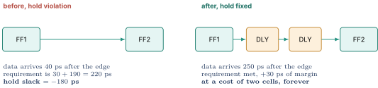
Two practical points. Hold fixing happens after CTS, because before CTS the skew is a guess and buffers inserted against a guess get removed later. And you cannot fix a 180 ps violation with exactly 180 ps of buffers, because the delay chain is itself subject to the variation of 6.4 and to its own corner spread, so you insert margin and therefore more cells than the arithmetic suggests.
7.4 The asymmetry, which is the point
| Setup fix | Hold fix | |
|---|---|---|
| What it buys | frequency, which is product performance | nothing except correctness |
| What it costs | area, power, sometimes latency | area, power, added capacitance on the path |
| When it fails | chip is slower, ship it at a lower speed grade | chip is broken at every frequency and is scrap |
| Available levers | eight, listed in 7.1 | one |
| Corner | slow | fast |
Setup fixes buy performance. Hold fixes buy nothing but correctness. That is why designers work to avoid creating hold problems rather than fixing them. Excessive useful skew creates them. Aggressive clock gating creates them, because from section 4.3 of Power Fundamentals and Clock Gating every ICG adds insertion delay on one branch, and going from 60 to 95 percent coverage adds thousands of endpoints whose clock arrives later than their neighbors. Poorly balanced clock trees create them. Every one is a decision made upstream by somebody optimizing something else.
A large block can end up with tens of thousands of hold buffers. At around 1.2 square microns and 20 nW of leakage each, 40,000 of them is roughly 48,000 square microns and about 1 mW of leakage plus switching power, spent entirely on making the design not-wrong. That is the price of the upstream decisions, and it is invisible unless somebody counts.
08.Part 8, physical design, and what your RTL does to it
8.1 The flow, end to end
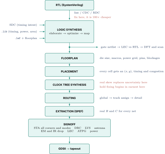
Two features are worth naming. The loop back gets more expensive left to right. A lint fix costs an hour, a synthesis-stage RTL fix costs a day, an RTL fix after routing costs weeks because everything downstream is redone and a month of placement tuning is thrown away. And CTS is the hinge. Everything before it works with estimated clock behavior and everything after it works with the real thing, so the design changes character at that moment.
8.2 Floorplanning, and why it cannot be recovered
Floorplanning decides die area and aspect ratio, places hard macros meaning SRAMs and analog blocks and IP, builds the power grid, fixes pin locations on the block boundary, and defines placement blockages and power domain regions. It is the highest-leverage and least-recoverable step, for a geometric rather than an algorithmic reason. Placement, CTS, and routing can all move cells and wires. None of them can move a 200 micron SRAM macro, and none of them can move a pin. If a macro sits between two blocks that talk constantly, every wire between them routes around it, and the extra distance is a physical fact no optimizer can argue with.
Three concrete mistakes and their signatures. Macro pins facing away from the logic that uses them, adding the macro's full width to every access path. Long thin blocks whose aspect ratio forces wires along the long dimension. Pins on the wrong edge, so a signal arriving north is consumed by logic forced south by a macro. A bad floorplan cannot be recovered later by any amount of optimization, which is why it is revised many times and why a designer who knows which of their blocks talk to each other should be in that conversation.
8.3 Placement, and why wire load models stopped working
Placement assigns coordinates to every standard cell, balancing total wirelength, timing on critical paths, congestion, and density, since the tool must leave room for buffers, delay cells, and later ECOs. The useful intuition is that placement is where wirelength stops being an estimate. Before it, synthesis uses a wire load model, a statistical guess relating fanout and block size to net capacitance. Those guesses were adequate when gate delay dominated and are badly wrong now that wire delay is comparable, which is exactly why physical synthesis in 8.7 exists.
8.4 Clock tree synthesis, and the moment the design changes character
CTS builds the physical clock network, inserting hundreds or thousands of clock buffers to deliver the edge from one source to every flop, per Clocking Reset and Domain Crossing. Its objectives are low skew between related endpoints, low insertion delay so the tree does not eat the period, tolerable clock power, and enough robustness that OCV does not wreck it.
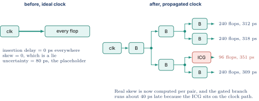
Three consequences follow from that picture. Uncertainty drops per 3.2, because skew is computed rather than reserved, and forgetting to drop it double-counts. Hold fixing begins in earnest per 7.3, because you finally know which pairs have a skew that hurts, and pre-CTS hold numbers were noise. And the clock gating cells from Power Fundamentals and Clock Gating become a physical problem here, because an ICG adds insertion delay to its branch, so CTS must either match every other branch to it, slowing the tree and adding clock power, or accept skew between gated and ungated regions, which creates hold work. Going from 60 to 95 percent gating coverage multiplies the number of such branches, and naming that cost is what makes a gating result credible.
8.5 Routing and congestion, which is where your RTL bites
Routing runs in three passes. Global routing assigns nets to coarse regions. Track assignment picks tracks within layers. Detailed routing produces actual geometry obeying spacing, via, and every other rule in the deck.
Congestion is more wires needing to cross a region than there are tracks. Make it arithmetic rather than a vibe.
  ROUTING SUPPLY vs DEMAND across one 100 um cut

  Track pitch                        0.080 um
  Tracks per layer across 100 um     100 / 0.080          = 1250
  Horizontal routing layers          4  (M2, M4, M6, M8)
  Raw supply                         4 x 1250             = 5000 tracks
  Reserved for power straps,
    clock, and blockages             -30%                 = 3500 usable

  Now put an 8-port, 64-bit full crossbar in the middle of that region.
  Every source must reach every destination, so at the widest cut:

      8 sources   x 64 bits  = 512 wires in
      8 dests     x 64 bits  = 512 wires out
      plus select and valid  ~  80 wires
                            -----------------
                              1104 wires, ALL crossing the same cut

  That fits 3500. Now make it 32 ports:
      32 x 64 x 2 + control  =  4200 wires  >  3500 available.   UNROUTABLE.
When the router cannot complete, the fix is to spread the cells out, which increases the area the structure occupies, which lengthens every wire inside it, which makes it slower. That is the cruel part. Congestion converts an area problem into a timing problem, and it does it to the exact structure you were trying to make fast.
The structures causing it are ones you write in RTL, so know them by name. Crossbars and full bypass networks from Execution Units, where wire count grows as sources times destinations times width, which is the physical reason real machines use clustered execution with limited or delayed bypass between clusters. Wide muxes and barrel shifters from Arithmetic Hardware, where every stage touches every bit, so the structure is mostly wires with a few transistors between them. High-fanout nets, where a signal driving 5,000 loads needs a buffer tree of hundreds of cells spread across the block, each occupying placement space a region wanted for something else, which is why Clocking Reset and Domain Crossing cares about reset tree design. Wide multi-ported register files and CAMs from Arbiters FIFOs and CAMs and SRAM Arrays and ECC, where every added port multiplies bitlines and wordlines and a CAM broadcasts its key to every entry.
8.6 Wire delay does not scale, and here is the arithmetic
This is the most important physical fact for a microarchitect and the one that most reliably surprises people, so derive it.
Wire resistance per unit length is for width and thickness . Shrink both by the usual per node. Cross-section falls by , so resistance per unit length rises by . Capacitance per unit length stays roughly constant, because the wire's plate capacitance to the layers above and below falls as it thins, while the spacing to its neighbors shrinks so lateral coupling rises, and the two largely cancel. So RC per unit length roughly doubles every node. Meanwhile gate delay falls by roughly per node. And crucially, wires do not get shorter just because transistors did, since a wire crossing a block is as long as the block and blocks do not shrink when you add more of them.
| Node | Gate delay (relative) | RC per mm (relative) | Wire delay per mm in gate delays |
|---|---|---|---|
| 1.00 | 1.00 | 1.0x | |
| minus one node | 0.70 | 2.04 | 2.9x |
| minus two nodes | 0.49 | 4.16 | 8.5x |
| minus three nodes | 0.34 | 8.5 | 25x |
A millimetre of wire that cost three gate delays a few generations ago costs dozens now. That is why long-wire structures became the limiter and short-logic structures did not.
Nobody accepts the raw quadratic, so the flow fights back with repeaters, and the optimization is worth working because it explains why buffer insertion is a first-class flow step. A distributed RC wire has delay proportional to . Break it into equal segments with a buffer between each and the wire portion becomes while the buffer portion becomes buffer delays. Take a 1 mm wire whose unbuffered delay is 500 ps and a buffer delay of 20 ps.
| Segments | Wire delay | Buffer delay | Total |
|---|---|---|---|
| 1 | 500 ps | 0 | 500 ps |
| 2 | 250 ps | 40 ps | 290 ps |
| 4 | 125 ps | 80 ps | 205 ps |
| 5 | 100 ps | 100 ps | 200 ps |
| 6 | 83 ps | 120 ps | 203 ps |
| 8 | 63 ps | 160 ps | 223 ps |
Minimize by setting the derivative to zero, so , giving and 200 ps total. Notice the elegant result that at the optimum the wire delay exactly equals the total buffer delay, which is a general property of this optimization.
The consequences are concrete. Long wires cannot be made free, only made linear instead of quadratic, and the repeaters cost area, power, and placement space along the whole route. Two blocks that talk a lot should be adjacent, which is clustering in Execution Units. A flat design across a large die has unavoidably long wires, so large designs are hierarchical, with tight local communication and pipelined, budgeted links between partitions. And when a wire genuinely must cross the die, the answer is a pipeline stage in the wire, which is why the interconnects in Interconnect and AMBA have registered slices whose only job is breaking a long route into two shorter ones.
8.7 Physical synthesis, and physically aware RTL
Physical synthesis merges placement into synthesis, so the optimizer places cells as it maps them and sees estimated real wirelength rather than the fanout-based statistic of 8.3. Sizing and buffering decisions are then made against real load estimates, the netlist handed to place and route arrives already placed, and the correlation between the synthesis timing report and the post-route report goes from embarrassing to usable. The cost is runtime and a heavier input set, since the tool now needs the floorplan, the physical library, and the technology file.
All of Part 8 collapses into a short list of things a designer controls before any tool runs. Keep structures that must be fast local, and accept an extra cycle for anything crossing the block. Prefer a partial or pipelined bypass network to a full one at high port count. Watch fanout on control signals and pipeline broadcasts rather than letting the tool build a 500-cell buffer tree. Think about where the SRAMs will sit, because their pins are fixed and the logic reading them must go near those pins. Structure the hierarchy so boundaries fall between blocks that do not communicate much. And know which of your paths are near-critical, because that is the information the physical designer does not have and cannot recover from the netlist.
09.Part 9, signoff and the front-end to back-end handoff
9.1 Timing signoff
Every corner and mode from 6.3, with no violations, or a written waiver per violation naming the reason and the owner. Signoff STA uses extracted parasitics rather than estimates, signoff-grade delay calculation, and the agreed OCV settings. It is run by a signoff tool deliberately different from the implementation tool, so an optimism in the implementation engine does not sign off on its own work.
A word on waivers, because that is where discipline lives. A waiver saying "this is a false path" is acceptable only if somebody can say why, and the why belongs in a reviewed document rather than a comment. A waiver list growing quietly across a project is a reliable early symptom of a schedule about to slip.
9.2 Physical verification
DRC, design rule checking, confirms the drawn geometry obeys manufacturing rules, meaning minimum widths and spacings, via enclosure, density rules requiring metal be neither too sparse nor too dense for planarization, and thousands more. A violation means the mask cannot be made or the feature will not print reliably. LVS, layout versus schematic, extracts a netlist from the geometry and compares it device by device and connection by connection to the intended netlist, catching the bug where the layout is legal and beautiful and connects the wrong things.
Antenna checks are worth explaining mechanically rather than naming. Metal layers are patterned by plasma etch, and a partially built wire connected only to a transistor gate collects charge from the plasma. The gate oxide is a few atomic layers thick and the charge has nowhere to go, so it discharges through the oxide and damages it. The larger the metal area attached to the gate before a diffusion connection exists, the more charge collects, hence the rule limiting metal-area-to-gate-area ratio per layer. Fixes are a small diode to substrate giving the charge a path, or jogging the route to a higher layer so the long segment is built after the connection exists.
9.3 Electromigration and IR drop
Electromigration is metal atoms physically migrating under momentum transfer from the electron flux, opening voids where metal thins to a break and piling up hillocks that short to a neighbor, over months or years. Mean time to failure follows Black's equation, , so it worsens with the square of current density and exponentially with temperature.
Put a number on it. Copper limits are on the order of 1 mA per micron of wire width at operating temperature, so a minimum-width 0.05 micron signal wire tolerates roughly 50 microamps. Now compute the current in a clock buffer driving 200 fF at 3 GHz and 0.9 V, where the activity factor is 1.0 by definition.
Ten times over the limit for a minimum-width wire. That is why clock nets and power rails are the EM hotspots, getting wide wires, multiple vias, and dedicated checking, while ordinary low-activity signal wires rarely have a problem. Signal EM is usually limited by RMS current and self-heating while power and ground rails are limited by average unidirectional current, and the checks differ for that reason.
IR drop is the voltage lost across the resistance of the power grid between package bump and cell. A block drawing 8 A peak through 2 milliohms from bump to far corner loses mV. Against 0.9 V that is 1.8 percent of supply, and delay sensitivity near nominal is roughly 1.5 to 2 percent of delay per 1 percent of supply, so about 3 percent of delay. On a 333 ps period that is 10 ps taken off every path in the region, and it is not in your timing report unless the flow feeds the IR map back into STA, which good flows do. Dynamic droop from through package inductance is larger and faster and is the subject of DVFS Droop and Thermal. Note also that coarse clock gating and power gating from Power Fundamentals and Clock Gating produce exactly the abrupt current steps that drive droop, so a power optimization is also a power integrity risk.
9.4 Equivalence checking
Logic equivalence checking proves the gate netlist implements the same function as the RTL, formally and exhaustively, without simulation. The tool matches key points, meaning primary inputs, primary outputs, and register outputs, then proves the combinational cone feeding each matched point is identical on both sides. It is fast because the problem decomposes at every register and complete because it is a proof rather than a sample. See Verification Methodology.
What matters here is what breaks it, because each break has a flow answer. Retiming moves registers so key points no longer correspond, requiring sequential equivalence checking, which is far more expensive and sometimes inconclusive. Clock gating insertion changes the netlist structurally, so the tool must be told to treat the gated clock as equivalent to the ungated one under the enable. Scan insertion adds a mux at every flop's data input, so the comparison runs with scan tied off. ECOs applied directly to the netlist late in the flow are the changes most likely to be wrong and least likely to be re-verified, which is why LEC re-runs after every one.
9.5 DFT coverage and the front-end static checks
Stuck-at and transition fault coverage from ATPG per DFT and Silicon Debug, typically targeting the high nineties. DFT is not a separate universe. Scan chains add a mux delay to every flop's data path and add routing. Test modes are additional modes in the MCMM matrix of 6.3. Clock gating cells need their test enables wired up or whole chains go untestable. And at-speed transition testing needs the capture path to meet functional timing, making it a genuine timing mode rather than a formality.
The front-end static checks run on RTL long before any of that. Lint checks style and structural hazards against a rule deck, catching inferred latches, incomplete sensitivity lists, width mismatches, multiply driven signals, and a long list of patterns that are legal Verilog and bad hardware, per RTL Design and SystemVerilog. CDC checking structurally verifies every clock domain crossing, confirming a synchronizer exists, that it is the right kind, that multi-bit crossings use gray coding or a handshake rather than independent synchronizers, and that no combinational logic sits between source flop and synchronizer where it could glitch, per Clocking Reset and Domain Crossing. This is the check that makes the false paths of 4.2 safe. RDC does the same for reset domain crossings, where a flop reset by one reset feeds a flop reset by another, so de-asserting one while the other is active can capture an unstable value.
The economic argument for all three is simple. An RTL bug caught by lint costs an hour, the same bug at signoff costs weeks, the same bug in silicon costs a respin. The static checks are the cheapest quality per dollar anywhere in the flow, which is why upgrading a lint and physical verification flow across a group is worth more than it sounds.
9.6 The handoff itself
What changes hands between front end and back end, at least once and usually many times, is worth knowing because it is what the meeting is about. Going forward it is the frozen RTL with a change log, the SDC including the exception list with justifications, the floorplan constraints and pin assignment negotiated rather than dictated, the input and output delay budget agreed with neighboring block owners per 3.3, the list of near-critical paths and the structures the designer knows are risky, the power intent file per Part 8 of Power Fundamentals and Clock Gating, and the DFT requirements, chain count, and test modes. Coming back the other way it is timing reports, congestion maps, IR maps, and the list of things that will not close without an RTL change.
That last item is the interesting one, because it is where physical reality comes back and asks the designer to change the microarchitecture. Handling it well is a large part of what makes an RTL engineer valuable rather than merely competent.
10.Part 11, check yourself
Answer out loud, in full sentences, as if an interviewer asked. If you cannot, reread the section named.
- Why is an AND gate's delay not a single number, and what two things is it a function of? Sketch how the tool gets a delay for a point not in the table. (1.2)
- State the governing principle of synthesis in one sentence, then give one concrete example of an unconstrained path being left slow and one of a wrongly constrained path being over-optimized. (1.3, 2.2, 2.4)
- Walk the three phases of synthesis and say what each produces. Where does resource sharing happen, and why is it a tradeoff rather than a win? (2.1, 2.2)
- What do
set_input_delayandset_output_delaydescribe? Work the budget for a 1 ns block with 300 ps of input delay, then explain exactly how a block closes standalone and fails at integration. (3.3) - What is
set_clock_uncertaintyreserving margin for, and what must change about it after clock tree synthesis? What happens if you forget? (3.2, 8.4) - Give two concrete false paths and say what makes each genuinely false rather than merely hard. Why is
set_clock_groups -asynchronoussafer than hand-written false paths? (4.2) - Declare a two-cycle setup multicycle on a 500 ps clock and work out exactly what happens to the hold check. What is the fix, and what design-level claim are you making by declaring it at all? (4.3)
- Explain why a missing exception and a wrong exception are dangerous in different ways, and which you would rather have. (4.5)
- Define arrival, required, and slack, and compute all three given the clock network delays, cell delays, uncertainty, and setup time. Where does skew appear in that arithmetic? (5.3)
- WNS is -40 ps and TNS is -95 nanoseconds across 3,200 endpoints. What shape is the histogram and what would you do? Now WNS is -210 ps and TNS is -210 ps. Same questions. (5.5)
- Which PVT corner is worst for setup and which for hold, and why in each case? Then explain temperature inversion and why it means you cannot just check the hot corner. (6.1, 6.2)
- Derive why a 20-stage path should be derated less than a 2-stage path. What is common path pessimism removal, and how many picoseconds does it recover on a path with 280 ps of shared clock tree at a 5 percent derate? (6.4)
- List the setup levers in order of preference and justify the order. Then explain why hold has exactly one lever and why hold fixes cost money and buy nothing. (7.1, 7.3, 7.4)
- Name four RTL structures that cause routing congestion, say what happens physically when the router cannot complete, and derive why wire delay does not scale with process the way gate delay does. (8.5, 8.6)
- Name the signoff checks and say what each proves that the others do not. Explain the antenna effect mechanically rather than by name. (9.1 to 9.5)
11.Part 12, related notes
- Digital Logic and Timing for the setup and hold equations, skew and jitter, and where gate delay comes from, which is what everything here rests on
- RTL Design and SystemVerilog for what synthesis reads, inferred latches, and lint-clean coding practice
- Power Fundamentals and Clock Gating for the ICG insertion delay behind the CTS and hold cost of high gating coverage, for multi-Vt swapping, and for the UPF the flow also consumes
- DVFS Droop and Thermal for the operating points that become corners in the MCMM matrix, and for droop beyond static IR drop
- Clocking Reset and Domain Crossing for clock tree synthesis, why a CDC path is a legitimate false path, and CDC and RDC checking
- Verification Methodology for equivalence checking, gate-level simulation, and the formal reasoning that should back an exception rather than an assertion in a file
- DFT and Silicon Debug for scan insertion, ATPG coverage, and why test modes multiply the MCMM matrix
- Execution Units for bypass networks and clustering, the microarchitectural consequence of 8.6
- Arithmetic Hardware for the adder and multiplier structures the tool chooses between during technology mapping
- Interconnect and AMBA for registered slices, which are pipeline stages existing only to break long wires
- From Logic to Silicon for the vault's treatment of transistors, standard cells, and PPA concepts
- Trends, Constraints, and Quantitative Principles for the vault's treatment of scaling and the trends behind Part 8