SoC Integration and Interfaces
September 8, 202665 min readadvanced
Block A is a DMA engine. It passes 100 percent of its assertions and its coverage closed weeks ago. Block B is a memory controller, same story. Both are correct. Wire A's AXI master to B's slave through the…
01.Part 1, what integration actually is
1.1 Two blocks that both work, and a chip that does not
Block A is a DMA engine. It passes 100 percent of its assertions and its coverage closed weeks ago. Block B is a memory controller, same story. Both are correct. Wire A's AXI master to B's slave through the fabric, boot the chip, and it hangs on the first transfer.
Nothing in either block is broken. Block A's designer assumed that once reset de-asserts the fabric is alive and will answer immediately. Block B's designer assumed the mirror image, that nobody sends traffic until his 64-cycle DRAM initialization finishes and init_done goes high. Neither assumption is written anywhere and neither is wrong in isolation. A was tested against a fabric model that answered instantly. B was tested against a stimulus generator that politely waited for init_done, because the person who wrote it also wrote the controller.
At integration A issues a read three cycles after reset release. B is on cycle 3 of its init and does not accept it. The fabric holds the transaction, A waits forever for a response, B finishes init and sits idle because nothing re-issues. Deadlock, no assertion fires, and the waveform shows two blocks each behaving exactly as designed.
That is integration. It is not wiring. It is the discovery of every unwritten assumption at the moment two designs meet.
1.2 Where the schedule risk actually comes from
Count the surface, because the intuition that integration is just connecting things survives only until you do. Take 40 top-level blocks. For each, the integrator must get right its clocks, resets, power domain, interfaces, address ranges, interrupts, test hookup, and boundary timing. Eight categories, each holding roughly four facts, since "clocks" means which clocks, at what frequency, in what phase relationship, and which crossings are asynchronous. That is facts. Suppose each is independently right with probability 0.995, optimistic for information passed between teams by email and hallway conversation. Expected wrong facts is , so six or seven silent errors in a design where everything looks connected.
The count is half the problem. The other half is when they surface.
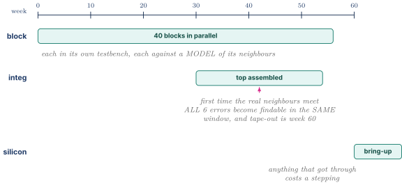
Three effects compound there. The bugs cannot be found earlier, because until the real neighbour exists you test against a model encoding the same assumption the designer already made. Full-chip simulation is one to three orders of magnitude slower than block simulation, so a twenty-minute debug loop becomes a day. And every bug is cross-team, so debugging one needs two or three designers who each believe the problem is in the other block. Cheap to make, expensive to find, all arriving at once where the schedule has least slack.
1.3 The two kinds of integration bug
Structural bugs are wrong wires. Something unconnected, a bus joined at the wrong width so the top bits truncate silently, an active-low reset on an active-high port, swapped byte lanes, a clock from the wrong PLL output. All statically detectable. Lint catches width mismatches and floating inputs, connectivity checks catch missing connections, formal equivalence catches RTL-to-netlist divergence, CDC and RDC tools catch missing synchronizers. In a well-run flow this class is close to fully automatable, and every escape is a flow failure rather than a design failure. That is exactly what a group-wide lint and physical-verification flow upgrade buys.
Behavioral bugs are correct wires carrying a legal but wrong sequence. The 1.1 deadlock is one. So is a reset released out of order, an interrupt that fires before its handler's block is enumerated, a domain woken without waiting for its rail acknowledge, an address decoded to two blocks so both respond, a DMA descriptor read before the software store to it was ordered. No static tool sees any of these, because every wire is right.
So static checking proves the connections are right and directed sequencing tests prove the ordering is right, the same pairing as static power-intent checking against power-aware simulation in section 8.3 of Power Fundamentals and Clock Gating. Neither finds the other's bugs, and a plan that funds one will find the second class in silicon.
02.Part 2, the anatomy of an SoC
2.1 The map
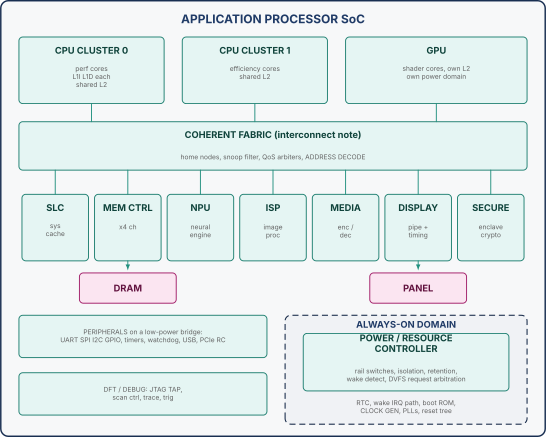
Keep that in mind for Part 10, because it means you have already lived on one edge of this diagram rather than looking at it from outside.
2.2 The blocks want incompatible things
Integration is not "attach everything to a bus," because these blocks have almost nothing in common as fabric clients. A display pipeline feeding a 3840 by 2160 panel at 120 Hz with 4 bytes per pixel must fetch MB per frame, so GB/s, continuously. That is not an average it can make up later. If the pixel FIFO underruns for one microsecond the panel shows a visible tear. The display does not care about latency at all, since its FIFO is hundreds of lines deep, but it has a hard deadline on aggregate delivery.
A CPU load missing to DRAM wants the opposite, trivial bandwidth but every nanosecond of latency lost directly to a stall. The GPU and NPU want raw throughput and tolerate latency happily. The ISP and media decoders want a deadline per frame. Peripherals want nothing but correctness. Every one of those is a different power domain, most are different clock domains, and they all contend for the same DRAM. Reconciling them is the QoS discussion of Part 5 of Interconnect and AMBA, and it is an integration decision because no single block author can see the conflict.
2.3 Where blocks come from
| Source | Arrives as | You can change | Main risk |
|---|---|---|---|
| Internally designed | RTL you own | anything | your own assumptions, per 1.1 |
| Licensed soft IP | RTL, often encrypted, plus an integration guide | configuration parameters only | the guide is a document, and documents are wrong |
| Hard macro | GDSII layout, a LEF abstract, a Liberty model | nothing at all | it lands on your floorplan first |
Soft IP synthesizes into your flow, so you pick the library, the frequency, the placement. What you lose is visibility, since encrypted RTL means that when it misbehaves you file a support ticket and wait weeks. The realistic mitigation is to wrap it, assert on every one of its interfaces yourself, and never send a bug report without a waveform proving the violation is on their side.
Hard macros reshape your job. SRAM compiler output, PLLs, SerDes PHYs, analog front ends, eFuses. They arrive as finished layout, so their width, height, pin positions, and internal routing blockages are facts about your chip before you have written the logic around them.
2.4 Hard macros own the floorplan before you place a cell
Standard-cell placement is an optimization over a remaining area. The placer takes what is left after macros, keepout halos, and blockages are subtracted, so macro placement is not one step among many, it defines the domain of every step after it.
Work a partition. You own 3 mm by 3 mm, so 9 mm². In it go six SRAM macros at 1.20 by 0.90 mm and a PLL at 0.50 by 0.50 mm, which is mm², so 75 percent gone before a gate exists. Add a 20 µm keepout halo around each, because the placer cannot legally place cells against a macro edge and the router needs a channel, and the haloed total is about 7.28 mm². Remaining cell area is 1.72 mm², and at a realistic 65 percent placement utilization the usable cell area is mm². If your netlist needs 1.5 mm² the block does not fit, and no placement effort fixes it. Fewer SRAMs, a bigger partition taken from a neighbour, or a microarchitecture change. That decision is made at floorplan time, months before the logic is finished, on an area estimate, which makes a wrong estimate one of the most expensive integration errors available.
The second constraint is pin location.
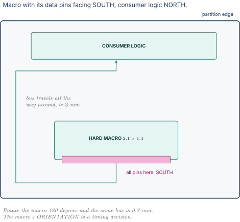
An optimally buffered global wire runs on the order of 100 ps per millimetre, an order-of-magnitude figure varying from roughly 50 to 200 with metal layer and repeater strategy. At 100 ps/mm the 3 mm detour costs 300 ps. At 3 GHz the period is 333 ps. The detour caused by macro orientation consumed the entire cycle, and no synthesis effort recovers it because the wire is the path. That is why hard macros constrain the floorplan before standard-cell placement. Not a tool-ordering convention, but because macros fix both the available area and the wire lengths, and those two together decide whether the block can be built.
03.Part 3, the integration contract
Part 1 says the failures come from unwritten assumptions, so the fix is to write them down per block in a checkable form. Producing this checklist from memory is the clearest signal that you have integrated a block rather than only designed one, because a block designer has no reason to hold all eight categories at once.
3.1 The checklist
 +=====================================================================+
 |           INTEGRATION CONTRACT for block <NAME>       rev ___       |
 +=====================================================================+
 | [ ] 1 CLOCKS     source PLL, frequency, duty, jitter budget         |
 |                  phase relationship to every clock it touches       |
 |                  ASYNC crossings -> synchronizer + CDC signoff      |
 |                  RATIO-SYNC crossings -> enable scheme, no sync     |
 |                  which clocks may be stopped, and by whom           |
 | [ ] 2 RESETS     domains, async assert / sync release per domain    |
 |                  RELEASE ORDER vs every neighbour, and why          |
 |                  reset domain crossings -> RDC signoff              |
 |                  what state survives reset, what does not           |
 | [ ] 3 POWER      domain membership, always-on portion if any        |
 |                  retention set, save/restore control source         |
 |                  isolation, which outputs, CLAMP VALUE per signal   |
 |                  wake sequence and WAKE LATENCY budget              |
 |                  quiesce protocol, how it proves it is idle         |
 | [ ] 4 INTERFACES protocol and revision, data width, ID width        |
 |                  OUTSTANDING transactions issued / accepted         |
 |                  ordering guarantees REQUIRED and PROVIDED          |
 |                  QoS class, bandwidth need, latency tolerance       |
 |                  error response, SLVERR / DECERR handling           |
 | [ ] 5 ADDR MAP   ranges it RESPONDS to, size, alignment, paging     |
 |                  ranges it MASTERS onto, its ID / stream ID         |
 |                  security attribute per range                       |
 | [ ] 6 INTERRUPTS which, level or edge, active polarity              |
 |                  target controller, input number, priority          |
 |                  how cleared, and whether it can WAKE a domain      |
 | [ ] 7 TEST       scan chain count and length, stitch order          |
 |                  own MBIST / LBIST, controller, run time            |
 |                  JTAG access, what is forced during shift           |
 | [ ] 8 TIMING     input/output delay budget IN PICOSECONDS           |
 |                  who owns the wire between the blocks               |
 |                  max transition and max cap at the boundary         |
 |                  false and multicycle paths, with justification     |
 +=====================================================================+
3.2 Clocks and resets
The clock question is not just frequency, it is what relationship each pair has, because that decides whether a crossing needs a synchronizer, an enable scheme, or nothing. Synchronous means same frequency and edge from the same source, timed normally. Ratio-synchronous means integer-related and phase-aligned, for example 2.4 GHz and 800 MHz from one PLL by divide-by-3, so every third fast edge coincides and a path can be timed statically given a pulse enable marking that cycle. Mesochronous means same frequency, unknown fixed phase. Asynchronous means unrelated sources, the only case needing a synchronizer and full CDC signoff per Clocking Reset and Domain Crossing.
| Crossing | Source | Destination | Relationship | Treatment |
|---|---|---|---|---|
| core to L2 | 2.4 GHz PLL0 | 2.4 GHz PLL0 | synchronous | normal STA |
| L2 to fabric | 2.4 GHz PLL0 | 800 MHz, PLL0 3 | ratio-synchronous | enable-gated path, static timing |
| fabric to DRAM ctrl | 800 MHz PLL0 | 933 MHz PLL1 | asynchronous | async FIFO, gray pointers, CDC signoff |
| fabric to peripherals | 800 MHz PLL0 | 100 MHz PLL0 8 | ratio-synchronous | enable scheme |
| any to always-on | any | 32 kHz RTC | asynchronous | two-flop sync, control only |
The cheap mistake is treating a ratio-synchronous crossing as asynchronous. It works, and it costs two cycles of latency plus an unnecessary FIFO on the path carrying all memory traffic. The expensive mistake is the reverse, calling a crossing ratio-synchronous because two PLLs "are both set to 800 MHz." Two PLLs at the same nominal frequency are still asynchronous, since their phase is unconstrained and drifts. That crossing passes simulation, passes STA, and fails on some fraction of parts at some temperature.
Resets need the domain, whether reset is asynchronously asserted and synchronously released, and where the block sits in the release order. State the ordering as a dependency rather than a list. A block must be out of reset before anything that can send it a transaction, which makes the order a topological sort of the talks-to graph, from slaves toward masters. So the always-on controller comes up first, then clock generation and PLL lock, then the fabric, then memory controller and system cache and peripherals, and the CPU cluster comes last, because a core fetches the instant it is released and that fetch must find a working path all the way to DRAM. Skipping a step fails silently. Release the fabric after the memory controller and the controller's first refresh command is dropped, so DRAM loses content. Release the CPU before the system cache and the first fetch gets no response, so the core hangs at the reset vector with no error anywhere.
The related item is reset domain crossing. When domain A resets and B does not, A's outputs change asynchronously with respect to B's clock, structurally the same hazard as a clock crossing and needing its own signoff tool, since the CDC tool will not find it. It prevents a control FSM in B taking a transition off a glitch caused by A's reset assertion, landing B in a state its designer proved unreachable.
3.3 Power
From Power Fundamentals and Clock Gating, five entries. Which domain and whether any part must be always-on. Which registers retain and what drives save and restore. Which outputs need isolation and, critically, what value each clamps to, since a request clamping to 1 makes a sleeping block appear to demand service forever. What the wake sequence is. And how the block proves it is quiescent so the controller may safely remove power.
The number no block designer will produce for you is the wake latency budget, which software needs for the break-even arithmetic of 6.3 of Power Fundamentals and Clock Gating.
| Step | Time | Why |
|---|---|---|
| wake request reaches controller | 0.1 µs | synchronizer plus controller cycles |
| staged rail ramp, daisy chain | 6.0 µs | deliberately slow to bound |
| rail-good confirmed by chain ack | 0.5 µs | detection plus margin |
| PLL relock, if the PLL was off | 4.0 µs | loop settling |
| retention restore, reset release, ungate, isolation release | 0.28 µs | all trivial |
| un-quiesce, allow traffic | 0.1 µs | fabric handshake |
| total | µs |
Read the shape, not the total. Rail ramp and PLL relock are 10 of the 11 µs and everything else is noise. That says where a wake-latency effort goes, and it tells software that keeping the PLL alive through sleep buys back 4 µs at the cost of the PLL's own power. Stating the trade in that form is what "power contract" means.
3.4 Interfaces, interrupts, and test
Protocol, width, outstanding capability, ordering, QoS class. The one that gets missed is outstanding capability. A block on a 128-bit AXI at 800 MHz has a peak of GB/s. Round-trip latency to DRAM at its boundary is 120 ns and transactions are 64-byte lines, so by Little's law from 7.1 of Interconnect and AMBA the number in flight is arrival rate times latency.
It needs 24 outstanding to keep its own interface busy. If the designer implemented 8, achievable bandwidth is percent, or 4.3 GB/s, and no fabric tuning changes that. This belongs in the contract because it is invisible from either side alone. The block designer sized against a testbench latency of 30 ns and got 8 right for that, and the integrator knows the real number is 120 ns. Neither knows the other's until somebody writes both down.
For interrupts, record which condition raises each one, level or edge and polarity, which controller input and priority, how software clears it, and whether it is on the wake path. That last entry is the one that bites. A level interrupt that can wake a power-gated cluster must stay asserted through the entire 11 µs sequence of 3.3, because if it drops partway the cluster wakes, finds nothing to service, and sleeps again with the event lost. An edge interrupt on a wake path is worse, since the edge arrives while the receiving controller may be gated. Anything on the wake path must be captured in an always-on latch, and that latch is what the controller polls.
Test details are in DFT and Silicon Debug. The integration-specific item is that scan chains are stitched across block boundaries at the top, so a block delivering three chains of 4000 flops where the plan assumed six of 2000 doubles shift time for every pattern on the whole chip. Shift time multiplies by pattern count, which makes it a direct tester-cost item, and tester cost is per part.
3.5 The timing budget at the boundary
Two blocks are synthesized and placed separately, and a path from a flop in A to a flop in B is seen whole by neither tool. So the period is divided in advance by agreement, and each side is constrained to its share. Work it at 800 MHz, a 1250 ps period.
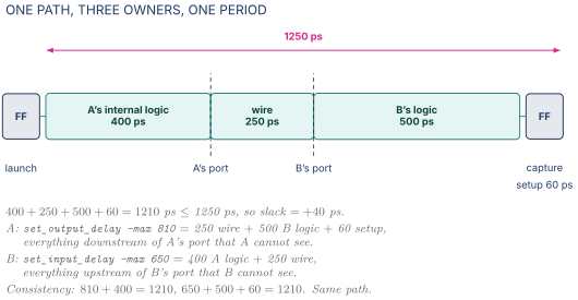
Now the failure this prevents. Nobody writes the budget down, and each team assumes "we get most of the cycle, the other side is a thin wrapper." A constrains to 60 percent with set_output_delay 500, leaving itself 750 ps. B does the same with set_input_delay 500, leaving itself 690 ps after setup. Both close timing, both sign off, and the real path is ps against a 1250 ps period. 500 ps over, and neither report shows it because neither tool saw the whole path. It appears for the first time at top-level closure, when both blocks are placed, routed, and frozen, and the fix is repipelining one of them. The budget must be allocated centrally and the sum must be checked, in picoseconds rather than percentages, because 60 percent of a period is a different number the moment somebody moves the frequency target.
04.Part 4, address maps
4.1 A map, concretely
On a 40-bit physical address, so TiB of space.
| Range | Size | Owner | Attributes |
|---|---|---|---|
0x00_0000_0000 to 0x00_0000_FFFF | 64 KiB | boot ROM | read only, secure |
0x00_1000_0000 to 0x00_1000_3FFF | 16 KiB | UART0 | device, non-secure |
0x00_1000_4000 to 0x00_1000_7FFF | 16 KiB | UART1 | device, non-secure |
0x00_1004_0000 to 0x00_1007_FFFF | 256 KiB | DMA engine registers | device, non-secure |
0x00_2000_0000 to 0x00_2FFF_FFFF | 256 MiB | GPU registers and aperture | device, non-secure |
0x00_3000_0000 to 0x00_300F_FFFF | 1 MiB | secure enclave | device, secure only |
0x01_0000_0000 to 0x02_FFFF_FFFF | 8 GiB | DRAM | normal, cacheable |
| everything else | unmapped | must return an error |
Three properties are load-bearing and none are obvious. Every range is a power of two and aligned to its own size. Every independently assignable device gets at least one full page. DRAM is one contiguous run with no holes in it. The next three sections say why each is true.
4.2 Decode depth
Somewhere in the fabric, combinational logic looks at an address and picks one of, say, 64 targets. It sits in the request path, so its delay is added to every transaction in the system.
Take the aligned case. UART0 owns 0x00_1000_0000 for 64 KiB. Since 64 KiB is and the base is 64 KiB aligned, the low 16 bits are don't-care and membership is exactly "the top 24 bits equal 0x001000." That is 24 XNORs feeding an AND tree, and an AND tree over 24 inputs with 2-input gates is levels, so 6 gate delays, or 120 ps at 20 ps per level.
Now the unaligned case. Specify the same UART as base 0x00_1000_3000, length 50000 bytes. Neither aligned nor a power of two, so membership needs and , two 40-bit magnitude comparisons. A magnitude comparison is not an equality test, it is a carry-like computation where bit 's result depends on every bit above it, so a tree implementation is roughly levels of larger cells, call it 15 gate delays, or 300 ps.
Then multiply by fan-in. With 64 targets you run 64 comparisons in parallel, get a one-hot, and encode it in another levels. Aligned totals 12 levels, so 240 ps, which against 1250 ps is 19 percent of the fabric cycle spent deciding who the request belongs to before any transport happens. Unaligned would be 21 levels, so 420 ps, a third of the cycle. That is why the address map is a microarchitecture document rather than a spreadsheet. Align every region to its own size and make every size a power of two and the decoder is a bit-match.
4.3 Page granularity, large pages, and what software inherits
The second constraint is a security property. The IOMMU translates and checks device addresses exactly as the MMU does for software, and like the MMU its smallest unit of permission is one page. On ARM64, and on Apple silicon specifically, 16 KiB is a common base page size, with 4 KiB the other widespread choice. Take 4 KiB for arithmetic.
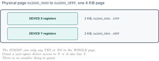
That is a real privilege escalation. If Y is a DMA engine, a driver given only X can program Y to read arbitrary physical memory. It cannot be fixed in software, in the IOMMU, or in the driver, only in the address map, which means in the chip. So the rule is a hardware rule. Any resource that might ever be assigned independently gets its own page, at the largest base page size the system supports. A device with 32 bytes of registers still consumes 16 KiB, which looks wasteful until you notice you are spending out of , one part in 64 million. Address space is free, the security hole is not. The subtler case is a device with 32 queues where each should go to a different virtual machine, since each doorbell then needs a separate page, so 512 KiB at 16 KiB pages. That is what makes SR-IOV-style sharing possible, it is decided at design time, and getting it wrong means the device can never be shared.
The third constraint comes from the TLB, which holds a fixed number of translations, per TLBs and Address Translation. Call it 512. TLB reach is entries times page size, so 2 MiB on 4 KiB pages, 8 MiB on 16 KiB pages, 1 GiB on 2 MiB pages, and 512 GiB on 1 GiB pages. A 4 GiB working set on 4 KiB pages misses constantly, since 2 MiB of reach against 4 GiB means essentially every new region walks the page table, while on 1 GiB pages the same footprint needs four entries and never misses. The difference is routinely tens of percent, which is why operating systems work hard to use large pages.
A 1 GiB page must map a naturally aligned, physically contiguous 1 GiB region. So drop a 1 MiB MMIO aperture at 0x1_4000_0000, in the middle of an 8 GiB DRAM range, and the 1 GiB-aligned region containing it now has a non-DRAM hole. The OS falls back to 2 MiB pages for that whole gigabyte, which is 512 entries, the entire TLB, to cover one gigabyte that should have cost one entry. The integrator saw a small hole in a large space. Software sees a permanent performance cliff it cannot work around. Keep DRAM one contiguous run and put every device aperture in a separate bounded region, which is the shape of the table in 4.1.
4.4 Security partitioning, holes, and the unmapped access
Modern SoCs have at least two worlds, secure and non-secure, and the structural point is that the security attribute is part of the address rather than a filter applied after decode. The decoder's input is the address plus the security bit, which means the same numeric address may legitimately decode to different targets in different worlds, and, more importantly, a non-secure access to a secure-only range is rejected at the decoder rather than at the target. Rejecting at the target makes every target part of the security boundary, so forty pieces of logic must be trusted instead of one. The failure when it is done wrong is a target that returns an error but has already had a side effect, clearing an interrupt or popping a FIFO, so the transaction "failed" and the attacker still changed state. That is why the check belongs upstream of the target's write enable.
Three defects live in the gaps of a map. Unmapped addresses must be claimed by a default slave returning a decode error, DECERR in AXI terms, immediately. The wrong behavior is a zero one-hot, so the transaction goes nowhere and the master waits forever, which from Part 4 of Interconnect and AMBA is the hardest class of bug there is because there is nothing to look at. Every SoC needs a default slave and forgetting it is a classic integration bug. Overlapping ranges produce a two-hot decode, so two targets respond and two responses arrive for one request, corrupting the fabric's transaction tracking. That is statically checkable from the map itself and should be a script in continuous integration rather than a review item. Unintended aliases happen when a target decodes fewer address bits than its range implies, so a block with 4 KiB of registers decoding only 10 bits also responds at offset 0x400, and software that writes the alias corrupts a register it never meant to touch in a way that is nearly impossible to attribute.
05.Part 5, register maps and generating them from one source
5.1 Five copies of the same fact
A block has a control register whose bit 5 is DMA_ENABLE. That single fact must be simultaneously true in the RTL decoder and flop, the C header firmware includes, the UVM register model verification predicts against, the programming guide the driver author reads, and the checklist post-silicon bring-up runs. Five artifacts, written by hand, by four different people. A medium block has 200 registers averaging 8 fields, so 1600 fields across 5 artifacts, so 8000 facts that must agree, changing dozens of times over a project. Divergence is not a risk, it is a certainty.
The failure in its commonest form. Late in the project a field moves from bit 5 to bit 6 to make room for a wider neighbour. The RTL is updated, the C header is not, because it lives in another repository owned by another team. Firmware writes bit 5, which is now RESERVED, so the enable never asserts and the block does nothing. No error appears, because writing a reserved bit is legal and reads back consistent. Three engineers spend two days on it, and that repeats every time a field moves.
5.2 One source, five outputs
Discipline fails at 8000 facts. The fix is to make four of the five artifacts derived, so they cannot diverge because they are not separately authored. Write the register once in a machine-readable language. IP-XACT is the IEEE standard, SystemRDL is the one most people prefer, and every large company has an internal equivalent. The syntax below is SystemRDL-flavoured and the point is the content rather than the keywords.
| reg ctrl { | |
| field { | |
| sw = rw; hw = r; reset = 0; | |
| desc = "Enable the DMA engine. Must be 0 while reconfiguring."; | |
| } dma_enable[5:5]; | |
| field { | |
| sw = rw1c; hw = w; reset = 0; | |
| desc = "Set by hardware on a completion error. Write 1 to clear."; | |
| } err_sticky[0:0]; | |
| }; |
| Generated output | What it is | Who consumes it |
|---|---|---|
| SystemVerilog | decoder, flops, read mux, access-type behaviour | synthesis, and it is the actual hardware |
| C header | field offsets and masks | firmware and driver authors |
| UVM RAL model | register model with predicted values and access tests | verification, per Verification Methodology |
| Documentation | tables with descriptions and reset values | everyone |
| Test collateral | generated reset-value and walking read-write tests | block sim and post-silicon bring-up |
The bit-5-to-bit-6 change now touches one line in one file and all five move together. The divergence bug class does not become rarer, it becomes structurally impossible, which is a different and better thing. The secondary benefit is uniformity, since every block's registers behave identically for the same declared access type, so a driver author who learns one has learned all of them.
5.3 Access types, where the subtlety lives
| Type | Software write | Software read | Typical use |
|---|---|---|---|
| RW | sets the value | returns the value | a configuration bit |
| RO | ignored | returns hardware value | status or ID |
| RW1C | writing 1 clears, 0 does nothing | returns the value | interrupt status |
| RW1S | writing 1 sets | returns the value | a doorbell |
| RC | ignored | returns value and clears it | a counter drained by reading |
| W1P | writing 1 emits a one-cycle pulse | returns 0 | a "start" command |
| RSVD | ignored | returns 0 | future expansion |
The RW1C race is the one that gets asked. Hardware sets an interrupt status bit when an event occurs, software clears it by writing 1. What if hardware sets in the exact cycle software's clear lands? Only two resolutions exist and they are not equally correct. If the clear wins, the bit ends 0 and the new event is lost forever, since the interrupt line drops and the handler has already finished. If the set wins, the bit ends 1, the interrupt fires again, and the handler runs once more against an event it has partly seen. Set must win. Losing an event is a hang, a spurious extra interrupt is a wasted microsecond. A generator that gets it backwards produces a device that occasionally stops delivering interrupts under load, which is among the worst bugs there is because it is rate-dependent and vanishes when you instrument it.
Read-to-clear is convenient for counters and dangerous elsewhere, because reading has a side effect. A debugger displaying the register clears it, and two threads that both read lose one increment. RC is right for a saturating performance counter drained once per interval and wrong for anything a human might look at. Two further generator responsibilities are easy to skip and expensive to skip. Byte enables must be honored, since software writing one byte of a 4-byte register must not disturb the other three, and a generator ignoring WSTRB produces registers that corrupt themselves under any driver using byte stores. Reserved bits must read zero and ignore writes, because software written against an older revision writes zeros there and breaks when the bit becomes meaningful.
5.4 Reading a 64-bit counter over a 32-bit bus
This is the register-map problem worth walking through unprompted, because it is genuine hardware-software co-design. A free-running 64-bit counter, a 32-bit bus, so software reads low then high. With the obvious implementation, where each read returns the current value of its half, watch a rollover.
| Time | Event | Counter | Software has |
|---|---|---|---|
| reads LOW | 0x0000_0001_FFFF_FFFF | low = 0xFFFF_FFFF | |
| counter increments, low rolls | 0x0000_0002_0000_0000 | ||
| reads HIGH | 0x0000_0002_0000_0000 | high = 0x0000_0002 |
Software assembles 0x0000_0002_FFFF_FFFF, a timestamp 4.3 billion counts in the future that the counter never held. Code computing a duration by subtracting two such reads now believes a one-microsecond operation took an hour, and loops built on that arithmetic hang. It happens only when a read straddles a rollover, so often enough to matter and rare enough to survive every test you write.
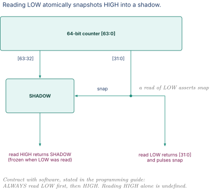
Redo the trace. At the low read returns 0xFFFF_FFFF and latches 0x0000_0001 into the shadow. The counter rolls at . At the high read returns the shadow, so the assembled value is exactly what the counter held at . Atomic, and it cost one register.
The integration-specific part is the last line of that diagram. The ordering requirement is a contract with software, invisible in the RTL, and if it is not in the programming guide the first driver author reads high first and the mechanism silently does nothing. Hardware mechanisms that depend on software following a sequence must have that sequence written down, which is the argument of Part 9.
Register implementation in the Resource Controller IP is this work. The way to raise it is not "I implemented registers," which sounds like a task, but to pick one of these hazards and say how the design handled it. The RW1C race and the shadow latch are both small, specific, and unmistakably things a person who has built register interfaces knows and a person who has read about them does not.
06.Part 6, the hardware and software interface
An ASIC design role says "collaborate with hardware and software teams." That bullet exists because hardware engineers routinely design blocks that are correct and unusable.
6.1 The programming model is a state machine
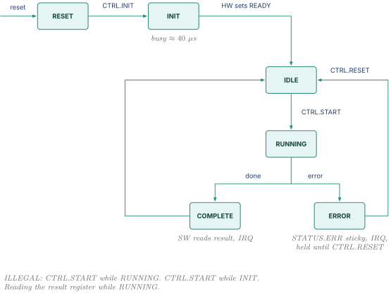
The essential decision is what an illegal action does, and there are three options. Ignore it, so the write is dropped and the block holds its state, which is safe and simple and makes software's bug silent, so a driver that starts twice appears to work until the day the timing shifts. Reject it, returning a bus error or setting a sticky error bit and raising an interrupt, so software learns at the exact instruction that did it. That is almost always right. Undefined, so the block does whatever falls out of the gates. Never acceptable, and yet it is the default whenever nobody specifies the behavior, because unspecified means the RTL does whatever the case default happened to be.
6.2 Interrupts against polling, with the arithmetic
An interrupt costs an exception entry, a context save, a controller read to identify the source, the handler, an acknowledge, a return, and on an out-of-order core a pipeline flush and a cold instruction cache for the handler. Call it 2 µs fully loaded. A device generating 500,000 events per second with one interrupt each costs second of CPU time per second, an entire core doing nothing but interrupt entry and exit. That is an interrupt storm, and the system spends all its time servicing the device and none doing the work the device exists to enable, exactly when demand is highest.
The fix is coalescing. Hold the interrupt until either events accumulate or elapses since the first uncovered event, then let software service the whole batch in one handler entry. Take and and see which threshold binds.
| Event rate | Time for 32 events | Which fires | Interrupts/s | CPU at 2 µs each | Worst added latency |
|---|---|---|---|---|---|
| 100 k/s | 320 µs | timer | 20,000 | 4.0 percent | 50 µs |
| 500 k/s | 64 µs | timer | 20,000 | 4.0 percent | 50 µs |
| 1 M/s | 32 µs | count | 31,250 | 6.3 percent | 32 µs |
| 5 M/s | 6.4 µs | count | 156,250 | 31 percent | 6.4 µs |
The timer caps the interrupt rate at no matter how fast events arrive, which is what prevents the storm. The count threshold binds only once arrivals are fast enough that 32 fit inside , and when it binds it also cuts latency, because a batch fills quickly. So the mechanism self-adjusts, costing latency when the system is idle, the one time you do not care, and almost nothing when it is busy. At 500 k/s the device delivers 25 events per interrupt, so the per-event cost is 80 ns. Coalescing did not make interrupts cheaper, it amortized them.
Polling costs a fixed CPU fraction whether or not anything happens, has latency bounded by the poll interval, and burns power on an idle system by preventing the core from sleeping, which matters enormously on a phone. Polling wins when the device is nearly always busy and latency matters. Interrupts win everywhere else, especially where idle power is a design goal.
6.3 Descriptor DMA and the ownership ordering hazard
Software should not copy data, that is what the DMA engine is for. So software must describe work without a per-transfer register write, and the mechanism is a descriptor ring in memory.
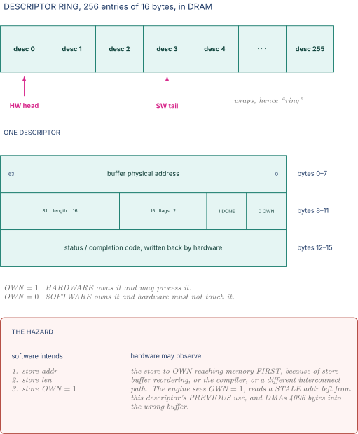
That one bit is the entire synchronization protocol between a CPU and a DMA engine. No locks, no interrupts required, and no hardware bug or software bug in the ordinary sense when it fails. Stores from a CPU are not guaranteed to become visible to other observers in program order, per Virtual Memory and Memory Ordering, and a DMA engine is another observer. On a weakly ordered architecture, which includes ARM64 and therefore every Apple SoC, the reordering is the normal case rather than an exotic one. The fix is a barrier on each side.
| PRODUCER, software handing a descriptor to hardware | |
| store desc.addr / desc.len / desc.flags | |
| ---- DMB ISHST (release) ---- <== everything above is visible | |
| store desc.OWN = 1 before anything below | |
| ---- DSB ---- | |
| store doorbell register <== tells HW to look | |
| CONSUMER, software collecting a completed descriptor | |
| load desc.OWN (spin until it reads 0) | |
| ---- DMB ISHLD (acquire) ---- <== nothing below is reordered | |
| load desc.status above the OWN load |
The producer needs release ordering so the flag is not published before the data, the consumer needs acquire ordering so the data is not read before the flag is observed. This is the classic acquire-release pair, and the descriptor ring is its canonical hardware instance.
There is a hardware obligation too, and it is the one integrators forget. The engine writes the status field and then clears OWN, two separate writes into the fabric, and if the fabric reorders them software sees OWN = 0 with a stale status. So the engine must either issue them as an ordered pair on the interface, which AXI supports within a single ID per 6.4 of Interconnect and AMBA, or wait for the status write's response first, which costs a round trip per descriptor. That belongs in the contract of 3.4, because it states the ordering the block requires from the fabric rather than one it can provide alone. The doorbell has the same character, being a posted write that completes at the CPU before reaching the device, so it must come after the release barrier or the engine wakes before the descriptor is visible.
6.4 IO coherency, what it buys and what it costs
When the engine reads memory, does it see the CPU's cached, not-yet-written-back data?
Non-coherent IO says no. The engine goes straight to DRAM and the caches are invisible to it, which pushes the whole problem onto software as explicit cache maintenance. Before setting OWN = 1 on a buffer the CPU wrote, the driver must clean, meaning write back, every line, because the dirty data is in the D-cache and DRAM is stale. After observing OWN = 0 on a buffer the device wrote, the driver must invalidate every line, because the CPU may hold stale clean copies. Cost it. A 64 KiB buffer with 64-byte lines is 1024 lines, and the full maintenance sequence including barriers runs perhaps 20 cycles per line amortized, so 20,480 cycles, which at 3 GHz is 6.8 µs against a transfer that takes 16 µs at 4 GB/s. Cache maintenance is 43 percent overhead on top of the transfer, paid by the CPU, every time. That is the good case. The bad case is a driver author who gets one of the two directions wrong, producing a corruption bug that reproduces once every few hours under specific alignment.
IO-coherent says yes. The engine's transactions enter the coherent fabric as ordinary coherent requests, snoop the CPU caches, and find the current data wherever it lives, per Cache Coherence Protocols. The driver becomes a descriptor ring and two barriers. The costs land on the fabric instead.
| Non-coherent | IO-coherent | |
|---|---|---|
| Driver complexity | high, in a corruption-bug way | low |
| CPU overhead per 64 KiB | 6.8 µs of real cycles | zero |
| Fabric requirement | none, just another DRAM client | device must be a full coherent master |
| Snoop filter | not involved | must track the device's lines |
| Device read latency | DRAM latency | DRAM latency plus a snoop lookup |
Work the snoop bandwidth, because it is the number that kills naive proposals. A device streaming 4 GB/s in 64-byte accesses generates million coherent requests per second, each needing a snoop-filter lookup, each hit generating a snoop to a CPU cluster. That is a real structural load against a filter already serving the CPUs, and a fabric sized without it will not deliver the bandwidth.
So the answer is neither always nor never, it is per client, decided in the contract of 3.4. Latency-sensitive small-transfer clients sharing pointers with an application are made IO-coherent, because removing the maintenance overhead dominates. High-bandwidth streaming clients touching data the CPU is not simultaneously using, like display scanout or a camera write path, are left non-coherent, because they would flood the snoop filter for nothing. Saying that, with the 62.5 million number, is a considerably better answer than "coherency is easier for software."
6.5 The firmware and hardware boundary
Power management is where this boundary lives most clearly, and it is where your Resource Controller work sits. Some of the controller is a hardwired state machine, some is code on a small always-on microcontroller, and the line between them is set by response time rather than taste. A state machine in the always-on domain at 800 MHz detecting a condition and asserting an output three cycles later responds in ns. A microcontroller at 200 MHz woken by an interrupt, taking roughly 400 instructions for entry, decision, and action at about 1.2 cycles each, responds in , which is times slower.
That ratio decides most of the partitioning. Two further facts finish it, that firmware needs a running clock and a powered core so it cannot be in its own wake path, and that firmware can be changed after tapeout while RTL cannot.
| Function | Where | Why |
|---|---|---|
| Droop response, adaptive clock stretch | hardware | nanoseconds, per DVFS Droop and Thermal |
| Thermal trip, emergency throttle | hardware | a backstop must work when firmware has crashed |
| Clock gating enable generation | hardware | a per-cycle decision, firmware cannot see cycles |
| Wake detection, rail sequencing start | hardware | firmware may itself be powered down |
| Which DVFS operating point to request | firmware | policy over milliseconds, and you will want to tune it |
| Idle-window prediction, race-to-idle | firmware | a heuristic that will be wrong and need changing |
| Arbitrating conflicting power requests | firmware | complex, low rate, policy-shaped |
| Workarounds for silicon bugs at bring-up | firmware | this is the whole reason firmware exists |
The last row is the strategic argument. Every chip ships with errata, and every erratum you can work around in firmware is one you do not respin for. That is why the partition puts mechanism in hardware and policy in firmware, with hardware exposing enough knobs that firmware can change the policy without changing the mechanism. A state machine with a hardcoded threshold is a liability. The same machine with the threshold in a register is an asset.
Your position on this boundary is unusual and worth using. The Resource Controller is the hardware side. Microcode is the firmware side on a different axis, and it is the same skill, implementing policy in software against a hardware mechanism you also understand.
07.Part 7, high speed IO, the shape of it
An ASIC design role names high-speed IO design and protocols, with PCIe as a plus. Learn the shape thoroughly, enough to reason and ask good questions, and say plainly that you have not designed a SerDes.
7.1 Why serial beats parallel above a few gigabits
The wrong intuition is that sixteen wires at 2 Gb/s obviously beat one wire at 2 Gb/s. The answer is skew, and the way to feel it is to work the budget at two speeds.
A parallel bus sends bits simultaneously with a clock alongside, and the receiver samples all on that clock, which works only if every bit's arrival falls inside one bit period. At 2 Gb/s per pin the unit interval is 500 ps. Setup and hold take maybe 100 ps, leaving 400 ps for every source of arrival spread, which includes on-die driver mismatch, package and PCB trace length differences, connectors, and crosstalk jitter. PCB stripline propagates at roughly 6.7 ps per millimetre, so 5 mm of length mismatch costs 33.5 ps. Against 400 ps that is 8 percent, comfortable, which is why DDR memory interfaces are parallel. Push to 10 Gb/s and the UI is 100 ps, and setup and hold do not scale proportionally, so call them 30 ps, leaving 70 ps for everything.
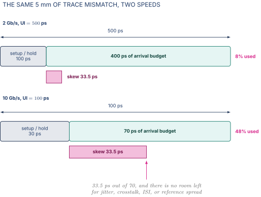
To make 10 Gb/s parallel work you would need trace matching to well under a millimetre across sixteen signals, through two packages, a connector, and a board, over temperature. Nobody can build that, and nobody tries.
A serial link makes the problem vanish by having nothing to skew against. One differential pair, no companion clock, timing extracted from the data itself. There is no bit-to-bit skew because there is only one bit at a time. What was an inter-wire matching problem that gets harder with speed becomes an intra-wire signal-integrity problem, solved with circuits rather than mechanical precision. The pin count seals it. A 16-bit single-ended bus at 2 Gb/s delivers 32 Gb/s one way and needs roughly 16 signals plus 8 ground returns plus a clock pair, about 26 pins. One serial lane at 32 Gb/s delivers the same on 2 pins per direction, so 4 pins full duplex.
7.2 Recovering the clock, fighting the channel, coding the line
Having removed the clock, the receiver must reconstruct it. Clock and data recovery is a feedback loop that locks a local oscillator to the transitions in the incoming data and produces a sampling clock centred in the eye. The loop needs transitions, and a long run of identical bits gives it no error signal at all, so its correction goes stale and its jitter grows. Practical links therefore guarantee a maximum run length, which is what line coding exists to provide.
A wire is also a low-pass filter, since skin effect in the copper and dielectric loss in the board both worsen with frequency and length. A channel with 20 dB of loss at Nyquist attenuates by , so an 800 mV swing arrives at 80 mV. That alone is survivable. What is not is that the loss is frequency dependent, so a fast alternating pattern arrives much smaller than a slow one and each bit's energy smears into the bits after it. That is inter-symbol interference, and it is the actual enemy.
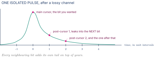
Three complementary mechanisms fix it. Transmit FFE, or de-emphasis, pre-distorts by boosting high-frequency content so the received pulse arrives clean, though since it cannot raise total transmit power it works by attenuating the easy content rather than boosting the hard content. Receive CTLE is an analog filter whose high-frequency boost inverts the channel roll-off, cheap and continuous, amplifying noise along with signal so it has a limit. Receive DFE is the clever one. Once the receiver has decided bit it knows exactly how much tail that bit contributes to the bits after it, because the tail shape is a property of the channel, so it subtracts the known contribution before deciding the next bit. Subtracting a decision rather than a signal removes ISI without amplifying noise, which is why every modern link has one. It can only cancel post-cursors, since it needs the decision first, and it propagates errors, since one wrong decision injects a wrong correction into several following bits.
Line coding supplies two properties the raw data lacks, and keeping the purposes separate is what shows understanding. Transition density, so the CDR has edges to lock to, guaranteed by bounding run length. DC balance, so the average voltage is zero over any reasonable window, required because high-speed links are AC coupled and a persistent bias toward ones charges the series capacitor until the receiver's decision threshold drifts, which is baseline wander. That one is guaranteed by bounding the running disparity, the accumulated excess of ones over zeros.
8b/10b maps every byte to a 10-bit symbol chosen so no symbol has more than five identical bits in a row and the running disparity stays within forever, both guarantees structural rather than statistical. The price is 20 percent overhead, so Gen1's 2.5 GT/s yields 2.0 Gb/s, or 250 MB/s per lane per direction. 128b/130b adds a 2-bit sync header to 128 bits of payload and leans on a scrambler, an XOR with a pseudo-random sequence, making long runs statistically unlikely rather than structurally impossible. That weaker guarantee buys an overhead of only percent, so Gen3's 8 GT/s gives Gb/s, or 984.6 MB/s per lane, which is where "roughly 1 GB/s per lane at Gen3" comes from and why a x16 Gen3 link is 15.75 GB/s.
| Generation | Signalling | Coding | Payload per lane per direction |
|---|---|---|---|
| Gen1 | 2.5 GT/s | 8b/10b | 250 MB/s |
| Gen2 | 5 GT/s | 8b/10b | 500 MB/s |
| Gen3 | 8 GT/s | 128b/130b | 985 MB/s |
| Gen4 | 16 GT/s | 128b/130b | 1.97 GB/s |
| Gen5 | 32 GT/s | 128b/130b | 3.94 GB/s |
| Gen6 | 64 GT/s, PAM4 | FLIT mode with FEC | roughly 7.5 GB/s |
Gen6 is the interesting row. It moves to PAM4, four voltage levels carrying 2 bits per symbol, so 64 GT/s comes from 32 GBd. That halves the bandwidth demanded of the channel and quarters the vertical eye opening, raising the error rate past what retry alone can absorb, so Gen6 adds forward error correction in the link layer. Spending redundancy to buy margin is exactly the subject of your NAND flash error-correcting-code work, and it is an honest bridge from your background into their domain.
7.3 Lane training and the eye diagram
A link comes up knowing nothing about itself, so bring-up negotiates everything. In PCIe the negotiating state machine is the LTSSM, going Detect, then Polling, then Configuration, then L0 for normal operation, with a Recovery state for speed changes and retraining, plus L0s, L1, and L2 low-power link states. What gets negotiated is worth listing because each item is a real hazard somebody designed around. Lane count, since a x16 slot may hold a x4 card or have a broken lane and the link must fall back. Lane reversal, because board routing is far easier if lane 0 at one end may meet lane 15 at the other. Polarity inversion per lane, because swapping P and N of a differential pair is the easiest way to shorten a trace. Speed, since the link starts at Gen1 where everything works and negotiates upward. And equalization coefficients, where at Gen3 and above the two ends iteratively exchange requested FFE and DFE settings until both are satisfied, which is why higher generations take longer to train.
The eye diagram summarizes all of it. Overlay thousands of unit intervals and what stays open in the middle is the margin, with height being voltage margin set by loss and equalization and noise, and width being timing margin set by jitter and ISI and CDR performance. The receiver must sample inside both, and a closed eye means no sampling point exists where every trajectory is on the correct side. Two facts make the picture more useful than it looks. Modern receivers sweep their own sampler in voltage and phase and count errors, producing an eye from inside the chip without an oscilloscope, which is how a shipped system diagnoses a marginal link. And the contour that matters is not "open" but "open at a specified bit error rate," typically , since that eye is meaningfully smaller than the one you see in a few seconds of capture. Asking "at what BER" when somebody shows you an eye is the question that signals you know what you are looking at.
08.Part 8, PCIe in three layers
8.1 The stack
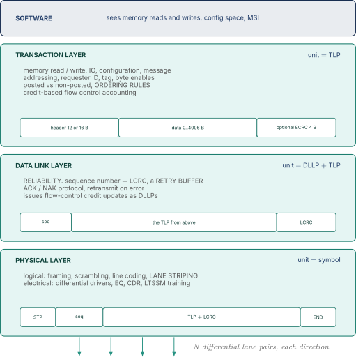
The layering is not decoration. Each layer solves one problem completely and hands a clean abstraction upward, so each can be reasoned about, verified, and debugged alone. The transaction layer never thinks about bit errors, the data link layer never thinks about addresses.
The physical layer is everything in Part 7, plus one PCIe-specific mechanism worth knowing. Lane striping means a x8 link is not eight independent streams, it is one byte stream distributed across eight lanes, so a x8 link is one logical pipe of eight times the bandwidth. That is why a x8 link losing a lane cannot run at 7/8 speed, it renegotiates down to x4, since striping needs a power-of-two lane count with defined ordering.
8.2 The data link layer
This layer exists because the physical layer is imperfect. At bit error rate a Gen3 x16 link carrying bits per second sees errors per second, roughly one every eight seconds. Uncorrected that is a corrupted memory write every eight seconds, which is not a computer. So every TLP gets a sequence number and an LCRC. The receiver checks the CRC and returns an ACK for a good packet with the expected sequence number or a NAK for a bad one. The transmitter keeps every unacknowledged TLP in a retry buffer and, on a NAK or timeout, retransmits from the failed sequence number onward. An ACK for sequence implicitly acknowledges everything up to , so acknowledgements batch.
Size the retry buffer, because that is the design question. It must hold everything sent during one round trip before an acknowledgement could return, so for a Gen3 x8 link at 7.877 GB/s with a 1 µs acknowledgement round trip that is bytes, roughly 7.9 KiB. Undersize it and the transmitter stalls waiting for acknowledgements while the wire sits idle. That is Little's law again, the same "buffering must cover the round trip" argument as the outstanding count of 3.4 and the credit sizing of 7.1 of Interconnect and AMBA, appearing here for the third time in this note. Noticing that it is the same argument every time is the point.
The layer's second job is credit-based flow control, and PCIe's version has six independent pools rather than one, being header and data credits kept separately for each of posted, non-posted, and completion traffic. Two independent reasons, and both get asked. Header against data, because a burst of 4-byte writes consumes one header credit each and almost no data, while a burst of 4 KiB writes consumes one header each and enormous data. A single combined pool lets one pattern starve the other and leaves the buffer either mostly empty or mostly stalled. Posted against non-posted against completion, because completions must always make progress, since a completion is what frees the resource a requester is holding. Sharing a pool would let an endpoint full of incoming requests block the completions that would let it drain them, deadlocking the link with no error. Separate pools break the dependency by construction, which is the same fix virtual channels apply on chip and for the same reason, per Part 4 of Interconnect and AMBA.
8.3 The transaction layer and its ordering rules
The transaction layer carries TLPs, of which the types worth naming are memory read, memory write, IO read and write, configuration read and write, and messages, with completions returned for anything needing one. The structural distinction is posted against non-posted. A memory write is posted, meaning the requester considers it complete once sent with no completion returned. A memory read is non-posted, meaning a completion carrying data must come back. Every PCIe ordering rule follows from that asymmetry, because a posted write has no return path and therefore no way to tell the sender when it landed.
| PRODUCER-CONSUMER OVER PCIe | |
| Device writes data into memory ..... posted write TLP #1 | |
| Device writes a "ready" flag ..... posted write TLP #2 | |
| CPU polls the flag, sees ready, reads the data | |
| For this to be correct, TLP #2 must not overtake TLP #1 anywhere in | |
| the fabric. If it does, the CPU sees the flag set and reads stale data. | |
| Hence THE rule: a posted write may never pass another posted write. |
| Can this... | pass a Posted? | pass a Non-posted? | pass a Completion? |
|---|---|---|---|
| Posted | No, never | Yes, and it must be allowed | Yes, and it must be allowed |
| Non-posted | No | Yes, optional | Yes, optional |
| Completion | No, by default | Yes | same ID no, different ID yes |
Read the two structural entries. Posted-cannot-pass-posted is the correctness rule that makes producer-consumer work. Posted-must-be-allowed-to-pass-non-posted is the deadlock avoidance rule, the mirror of the completion credit separation above. If a posted write could be stuck behind a read waiting for a completion, and that completion is behind the posted write elsewhere in the topology, you have a cycle. Letting the write past breaks it.
The famous practical consequence, which every driver author knows and many hardware engineers do not, is that a read flushes prior posted writes. Since a completion cannot pass a posted write, issuing a read to a device and waiting for its data guarantees your earlier posted writes to it have arrived. That is why drivers do an apparently pointless register read after writing a doorbell. It is the only way to know the write landed, because posted writes give no acknowledgement.
8.4 The vocabulary that gets asked
The root complex is the host side, integrated into the SoC, owning the address space and originating configuration cycles. An endpoint is a device, a switch fans one link into several, and the topology is a tree rather than a bus despite the historical name. At boot, enumeration walks the tree with configuration reads, discovers each device by vendor and device ID, reads its resource requirements, and assigns address ranges. How software learns a device's window size is a nice piece of first-principles cleverness.
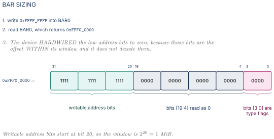
The device never reports its size. Software infers it from which bits refuse to change, then allocates a naturally aligned 1 MiB region from the map of Part 4 and writes its base into the BAR. The window is necessarily a power of two and naturally aligned because the mechanism cannot express anything else, which is the same alignment discipline 4.2 derived from decode depth, arrived at independently.
MSI and MSI-X. A legacy PCI interrupt was a wire, which does not exist over a serial link, so a PCIe interrupt is a memory write to a special address that the interrupt controller decodes. MSI allows up to 32 vectors as a power-of-two block sharing one target address with consecutive data values. MSI-X allows up to 2048 vectors held in a table in the device's own memory, with an independent address and data per vector. That independence is the whole point, since a 64-queue network device wants each queue's completions to interrupt the CPU that owns that queue, so each vector needs its own target address. MSI cannot express it, and "per-vector CPU steering for multi-queue devices" is the answer when asked why MSI-X exists.
ATS, PRI, and ACS. Address Translation Services lets a device ask the IOMMU for a translation and cache it in a device-side TLB, skipping the IOMMU lookup on subsequent accesses. Page Request Interface lets a device take a page fault, asking the host to page memory in rather than requiring the driver to pin every buffer. Together they let a device walk the same virtual address space as an application, which is what makes shared-virtual-memory accelerators possible. Access Control Services governs whether peer-to-peer traffic between two endpoints under one switch may bypass the root complex and therefore the IOMMU, which matters because bypassing the IOMMU bypasses the protection of 4.3. I/O Architecture has the depth on all four.
09.Part 9, documentation
An ASIC design role lists "Documentation and Reporting, create detailed micro-architecture and design documentation" as one of five description bullets. Five bullets is very little space, and spending twenty percent of it here is deliberate. It means the team has been burned, and it means an interviewer will probe whether you treat specifications as overhead. The correct answer is not "yes I write documentation," it is to explain what a specification is, which is the contract four other teams work from in parallel.
A microarchitecture specification covers the block's purpose and context including what it does not do and what it assumes about its neighbours, every interface with its protocol and width and timing and outstanding capability and ordering guarantees, the internal structure with a block diagram and pipeline register locations, every state machine drawn with legal transitions and defined behavior on illegal input per 6.1, the register map generated rather than hand-copied per Part 5, the performance targets with the arithmetic showing the structure meets them, clocking and power down to clamp values and the wake budget, reset and initialization including the release-order dependency and the software init sequence, every error the block can detect and what state it leaves behind, the debug counters and trace and triggers per DFT and Silicon Debug, and the verification requirements including the corner cases the designer knows are hard.
It matters because it is not read once by one person. It is the single upstream input to five parallel workstreams, so a vague specification does not cause one problem, it causes five.
| Reader | What they extract | What a vague spec costs them |
|---|---|---|
| Verification | coverage model, checkers, assertions, test plan | they verify behavior the designer did not intend, or miss behavior he did |
| Physical design | area estimate, macro list, aspect ratio, boundary budget | the floorplan of 2.4 is built on a wrong area number and is redone |
| Software and firmware | register map, programming model, init sequence, error semantics | the driver is written against a guess, found at bring-up |
| Post-silicon validation | bring-up sequence, observability points, expected signatures | first silicon arrives and nobody knows what working looks like |
| Integration | the eight rows of Part 3 | the 1.1 deadlock, six or seven times, per 1.2 |
Make the cost concrete with the smallest possible omission. The specification does not say what a read to an unimplemented offset returns. The RTL author's case default returns the last-read value, because that is what falls out of not having a default. Verification does not test it, because it is not in the specification so it is not in the coverage model. The driver author assumes reads return zero, because that was the convention on his last four blocks. Firmware uses a read of offset 0x40 as a cheap presence probe, expecting zero on absent hardware. Nothing goes wrong for a year. Then a new revision adds a register at 0x40, the probe reads non-zero on a block that is present, the presence logic inverts, the block is never initialized, and the bug appears only on one firmware and silicon combination and is not reproducible on the previous stepping. It takes a week across three teams.
One unstated sentence would have prevented it. The cost of a specification gap is not the effort to write the sentence, it is the debug time of every team that guessed differently, multiplied by the number of times the guess mattered. The corollary is that a specification is a living document, and every engineering change order that alters behavior must go back into it, or people stop trusting it, go back to reading the RTL and asking in the hallway, and you are back to 1.1.
10.Part 11, check yourself
Answer out loud, in full sentences, as if an interviewer asked. If you cannot, reread the section named.
- Two blocks each pass 100 percent of their own regressions and the chip they form deadlocks. Give a specific mechanism, say why neither testbench could have found it, and place it in the structural or behavioral class along with the tool that would have caught it. (1.1, 1.3)
- A hard macro is 2.1 mm by 1.4 mm with all its data pins on one edge. Give two separate ways its placement constrains the design before any standard cell exists, with a number on each. (2.4)
- Produce the eight-row integration contract from memory, and for four rows name the specific failure the row prevents. Two PLLs are both programmed to 800 MHz, so is a path between them synchronous? (3.1, 3.2)
- A block sits on a 128-bit AXI at 800 MHz with 120 ns round-trip latency. How many outstanding transactions does it need, and what happens if its designer implemented eight? (3.4)
- Two teams each constrain their boundary to 60 percent of the period and both close timing. Show why the chip does not, and say when it is discovered. (3.5)
- Why must every address range be a power of two and aligned to its own size? Work the decode-depth difference in gate levels. (4.2)
- Two 2 KiB register blocks share one 4 KiB page. State the security consequence and the design rule that follows. Then say what a 1 MiB aperture dropped into the middle of DRAM costs software. (4.3)
- What is the correct behavior on a read to an unmapped address, what is the failure mode if you get it wrong, and why must a secure-only range be enforced at the decoder rather than at the target? (4.4)
- Hardware sets an RW1C interrupt status bit in the same cycle software writes 1 to clear it. Which must win, and what is the failure if the other does? (5.3)
- Software reads a 64-bit counter over a 32-bit bus in two accesses. Show a value it can observe that the counter never held, give the hardware fix, and state the contract it imposes on software. (5.4)
- A device generates 500,000 events per second. Show why one interrupt per event is unworkable, then design a coalescing scheme and say which threshold binds at which load. (6.2)
- Software builds a DMA descriptor and sets its OWN bit. Describe the ordering hazard, place the barriers on both sides, and say what hardware owes in the completion direction. Then quantify what IO coherency would buy and cost instead. (6.3, 6.4)
- Where does the boundary between hardware state machine and firmware policy fall in a power controller, and what latency ratio sets it? (6.5)
- Why did multi-gigabit interfaces abandon parallel signalling? Work the skew budget at 2 Gb/s and at 10 Gb/s per pin, then name the two separate guarantees line coding supplies. (7.1, 7.2)
- Name the three PCIe layers, say what each solves, explain why completions need their own credit pool, and say why a posted write may never pass another posted write. (8.1 to 8.3)
11.Part 12, related notes
- Interconnect and AMBA for the fabric every block in Part 2 attaches to, the AXI contract of 3.4, and the deadlock argument that reappears as PCIe's separate credit pools
- Clocking Reset and Domain Crossing for the synchronizers behind the clock contract of 3.2 and the reset release and RDC material there
- Power Fundamentals and Clock Gating for domains, isolation clamp values, retention, and the sequencing the wake budget of 3.3 rests on
- STA Synthesis and Physical Design for the floorplan that hard macros constrain in 2.4 and the
set_input_delayconversation of 3.5 - Virtual Memory and Memory Ordering for the barriers that make the descriptor ownership protocol of 6.3 correct
- Cache Coherence Protocols for what an IO-coherent master actually joins in 6.4
- Arbiters FIFOs and CAMs for credit-based flow control and the depth reasoning behind the retry buffer of 8.2
- DFT and Silicon Debug for the scan and JTAG row of the contract and the observability a specification must promise
- Verification Methodology for the UVM register model generated in 5.2 and where integration tests sit in a verification plan
- DVFS Droop and Thermal for why droop response must be hardware rather than firmware in 6.5
- I/O Architecture for the vault's treatment of memory-mapped IO, DMA, the IOMMU, PCIe, ATS, PRI, and CXL
- TLBs and Address Translation for the TLB reach arithmetic driving the large-page argument of 4.3