Power Fundamentals, Clock Gating, and Power Domains
September 8, 202643 min readadvanced
In steady state exactly one of a CMOS gate's networks conducts, so no current flows. But the input ramps rather than jumps, and during that ramp there is a window where the input is above the NMOS threshold…
01.Part 1, where the power actually goes
1.1 One capacitor, and the equation that follows
Derive the famous equation rather than quoting it. It takes four lines.
From Digital Logic and Timing, a gate's output is a wire plus the input pins it drives, and together they form a capacitance . Charging from 0 to moves a charge out of the supply. The supply sits at a constant throughout, so it hands over . But the energy stored on the capacitor is only . The other half burned as heat in the PMOS resistance on the way in.
That half is not recoverable by better design. Pushing charge through any resistance into a capacitor wastes exactly half, for every resistance value. A wider transistor charges faster and burns the same total. Then the node goes low, the stored drains through the NMOS, and that half is burned too. One complete round trip costs the supply exactly , all of it heat.
Put a number on it with fF, a fair load for a small gate, and V. Then femtojoules. Absurdly small. The problem is purely one of multiplication.
Nodes do not toggle every cycle. Define the activity factor as the average number of transitions per clock cycle. Real data nodes sit between 0.05 and 0.20 once glitching is counted. The clock sits at exactly 1.0, because it rises once per cycle by definition. Multiply energy per transition by transitions per second and you have power.
For one node at , fF, V, GHz, that is . Two million such nodes is a watt. A hundred million is fifty watts.
1.2 The four levers
| Lever | Exponent | What it buys | What it costs |
|---|---|---|---|
| activity | linear | large, with no performance loss when the work was useless | design effort, small area |
| capacitance | linear | modest | smaller cells are slower, short wires need a better floorplan |
| voltage | squared, effectively cubed | enormous | frequency must fall with it, and there is a hard floor |
| frequency | linear | proportional, and you lose the performance | performance, one for one |
Frequency alone is a bad lever. Halving halves power and halves performance, so the energy to finish a fixed job is unchanged. You spread the burn out, you do not reduce it. Frequency only becomes real when it drags voltage down with it, which is DVFS Droop and Thermal.
Activity is the free lever. If a register holds a value nobody will change this cycle, clocking it accomplishes nothing, and stopping that clock costs zero performance. That is why Parts 2 through 5 are all about .
1.3 Short-circuit power
In steady state exactly one of a CMOS gate's networks conducts, so no current flows. But the input ramps rather than jumps, and during that ramp there is a window where the input is above the NMOS threshold and below the PMOS turn-off point. Both devices are partly on and current flows straight from supply to ground doing no work.
With V and both thresholds at 0.3 V, both conduct while the input is between 0.3 V and 0.6 V. If the input takes 20 ps to swing the full rail, it spends roughly ps in that window on every transition.
The loss is proportional to the input slew rate, so a gate fed a lazy edge burns far more than the same gate fed a sharp one. In a well-constrained design this is five to fifteen percent of dynamic power, and what keeps it there is the maximum-transition constraint in synthesis. That is part of why set_max_transition exists. The counterintuitive consequence is that upsizing a driver often reduces total power at the gates it feeds, because the sharper edge cuts their crossover current, even though the bigger driver presents more capacitance itself.
1.4 Leakage, and why it forced power gating into existence
Everything above happens only when something switches. Leakage happens whenever the chip has power at all.
The dominant mechanism is subthreshold conduction. A transistor below threshold is not off, its current merely falls exponentially as , where mV at room temperature and . That exponential has a practical form. The subthreshold slope, meaning how much gate voltage you must remove to cut current tenfold, is
Now the number that explains twenty years of industry history. Lowering by 78 mV multiplies leakage by ten. Not by ten percent, by ten. And must come down when comes down, because gate speed depends on the overdrive . That is the trap. Scaling supply voltage to save dynamic power forces threshold voltage down, which multiplies leakage exponentially, which eventually eats the saving. This is why Dennard scaling ended around 2005 and clock frequencies stopped climbing.
A second mechanism, gate leakage, is electrons tunnelling through the gate oxide. It became severe as oxides thinned to a few atomic layers and was largely fixed by high-k dielectrics with metal gates around 45 nm, which allowed a physically thicker insulator with the same electrical effect.
Leakage also rises steeply with temperature, roughly doubling every 10 degrees Celsius. Even a conservative version is dramatic. A block leaking 3 W at 50 C, at a factor of 1.7 per 10 degrees, leaks W at 90 C. That feedback path is the thermal runaway mechanism in DVFS Droop and Thermal.
| Era | Rough leakage share of total power | Consequence |
|---|---|---|
| 180 nm, late 1990s | under 5 percent | clock gating alone is sufficient |
| 90 nm, mid 2000s | 15 to 25 percent | leakage becomes a budget item, multi-Vt becomes standard |
| 45 nm, high-k metal gate | partially recovered | gate leakage solved, subthreshold still growing |
| FinFET generations | 20 to 35 percent when hot | power gating becomes mandatory |
Those are order-of-magnitude public figures and vary enormously with process and temperature. The causal chain is what matters, and it answers "why do we need power gating if clock gating already exists" in one sentence. Clock gating stops switching. It does not remove supply. Leakage does not care whether anything is switching. So once leakage became a large fraction of total power, a technique that removes supply entirely became necessary.
02.Part 2, the clock network is the biggest single load
2.1 Count it rather than assert it
The claim that the clock burns a quarter to a third of dynamic power is repeated constantly and almost never justified. Justify it once and the number is yours.
Take a block with 100,000 flip-flops and about twenty combinational nodes per flop, at 0.9 V and 3 GHz. Each flop presents roughly 2 fF at its clock pin, and the tree buffers and wires delivering the edge add about as much again, so call it 3 fF effective. Combinational nodes drive longer wires, so call those 2 fF at .
| Contributor | Nodes | Cap each | Total | Power | Share | |
|---|---|---|---|---|---|---|
| clock tree plus flop clock pins | 100,000 | 3 fF | 300 pF | 1.00 | 0.73 W | 33 percent |
| combinational logic | 2,000,000 | 2 fF | 4 nF | 0.15 | 1.46 W | 67 percent |
Checking the clock row, W. One third, from first principles.
Look at why and it stops being surprising. The clock loses badly on capacitance, 300 pF against 4 nF. It wins all of that back on activity, 1.00 against 0.15, and on the fact that its capacitance is unavoidable and always present. A small network that never rests beats a huge one that mostly does.
2.2 A flop that never changes still burns clock power
Consider a configuration register written once at boot and holding the same value for eight hours. Its never changes, its never changes, nothing downstream toggles. Its data-side activity factor is zero.
Its clock activity factor is still 1.0. Every rising edge charges the clock pin, toggles the flop's internal clock buffers, and flips the master and slave latch clocks, all to recapture a value already there. A typical flop burns 30 to 60 percent of its total power on the clock pin when its data is idle. That is the target. Clock gating is not mainly about the flop's data-side power, it is about not paying for edges that accomplish nothing.
03.Part 3, clock gating
3.1 The naive AND gate, and exactly how it fails
The idea is one sentence. If a group of registers will not change state this cycle, do not deliver a clock edge to them. You already wrote the condition, since always_ff @(posedge clk) if (en) q <= d; says precisely when the register updates. Without gating that en becomes a mux at the flop's input feeding back to itself, and the flop is clocked every cycle to recapture what it already had.
The obvious implementation is an AND gate on clock and enable. It is broken, because enable is a data signal produced by combinational logic, which from Digital Logic and Timing glitches on its way to the right answer and settles somewhere in the middle of the cycle. It does not politely change only while the clock is low.
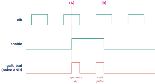
Event (A). The enable rises while the clock is already high, so the AND output jumps to 1 and every flop downstream sees a rising edge in the middle of the high phase. That is a real clock edge as far as they are concerned. They capture whatever is on at that instant, which is a half-settled glitch value, exactly the adder-at-5-ns situation from Digital Logic and Timing. Garbage enters the registers and nothing flags it.
Event (B). The enable falls while the clock is high, so the AND output drops early and truncates the pulse. The flops get a runt pulse, a high phase far shorter than they were characterized against. This is worse, because a flop given a too-narrow pulse may capture, may not capture, or may go metastable and hold an undefined voltage for an unbounded time, which is the failure mode in Clocking Reset and Domain Crossing.
Both failures depend on exactly when a combinational signal settles, so they are timing, temperature, and silicon dependent, and essentially impossible to debug afterwards. Say it in one sentence. The enable is a data signal that can change at any point in the cycle, and any change during the clock's high phase produces either a spurious edge or a runt pulse.
3.2 The integrated clock gating cell
If the problem is the enable moving while the clock is high, hold the enable still while the clock is high. That is exactly what a level-sensitive latch does, and it is why a latch appears in a design otherwise built entirely from flip-flops.
The device is the integrated clock gating cell, or ICG. It is a single characterized standard cell rather than something you assemble, because the internal timing between latch and AND must be guaranteed by the library vendor and not left to synthesis.
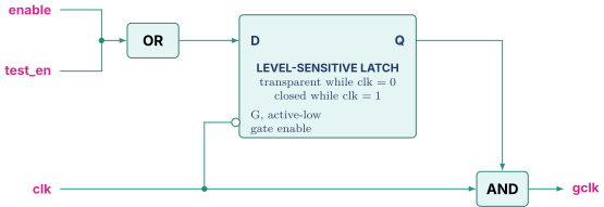
Same stimulus as before, now through the ICG.
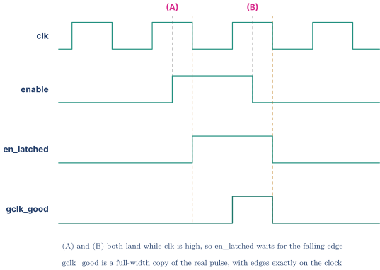
The mechanism in one paragraph. The latch is transparent while the clock is low and closed while it is high, so the latch output can only change during the low phase. During the low phase the AND's other input is 0, pinning gclk to 0 regardless of what the enable does, so all glitching is invisible. When the clock rises the latch snaps shut, freezing the enable for the entire high phase, so the AND sees a rock-solid enable across the whole window. The gated clock's rising edge is therefore exactly the real rising edge and its falling edge exactly the real falling edge. It is either a perfect copy of the pulse or nothing.
Two follow-ups get asked. Why low-transparent? Because the gating element is an AND feeding positive-edge flops. To gate a clock feeding negative-edge flops the gating element is an OR, which pins the output to 1 while the clock is high, so the latch must be high-transparent to be closed during the low phase. The rule is that the latch must be closed during whichever phase the gating element is not already forcing. Why is test_en there? Scan shift requires every flop to be clocked, and the functional enable will be low for most gaters most of the time, so asserting test_en forces every gater on. Forgetting to connect it produces unreachable scan chains at DFT signoff, per DFT and Silicon Debug.
3.3 Fine grained and coarse grained
Fine-grained gating stops the clock to one register or a small group, driven by that register's own functional enable. Synthesis inserts nearly all of it automatically, since a conditional assignment hands the tool the enable expression. Coarse-grained gating stops the clock to a whole unit, driven by architectural knowledge that the unit is idle. Somebody has to write the idle detection and be certain it is right.
Coarse gating saves far more for a structural reason, not a matter of degree.
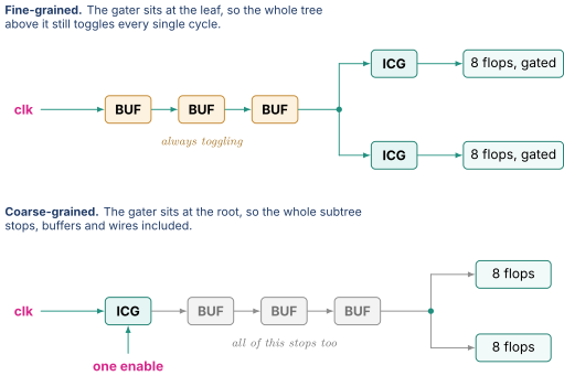
The tree buffers and the wire between them are a large fraction of the 300 pF from 2.1. Fine gating removes the flop clock pins from the bill, coarse gating removes the pins and the tree feeding them. A real design wants both, with the coarse gater upstream of the fine ones, and they compose without conflict because AND-ing twice is still an AND. The risk profile differs sharply. Fine gating is low risk because the tool proved the enable. Coarse gating is real risk, because a wrong idle condition silently loses state updates.
3.4 Clock gating efficiency, defined honestly
Three different things get called clock gating efficiency and they give different numbers on the same design.
Flop coverage is the fraction of flops with a gater in front. Weakest, because it counts a gated 4-flop group and a gated 64-flop group equally and says nothing about whether the enables are ever low. Clock-power-weighted coverage is the fraction of clock switching power downstream of some gater, which is better because it gives a coarse gater proper credit for its subtree, but it is still a static structural measure that tells you what could be saved, not what is. Dynamic gating efficiency simulates a real workload and counts flop-clock-cycles actually suppressed as a fraction of those that would have occurred ungated. Measured, workload dependent, and the one worth quoting because it corresponds to power on the bench.
The resume number is the dynamic one, and the honest framing is that 95 percent of the clock-power-weighted flops sit behind a gater whose enable comes from a real idle or update condition, measured across the regression workload set. A number quoted without naming both the definition and the workload is not a number, and saying so unprompted is itself a good signal.
Now the part that separates people who ran the flow from people who read about it. Coverage is not savings. Ungated clock power in 2.1 was 0.73 W. Suppose the gated flops, representing 95 percent of clock power, have enables low on average 70 percent of cycles.
Clock power falls from 0.73 W to about 0.25 W plus gater overhead. Against 2.19 W of total block dynamic power that is a 22 percent cut. Ninety-five percent coverage did not save ninety-five percent of anything, and being able to say that with the arithmetic is far more convincing than the headline.
04.Part 4, the four follow-ups on the 95 percent
4.1 How the ungated logic was found
Start from the power tool's per-instance report, generated on a gate-level netlist with switching activity from a real workload simulation, usually SAIF or FSDB. It gives every register's clock power, data power, gated status, and toggle rate. Sort descending by clock power, filtered to ungated instances. That list is the work queue and it is short, because power distribution is heavily skewed and a handful of wide register banks hold most of the recoverable power.
For each entry ask one question. Does a correct enable condition exist, and can it be expressed cleanly in RTL? If yes the fix is an RTL change rewriting the register as a conditional assignment so synthesis gates it automatically. If no, either because the register genuinely updates every cycle or because deriving the condition costs more than it saves, close the entry with a reason so it does not come back.
The second, coarser pass looks at whole blocks. Take a workload trace, find windows where a unit has nothing in flight, and check whether a coarse gater covers it. That is where the large wins are, and it is a microarchitecture conversation rather than an RTL cleanup.
4.2 Why synthesis missed some
Synthesis gates only when it can prove an enable exists, and there are several ways to hide one.
The enable was a mux rather than a conditional. q <= sel ? a : q is a recognizable hold. q <= mux_out where mux_out happens to equal q under a condition several logic levels away is not, because proving it needs reasoning the tool does not attempt. Most common cause, and the fix is an RTL rewrite.
The enable logic was timing-critical. This is the best answer to give, because it shows you know where the ICG sits. The gater is placed upstream in the clock tree relative to the flops it gates, while the enable is launched by a flop sitting downstream in that same tree. So the clock reaches the launching flop later than it reaches the ICG. That is negative skew on the enable path in exactly the sense of section 6.2 of Digital Logic and Timing, and it subtracts from the enable's setup budget. With 200 ps of tree insertion delay and a 333 ps period at 3 GHz, most of the budget is gone before the enable logic gets a single gate. Synthesis declines to gate rather than break timing, and it is right to.
The remaining causes are that the group was too small to pay for itself, which 4.3 quantifies, that the register sits in a synchronizer or domain crossing where gating is forbidden rather than merely unprofitable, and non-standard coding such as accidentally inferred latches or multiple always blocks driving one register.
4.3 What it costs in area, timing, and skew
Area. An ICG has a latch, an OR, and an AND inside, typically four to eight gate-equivalents, plus routing for its enable.
Its own power. This is the cost that decides everything. The ICG's clock input is on the free-running clock, so it toggles every cycle whether or not it gates anything, costing roughly one to two flop clock loads permanently. Let that cost be flop loads, and let it gate flops idle a fraction of cycles. It saves and costs always, so it pays only when , meaning .
| Idle fraction | Minimum group size to break even |
|---|---|
| 0.9, mostly idle block | 3 flops |
| 0.5 | 4 flops |
| 0.25 | 8 flops |
| 0.10, busy datapath | 20 flops |
That is why synthesis exposes a minimum-group-size knob and why the sensible setting is not a constant. A rarely-used configuration block wants a small threshold, a hot datapath wants a large one. Setting it globally to 4 and walking away leaves power on the table in one place and burns it in another.
Timing and skew. The ICG sits on the clock path, so it adds insertion delay. The gated branch now arrives later than ungated branches, and clock tree synthesis must match it or accept skew, which from section 6.2 of Digital Logic and Timing moves setup and hold in opposite directions. Going from 60 to 95 percent coverage inserts many more gaters, meaning many more endpoints with extra insertion delay to balance, which makes clock tree synthesis meaningfully harder and pushes hold-fix buffer counts up. Naming that cost is what makes the 95 percent claim credible rather than boastful.
4.4 What breaks
Synchronizers and clock domain crossings. A two-flop synchronizer resolves metastability by giving it two full destination-clock cycles, which requires the destination clock to be running. Gate it and a request from another domain sits in the first flop forever. If the gating enable is itself derived from that handshake you have built a deadlock, where the domain will not wake because the request cannot arrive and the request cannot arrive because the domain is asleep. The wake path must be on an always-running clock or must be asynchronous, per Clocking Reset and Domain Crossing.
DFT. Scan shift needs every flop in the chain clocked, so every ICG's test enable must be wired to scan control and asserted during shift. One gater with an unconnected or wrongly-polarized test enable breaks the whole chain it sits on, appearing as a block of untestable flops in the ATPG coverage report.
Reset. Synchronous reset only takes effect on a clock edge, so a gated block will not reset. Either the enable is forced on during reset, or the block uses asynchronous reset with its own release-timing problem from Clocking Reset and Domain Crossing.
Debug and X-propagation. Gated blocks stop advancing, so counters, trace buffers, and watchdogs inside them stop too, and a debugger halting the machine finds stale state. Separately, an incorrectly gated block holds old values that in simulation may be X, and those X values propagate outward and are hard to trace back to a missing clock edge.
05.Part 5, data gating and operand isolation
Clock gating stops registers from being clocked. It does nothing about combinational logic, which toggles whenever its inputs toggle regardless of whether anyone wants the result.
A 64-bit multiplier sits on an execution port. This cycle the port issues an integer add, so the multiplier's result will be discarded. But its operand inputs are wired to the register file read ports, which are presenting the add's operands. Those bits differ from last cycle's, so the entire multiplier toggles. Booth encoders fire, the whole compression tree from Arithmetic Hardware ripples, the final carry-propagate adder settles, and a result appears on a wire feeding a mux that ignores it. Burning a large multiplier's full switching energy for a number nobody reads is one of the biggest single wastes in an execution unit.
Data gating, also called operand isolation, holds the operand inputs stable when the result is not needed.
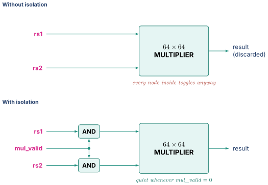
With mul_valid low both operands are forced to all zeros, they stay all zeros next cycle, so nothing inside changes and nothing toggles.
Three implementations with different costs. AND or OR gates are one extra gate per operand bit, cheapest, but they add a gate delay directly in a datapath that is often critical. The choice between them is not arbitrary, since all-zeros into a multiplier is ideal because zero partial products propagate nothing, while all-zeros into a subtractor may cause more internal toggling than all-ones. A transparent latch holds the previous operands rather than forcing a constant, avoiding a forced transition when isolation engages, at the cost of area and the latch's own timing complications. Reusing an existing pipeline register is the best answer when it applies, because if the operands already pass through a pipeline flop, clock-gating that flop with the same condition gives operand isolation free with zero added datapath delay. Reach for that first.
Isolation costs area and, in the gate cases, one delay paid on every operation including the ones that use the block. So the test is a ratio. It pays when the block is large and often idle. A 64-bit multiplier, a divider, an FPU, a large CAM, or a wide vector lane all qualify. A 3-bit incrementer does not. The dividers of Arithmetic Hardware are the extreme case, being enormous, iterative, and used on a small fraction of instructions, so they are almost always operand-isolated, clock-gated, and often power-gated too.
06.Part 6, attacking leakage
Everything so far attacked . A clock-gated flop is still powered, and a leaking transistor does not care whether its clock runs.
6.1 Multi-threshold cells
From 1.4, leakage falls tenfold for every 78 mV that threshold voltage rises. Libraries ship the same logical cell at several thresholds. If standard-Vt is mV, then high-Vt at 480 mV leaks about ten times less and is perhaps 15 to 25 percent slower, and low-Vt at 320 mV is the reverse.
Now recall the central fact from Digital Logic and Timing. Only the critical path sets the frequency. Every path with positive slack is already running faster than it needs to. So use low-Vt only where the speed is needed, high-Vt everywhere there is slack, and let synthesis place the boundary by swapping cells during optimization. The payoff is large because slack is heavily skewed. Well under ten percent of cells in a typical block sit near critical, so ninety percent or more can be high-Vt and leak a tenth as much. Nearly free, fully automated, universal practice, and the cheapest answer available when asked how you would cut leakage, so lead with it.
6.2 Power gating with sleep transistors
The heavy tool. Cut supply to the block entirely using large transistors in series with the rail.
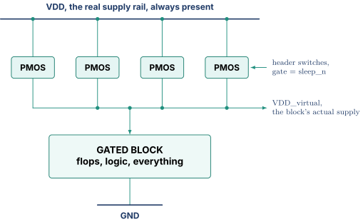
A header is a PMOS between the real supply and the block's virtual supply, as drawn. A footer is an NMOS between virtual ground and real ground. Headers are more common because cutting the supply rail directly keeps the block's ground reference intact, though footers are smaller for the same on-resistance since NMOS carries more current per unit width.
Four costs, and listing all four separates having built this from having read about it. State is lost, since every flop and every SRAM bit not on a separate always-on supply is gone. The switches have resistance, sitting in series with the whole block's supply and carrying its full current, so they must be enormous to keep the IR drop small. That is real area, often several percent of the gated block, and the residual drop eats timing margin because the block runs slightly below nominal. Designers size the network against a target virtual-rail droop of a few tens of millivolts at peak current. Entry and exit take time, microseconds typically, because the block's entire supply capacitance must be discharged and recharged. And turning it back on causes inrush current.
6.3 Inrush current and the break-even idle time
When the switches turn on, the virtual rail is at zero and the block's whole supply capacitance, including every decoupling capacitor inside it, must charge from the real rail. Charging a large capacitance quickly means a very large current, briefly. Turn the whole network on in one cycle and you can pull an amp or more for a few nanoseconds.
That current comes through the package inductance, and from DVFS Droop and Thermal a large through an inductance produces a voltage droop. The droop is not confined to the waking block. It appears on the shared rail and hits every other block on it, including cores running perfectly happily that now find themselves briefly below their minimum operating voltage. Waking one idle block can crash a different, unrelated core.
The fix is to ramp rather than switch. The sleep transistors form a daisy chain, with a small weak switch turning on first to begin charging slowly and the large switches following in sequence as the enable propagates through deliberately delayed buffers.

The rail comes up over hundreds of nanoseconds instead of a few, and falls by the same factor. The ack at the end proves the enable reached the last switch, which is a cheap and reliable indication that the rail is up.
Now the break-even. Gating costs a fixed energy to enter and exit and saves leakage power for as long as the block stays off, so it pays only if the idle window exceeds . With 50 nF of block supply capacitance at 0.9 V, recharging costs nJ, so call total overhead 60 nJ. If the block leaks 30 mW,
An idle window of 500 ns should be clock gated only. One of 50 microseconds should be power gated. Making that decision at runtime with imperfect knowledge of how long the idle will last is a central job of a power management controller, and exactly what a Resource Controller implements.
6.4 Retention
A core that loses its architectural registers must be re-initialized by software, which is slow and visible. A retention flop is a normal flop with a small always-on latch alongside, called the shadow or balloon latch, powered from an always-on rail.
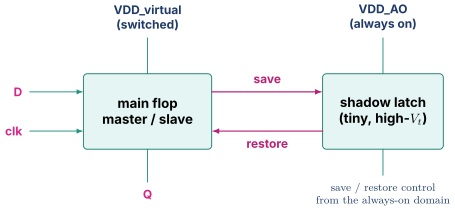
On the way down a save pulse copies the value into the shadow latch. Power goes away and the main flop loses its value, but the shadow latch keeps the bit at a tiny leakage cost. On the way up, once the rail is stable, a restore pulse copies it back.
The costs are concrete. A retention flop is perhaps 20 to 40 percent larger than a plain one, so designs retain selectively, keeping architectural state and dropping recomputable state. A separate always-on rail must be routed into the gated block, complicating the power grid. And the save and restore controls must be sequenced exactly right relative to power, because a restore issued before the rail is stable reads the shadow latch through a partially powered path and can corrupt the very value it was protecting. The alternative, software-managed save and restore to memory, needs no extra silicon and much more time, so it is right for deep infrequent sleep states and wrong for the fast idle transitions a core makes thousands of times a second.
07.Part 7, power domains and the cells at the boundary
7.1 Domains and voltage islands
A power domain is a set of instances sharing a supply and a power state, so they turn on and off together and scale voltage together. A voltage island is the physical region implementing one, with its own supply grid, its own well taps, and a boundary placement must respect. A modern SoC has many, including an always-on domain holding the power controller and wake logic, one per CPU cluster, and separate ones for GPU, neural engine, display, and IO.
The moment there is more than one domain there are signals crossing between them, and those crossings need special cells for two completely different physical reasons. Confusing the two is a common stumble.
7.2 Level shifters, and why a direct connection burns static current
Take a signal driven at 0.6 V and wire it directly into a gate powered at 1.0 V.
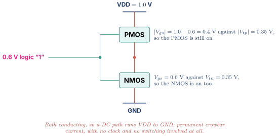
Work the arithmetic. The receiving PMOS sees a gate-to-source magnitude of V against a threshold magnitude of 0.35 V, so since it is on, weakly but genuinely. The NMOS sees V against 0.35 V, so it is on strongly. Both conduct and a permanent DC path exists.
That is a steady-state short, not a glitch and not a timing problem. It burns current every nanosecond the signal sits at logic 1, whether or not anything switches, in every gate on every crossing signal. At 50 microamps per gate across ten thousand crossings that is W of pure waste, plus a logic-level margin that is uncomfortably small and degrades with temperature.
A level shifter, usually a cross-coupled pair, produces a full-swing output in the receiving domain so the receiving gate always sees a solid 0 or a solid 1.0 V. Three practical facts get asked. Shifters are directional, so one installed backwards does not work. A low-to-high shifter needs both supplies routed to it, which constrains placement to a strip along the boundary. And high-to-low is the easier direction, since a 1.0 V signal already clears the 0.6 V domain's thresholds, though a down-shifter is still typically inserted to control overdrive on the receiving gate's thin oxide.
7.3 Isolation cells and floating inputs
Different problem, different cell. When a domain is powered off, its output drivers have no supply. They do not drive 0 and they do not drive 1, they float, drifting toward whatever leakage and coupling from neighbors put on them, typically around mid-rail.
Mid-rail is the worst possible value, because a receiving gate in the powered domain now has an input halfway between its thresholds, which turns both transistors on and produces exactly the crowbar current of 7.2, and produces an output that is neither a logic 0 nor a logic 1. That indeterminate output feeds the next gate, which is now also undefined, and corruption spreads into logic that is perfectly healthy. If the corrupted logic is the always-on power controller, its state machine goes undefined and the block responsible for turning the sleeping domain back on is itself broken. The chip hangs and only a full reset recovers it.
An isolation cell is a clamp sitting in the receiving, powered domain, forcing the incoming signal to a known constant whenever its enable is asserted.
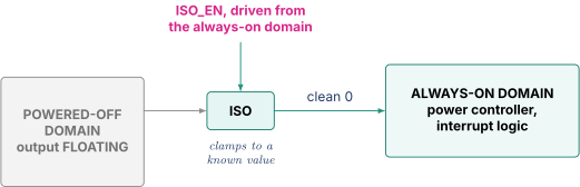
The clamp value is a design decision, not a default. A request clamps to 0 so nothing appears to be requesting. A ready or idle usually clamps to 1 so the system sees the block as available. An active-low error_n clamps to 1. Choosing wrong is a functional bug that only appears when a domain powers down. The enable itself must be driven from the always-on domain, since a clamp controlled from the domain being powered down would itself float.
7.4 Power sequencing, and what breaks at each step
This is the heart of what a power management controller does. Every step exists because omitting it breaks something specific.
| Step | Powering DOWN | What breaks if skipped or done later |
|---|---|---|
| 1 | Quiesce, stop new transactions and drain outstanding | an in-flight bus transaction is abandoned, the fabric waits forever for a response, the interconnect deadlocks |
| 2 | Clock gate the domain | state keeps advancing while you save it, so the saved value does not match what the system believes |
| 3 | Assert isolation | outputs float the instant power goes, crowbar current flows in receivers, X propagates into the always-on controller |
| 4 | Assert retention save | architectural state is lost and the block must be fully re-initialized on wake |
| 5 | Assert reset, if the design resets on entry | doing it before save destroys the state you meant to keep |
| 6 | Turn off the sleep transistors | nothing, this is last by construction |
| Step | Powering UP | What breaks if skipped or done earlier |
|---|---|---|
| 1 | Turn on the sleep transistors, staged along the daisy chain | all at once gives the inrush of 6.3 and browns out neighboring blocks |
| 2 | Wait for the rail, confirmed by the chain acknowledge | a restore or reset release into a half-charged rail is undefined |
| 3 | De-assert retention restore | restoring into an unstable rail corrupts the retained value, skipping it leaves random power-up values |
| 4 | Release reset, synchronously to the domain clock | asynchronous release near a clock edge causes recovery and removal violations and metastability, see Clocking Reset and Domain Crossing |
| 5 | Ungate the clock | the domain cannot advance and any synchronizer inside never resolves |
| 6 | Release isolation, last | the classic bug, described below |
| 7 | Un-quiesce and allow traffic | traffic arrives at a block not yet ready to answer |
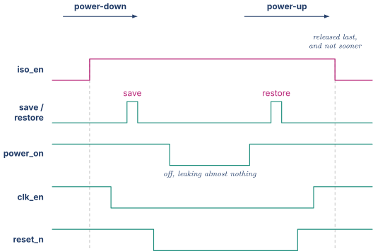
What breaks if isolation releases early. Release it at step 2, right after the rail comes up, instead of at step 6. The domain has power but its flops have not been restored and its reset has not been released, so their outputs are whatever the power-up transient left, effectively random and in simulation X. Those values are visible to the always-on domain, which is live and clocking. A spurious request asserts and the interconnect starts a transaction into a block that is not ready. A spurious interrupt fires. A state machine in the always-on controller takes a transition it should never take, and since that controller runs the rest of the sequence, the wake-up itself fails.
Memorize the rule in this shape. Isolation is the first thing asserted on the way down and the last thing released on the way up. It brackets everything else, because it is the only thing standing between an unstable domain and the rest of the chip.
Every switchable domain implies an always-on partner holding the wake detection, the interrupt path that can wake the domain, the sleep transistor control, the isolation enables, and the retention controls. Always-on logic leaks all the time by definition, so it is kept deliberately small and built from high-Vt cells wherever timing permits.
08.Part 8, power intent and why RTL cannot express it
8.1 The gap, and what UPF holds
Write the most careful SystemVerilog you can and there is still no way to say "this block's supply can be removed." RTL has no concept of a supply. A module has ports, wires, and logic, and a simulator evaluates it forever regardless of what any power controller thinks. There is no syntax for a power domain, none for "insert a level shifter here," none for "this flop retains across a power cycle."
That is deliberate separation. The same RTL should be implementable with one power domain or with six, and hard-coding domain structure into RTL would destroy that reuse. So the power architecture lives in a separate file read alongside the RTL by every tool. The standard is UPF, Unified Power Format, standardized as IEEE 1801. The older Cadence-originated alternative is CPF. UPF has effectively won and is the one to name.
A UPF file is a Tcl script declaring:
- Supply nets and ports, the actual rails, including which are always on
- Power domains, each naming its member instances and its primary supply
- Power switches, the sleep transistors, their control, and their acknowledge
- Power states, the legal combinations, so tools know "CPU off while L2 on" is legal and something else is not
- Isolation strategies, which signals crossing which boundary need clamping, to what value, under which enable and polarity
- Level shifter strategies, which crossings need shifting and in which direction
- Retention strategies, which registers retain, on which supply, with which save and restore controls
Every tool consumes the same file. Synthesis inserts the isolation cells, level shifters, and retention flops it demands. Place and route honors the boundaries and builds the separate grids. Static timing analyses each domain at its own voltage. Simulation models power behavior. One source of truth, many consumers.
8.2 Power-aware simulation, and why ordinary simulation cannot find these bugs
Ordinary RTL simulation has no notion of supply. Run the full regression on a design with six domains and the simulator happily simulates all six, all the time, forever. Power down a domain in your test and nothing happens, because "power down" is just a signal going low and the simulator has no idea it means anything. The block keeps computing and its outputs stay valid. Every missing isolation cell, every wrongly sequenced retention control, and every read of a register in an off domain passes. The bug class is invisible not because the tests are weak but because the model cannot represent the failure.
Power-aware simulation fixes the model by reading the UPF alongside the RTL. It corrupts logic in an unpowered domain to X. It models isolation, so a properly isolated output emits its clamp value while a missing cell lets X escape. It models retention, so retained flops survive the power cycle and non-retained ones come back X. It models level shifters and flags a crossing with none. And it checks the power state table, flagging a transition the UPF says is illegal. Now the bugs become visible in the most useful way, because X propagates. A missing isolation cell shows up as X arriving at the always-on controller a few cycles after power-down, which is loud and traceable.
Two honest caveats worth raising unprompted. RTL X semantics are optimistic in places, most famously that a case with an X selector may take no branch in RTL while the synthesized gates take a definite and possibly wrong one, so RTL power-aware simulation can miss bugs that gate-level power-aware simulation catches. And it only exercises the sequences your tests drive, so it needs directed tests walking every legal power state transition, ideally with coverage on the power state table itself.
8.3 Static checks
Simulation finds only what you stimulate. Static power intent checkers analyse netlist and UPF structurally and catch crossings with a missing or wrongly-directional level shifter, isolation enables sourced from a domain that can itself power off, isolation cells on the wrong side of the boundary, retention controls not on an always-on supply, always-on cells accidentally placed inside a switchable region, and internally inconsistent power state tables. None of that needs a test to hit it.
The pairing to state is that static checks prove the structure is right and power-aware simulation proves the sequencing is right, and you need both because neither finds the other's bugs.
09.Part 10, check yourself
Answer out loud, in full sentences, as if an interviewer asked. If you cannot, reread the section named.
- Derive from charging a single capacitor. Where does the factor of one half go, and why can a better transistor not recover it? (1.1)
- Rank the four levers in the dynamic power equation and say why frequency alone is a bad one. (1.2)
- What causes short-circuit power, and why does upsizing a driver sometimes reduce total power? (1.3)
- What is the subthreshold slope, what is its value, and what does it say about lowering by 80 mV? Connect that to why frequency scaling stopped. (1.4)
- Give the causal chain from process scaling to why power gating became necessary when clock gating already existed. (1.4)
- Justify the claim that the clock network is a quarter to a third of dynamic power. Why does it win despite having far less capacitance than the logic? (2.1)
- Draw the naive AND-gate gater and describe both distinct failures when the enable changes during the high phase. Which is worse and why? (3.1)
- Draw an ICG. Explain precisely why the latch must be closed during the high phase, and say what changes for negative-edge flops. (3.2)
- Give three definitions of clock gating efficiency, say which is worth quoting, and explain why 95 percent coverage is not 95 percent power saved. (3.4)
- Your coverage went from 60 to 95 percent. What did it cost? Answer in three parts, area, its own power with the break-even arithmetic, and timing and skew. (4.3)
- Why does synthesis sometimes refuse to gate a register that clearly has an enable? Give the clock-tree-skew reason specifically. (4.2)
- Name two things that break outright if you gate the wrong clock, and explain the synchronizer deadlock. (4.4)
- What is operand isolation, and what is the version that costs no extra datapath delay? (5)
- Explain why a 0.6 V signal wired into a 1.0 V domain draws static current, working the threshold arithmetic. Then say why isolation cells solve a completely different problem. (7.2, 7.3)
- Give the full power-down and power-up sequences and say exactly what goes wrong if isolation releases early on the way up. (7.4)
- Why can ordinary RTL simulation never find a missing isolation cell no matter how good the tests are, what finds it instead, and what is one limitation of that method? (8.2, 8.3)
10.Part 11, related notes
- DVFS Droop and Thermal for voltage and frequency scaling, di/dt, and the thermal feedback loop that 1.4's temperature dependence sets up
- Digital Logic and Timing for the delay model, the latch behavior the ICG depends on, and the skew analysis behind the ICG enable path problem
- Clocking Reset and Domain Crossing for why gating a synchronizer's clock deadlocks, for reset release timing, and for glitch-free clock muxing
- SRAM Arrays and ECC for the array voltage floor that limits how far a domain's voltage can drop before bit cells fail
- DFT and Silicon Debug for scan chains, the ICG test enable, and why an off domain cannot be tested
- Verification Methodology for where power-aware simulation and formal power-state checking sit in a verification plan
- From Logic to Silicon for the vault's circuit-level treatment of CMOS power
- Power, Frequency, and Thermal for the vault's architectural treatment including Dennard scaling and dark silicon