SRAM Arrays, Register Files, and Error Correction
September 8, 202696 min readadvanced
Everything else in your block is soft. A path is too slow, so synthesis upsizes a cell, restructures a tree, or place and route shortens a wire. A block is too big, so the tool remaps to smaller cells. That…
01.Part 1, why an RTL engineer has to know the circuit
1.1 The array is the one thing you cannot re-synthesize
Everything else in your block is soft. A path is too slow, so synthesis upsizes a cell, restructures a tree, or place and route shortens a wire. A block is too big, so the tool remaps to smaller cells. That elasticity is the whole reason RTL is a productive way to design.
The array has none of it. An SRAM macro arrives as a hard block with a fixed pin list, a fixed physical outline, fixed timing arcs, a fixed set of legal configurations, and a fixed minimum cycle time. Synthesis will not touch it. Place and route drops it as a rectangle and routes around it. If the macro needs 420 ps to produce data, your block runs no faster than 420 ps no matter how good the rest of your RTL is.
So the array is a fixed point, and the rest of the design bends around it. That inverts the usual mental model. You do not write RTL and then see what timing says. You read the macro datasheet first, decide what fits in a cycle before and after it, and then write RTL that lives inside that budget.
1.2 The datasheet, and the decisions it makes for you
A memory compiler is a program from the foundry or an IP vendor that takes a few parameters and emits a characterized macro plus its models. Here is what it hands back, with a plausible set of numbers for a small array in a modern process, and what each line dictates.
| What the datasheet gives you | Example value | What it constrains in your RTL |
|---|---|---|
| words by bits | 512 words of 72 bits | your natural access granularity, and therefore your ECC word size |
| banks inside the macro | 2 | which two accesses can proceed in the same cycle |
| ports | 1RW, one shared read/write | whether a read and a write can occur in the same cycle at all |
| clock to data out | 380 ps | how much logic you may put after the array in the same cycle |
| address and write-data setup | 90 ps | how much logic you may put before it |
| minimum cycle time | 420 ps | the frequency ceiling for the whole block |
| physical outline | 210 um by 96 um | the floorplan, and the wire delay to reach it |
| column mux options | 4, 8, or 16 | the aspect ratio, which you choose and the tool does not |
| Vmin | 0.72 V | the DVFS floor for the entire voltage domain containing it |
| standby leakage | 1.2 mW | the retention power budget when the block is idle |
| pin list | fixed | you cannot add a port, a byte enable, or a bypass that the compiler did not offer |
Read the last row again. If you need a byte-granular write and the compiler only offers word writes, that is not a request you can make. You have to build a read-modify-write around the macro in your own RTL, which costs a cycle and creates a hazard you now have to handle. That single missing feature reshapes your store pipeline.
1.3 Six microarchitecture decisions that are really array decisions
The reason this material shows up in a cache or CPU interview is that array physics silently decides things people think of as microarchitecture.
Pipeline depth. An L1 that takes three cycles instead of two changes your load-use penalty, which changes your scheduler's speculative wakeup, which changes your replay machinery. Those three cycles come from Part 3 of this note, not from a design meeting.
Issue width. How many loads per cycle you can support is a question about array ports, and Part 5 shows that ports are the most expensive thing you can ask an array for.
Bank conflict rules. Your arbiter, your stall logic, and your scheduler's assumptions all depend on which simultaneous accesses the array can actually serve, which is a banking question.
Store granularity. Whether a single-byte store costs one array access or a read-modify-write is set by the ECC word size, which is set by the code, which is Part 7.
The DVFS floor. How low the voltage of a whole domain can drop is almost always set by the arrays and not by the logic, which is Part 4 and links straight to DVFS Droop and Thermal.
Whether the machine is allowed to be wrong. How much protection each structure gets, and what happens on an uncorrectable error, is Part 7 and it reaches all the way up into the machine check architecture and the operating system.
You will not draw a bitcell in a CPU design role. You will constantly make decisions whose answer is a bitcell property.
02.Part 2, the bit cell
2.1 Storing a bit needs a loop
Start with a question so basic it feels silly. How do you make a wire remember?
You cannot. A wire is a capacitor with leakage, and left alone it forgets in microseconds. So a bit needs something actively holding it, and the only mechanism available in CMOS is feedback, meaning an output wired back to an input so the circuit keeps re-asserting what it already believes.
Take the inverter from section 1.1 of Digital Logic and Timing and wire its output to its own input. That fails, because an inverter wants its output to be the opposite of its input, and now they are the same wire. The circuit settles at the one voltage where input equals output, roughly half the supply, and sits there. It has one state and it is a useless one.
Now use two inverters in a loop. Inverter L takes node and drives node . Inverter R takes and drives . Suppose V. Then L drives to 0 V. Then R sees 0 V on its input and drives to 0.9 V, which is what we assumed. The assumption reproduces itself, so it is stable. Now suppose V. Then V, and R drives to 0 V. Also stable. Two self-consistent states, and the loop holds whichever one it is in as long as the supply is present. That is memory, built from four transistors.
2.2 The 6T cell, drawn
Two more transistors connect the loop to the outside world. They are called access transistors or pass gates, and they are switched by a shared control wire called the wordline. When the wordline is low, they are off and the cell is sealed. When it is high, node is connected to a vertical wire called the bitline and node is connected to its complement, the bitline bar.
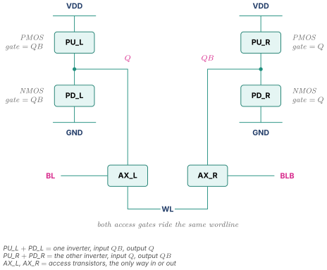
Six transistors. Four for the storage loop, two for access. Nothing else, and that minimalism is the point, because this structure is replicated tens of millions of times on a die and every wasted square nanometre is multiplied by that count.
2.3 Bistability is the same phenomenon as metastability
Plot the two inverter transfer curves on the same axes, one of them with its axes swapped so both live in the versus plane. The picture that results is called the butterfly curve.
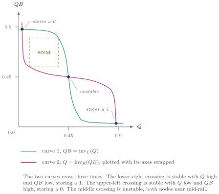
The middle crossing is the same object as the metastable point in Clocking Reset and Domain Crossing. A flip-flop is also built from cross-coupled inverters, and metastability is that flop being pushed onto the middle crossing, where the loop gain is not enough to resolve quickly and the node can linger for an unbounded time. Same structure, same three equilibria, opposite intent. In a flop the middle point is a hazard to be escaped. In an SRAM cell the two outer points are the product and the middle point is what you spend your design margin staying away from.
The static noise margin, written SNM, is how far you can push a stored node before it falls over the middle crossing into the other state. It is measured in millivolts, and every subsequent section of Part 4 is about protecting it.
2.4 SRAM against DRAM, and why the hierarchy has layers
A DRAM cell is one transistor and one capacitor. The capacitor holds charge, the transistor connects it to a bitline. That is it. Two devices instead of six.
The count understates the difference. Area is not proportional to transistor count, it is set by layout, and a DRAM process builds the capacitor vertically, either in a deep trench below the transistor or stacked above it, so the capacitor consumes almost no additional plan-view area. Measured in , where is the process feature size, a DRAM cell is around and a 6T SRAM cell is around to . That is a factor of twenty to twenty-five, not a factor of six. Exact comparison is slippery because DRAM and logic are built in different, specialized processes, but the order of magnitude is solid.
Now the consequences, and each one is a reason the memory hierarchy exists.
| Property | SRAM 6T | DRAM 1T1C | Consequence |
|---|---|---|---|
| devices per bit | 6 | 2 | area, and therefore cost per bit |
| area per bit | roughly | roughly | DRAM holds about 20x more bits in the same silicon |
| holds its value | indefinitely while powered | for milliseconds | DRAM needs periodic refresh |
| read | non-destructive, the loop restores itself | destructive, the charge is dumped onto the bitline | DRAM must write every read row back |
| access time | hundreds of picoseconds | tens of nanoseconds | SRAM can be in a CPU pipeline, DRAM cannot |
| process | ordinary logic process | specialized capacitor process | SRAM goes on the CPU die, DRAM does not |
| static power | leakage only | leakage plus refresh energy | large DRAM arrays burn power doing nothing useful |
Put a number on refresh so it stops being an abstraction. A DRAM bank must refresh every row within a retention window of about 64 ms. With 32768 rows in a bank and each refresh taking roughly 45 ns, the bank spends ms out of every 64 ms unavailable, which is about 2.3 percent of its time doing nothing but remembering. That fraction grows as capacity grows, and at high temperature the retention window halves roughly every 10 degrees Celsius, so it can reach the high single digits in a hot server part.
The destructive read is worth dwelling on because it has no SRAM analogue. Opening a DRAM row dumps the cell capacitors onto the bitlines, and the sense amplifiers then latch the values and drive them back into the cells. The row of sense amplifiers is therefore acting as a buffer holding the whole row, which is exactly what a DRAM row buffer is and why row hits are cheap and row misses expensive. An SRAM read leaves the cell holding its value because the cross-coupled loop is still powered and still fighting, which is why SRAM has no row buffer concept and no activate-precharge protocol.
So the layering falls out. SRAM is fast, non-destructive, buildable in a logic process, and expensive per bit, so you use a little of it very close to the pipeline. DRAM is slow, destructive, needs refresh, needs its own process, and is cheap per bit, so you use a lot of it far away. There is a middle option, eDRAM, which is DRAM built in a modified logic process and has been shipped as a large last-level cache in some server parts. It buys roughly three times the density of SRAM at the cost of refresh logic on the CPU die and a process adder, and it has largely lost ground to simply building more SRAM on cheaper nodes and to stacked memory.
03.Part 3, reading, and why sense amplifiers exist
3.1 Count the capacitance before designing anything
The single most important fact about an SRAM read is a ratio, and the ratio is not close.
The bitline is a vertical wire running the full height of the array. Every cell on it contributes the junction capacitance of its access transistor plus its share of the wire. Call that 0.6 fF per cell, an illustrative figure of the right order for a modern process. A subarray with 256 rows therefore presents
and once you add the wire itself and the sense amplifier's input, call it 150 fF as a round number.
The cell driving that bitline is two minimum-ish NMOS transistors in series, the access transistor and the pulldown, both deliberately made tiny because they are replicated tens of millions of times. Call the current they can deliver 30 uA.
Now use the delay expression from section 1.2 of Digital Logic and Timing, , and ask how long a full swing takes.
At 3 GHz that is 13.5 clock cycles, for one read, from a small array. That is catastrophic and it is why the naive picture of reading an SRAM is wrong.
Now ask how long a 100 mV swing takes.
Nine times faster, because appears linearly and you asked for one ninth of it. That is the entire trick. Do not wait for the bitline to swing. Wait only until you can tell which way it is going, then have a separate, fast, high-gain circuit finish the job. That circuit is the sense amplifier.
Notice what has just happened conceptually. The array has stopped being purely digital. Somewhere inside it there is a 100 mV analog signal being compared against a reference, and the correctness of your cache depends on that comparison. Everything strange about SRAM follows from this one design decision.
3.2 The four phases, drawn
A read proceeds in four phases. Each one exists for a reason, and skipping any one of them breaks something.
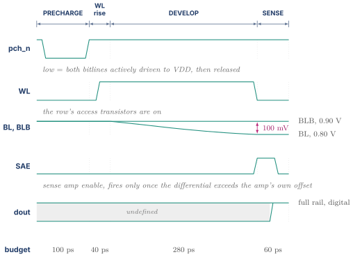
Precharge. Both bitlines are driven to the supply and then released to float. Both, not one, and equalized to each other, because the sense amplifier will compare them and any pre-existing imbalance is indistinguishable from signal. The precharge devices then turn off, leaving both lines floating high on their own capacitance. This is why a cache access has a precharge phase you can see in the timing, and why back-to-back accesses to the same subarray have a minimum spacing that has nothing to do with your pipeline.
Wordline rise. The row decoder drives one wordline high, turning on the access transistors of every cell in that row, all 288 or 512 or 1024 of them. Every one of those cells now begins fighting its own bitline pair. Note that you activated the whole row even though you probably only wanted 64 bits of it, and Part 5 explains why and what it costs in power.
Develop. Inside each cell, one internal node is low. Through its access transistor it drags the corresponding bitline down, slowly, at the rate the arithmetic above gave. The other bitline stays at the precharge level because the cell's other side is high and there is nothing to pull it anywhere. So a differential appears, and its sign encodes the bit. This is the phase whose duration is set by physics rather than by logic design.
Sense. Once the differential is comfortably larger than the sense amplifier's own input offset, the amplifier is enabled. It is itself a cross-coupled pair, the same structure as section 2.3, deliberately started at its unstable middle point and then tipped by the input differential. Positive feedback drives it hard to whichever rail the differential favors, in tens of picoseconds. Out comes a clean digital 0 or 1.
3.3 Why differential and not a threshold
An obvious simplification suggests itself. Precharge one bitline, let the cell pull it down, and compare it against a fixed reference voltage of say 0.85 V. Why keep two bitlines and compare them against each other?
Because almost everything that can go wrong moves both bitlines together and cancels in a difference. Supply noise from a neighboring block couples into both lines. Temperature shifts both precharge levels. Process variation in the precharge devices shifts both. Charge injection when the wordline rises couples into both. A single-ended comparison against a fixed reference sees all of that as signal. A differential comparison rejects all of it, because it is common mode, meaning identical on both inputs.
The remaining error is the sense amplifier's own input offset, meaning the differential voltage at which it is genuinely undecided, caused by mismatch between its own two halves. That offset is a random variable with a standard deviation of perhaps 20 to 30 mV in a modern process, and it is why you wait for 100 mV rather than 30 mV. You are buying sigmas of margin against your own amplifier being crooked, and Part 4's yield arithmetic applies here too.
Single-ended sensing does exist, and it is normal in register files and small arrays where the bitline is short, the read current is large, and the extra bitline track is more expensive than the lost noise immunity. That is a design point, not an error, and Part 5 comes back to it.
3.4 Two consequences that reach all the way up to your RTL
The array is an analog macro, so it is compiled and not synthesized. A sense amplifier's correctness depends on transistor matching, on the exact timing of its enable relative to the wordline, and on the precharge level. None of that is expressible in a standard cell library or checkable by static timing analysis in the ordinary way. If the sense enable fires 30 ps early, the amplifier tips on noise instead of signal and the array returns wrong data on some fraction of accesses at some corner of voltage and temperature. So the array is designed once by circuit designers, characterized exhaustively across corners, and delivered as a hard macro with guaranteed timing. Your synthesis tool is not permitted to have opinions about it. That is the direct answer to why you cannot just write a memory as a SystemVerilog array and let the tool figure it out, and it is a good short answer in an interview.
Develop time does not scale with logic speed, so cache latency in cycles has grown. Logic delay improved with every process node because transistors got faster. Bitline develop time is set by , and while improved, per cell fell only slowly and array capacities grew, and could not shrink below the sense amplifier's offset, which is set by mismatch and is stubborn. Meanwhile clock periods collapsed. So the same physical access time became more and more cycles.
| Era | Rough clock | Rough L1 access | L1 latency in cycles |
|---|---|---|---|
| mid 1990s | 100 MHz | around 8 ns | 1 |
| around 2000 | 1 GHz | around 2 ns | 2 |
| mid 2000s | 3 GHz | around 1.3 ns | 4 |
| modern high performance | 3 to 4 GHz | around 1.2 ns | 4 to 5 |
Those are order-of-magnitude public figures, not any particular part. The trend is the point. Absolute access time barely moved. Cycle count roughly quintupled. Every one of those extra cycles had to be absorbed by microarchitecture, which is where load-use speculation, speculative wakeup, and replay in Out of Order Execution came from, and why Cache Organization and Prefetching spends so much effort hiding latency that used to be free.
3.5 Where an access actually spends its time
Break a single-cycle-equivalent array access into its parts so the budget stops being mysterious. Take a 128-row subarray at 3 GHz, so the cycle is 333 ps.
| Step | Time | What sets it |
|---|---|---|
| address setup and predecode | 60 ps | ordinary logic |
| row decode and wordline driver | 90 ps | fanout of the wordline across the row, an RC problem |
| bitline develop to 100 mV | 280 ps | , the physics |
| sense amplifier resolve | 60 ps | positive feedback, fast |
| column mux and output drive | 70 ps | ordinary logic plus wire out of the macro |
| total | 560 ps | roughly 1.7 cycles at 3 GHz |
Read the middle row. Half the access time is one phenomenon, and it is the one you have the least control over. The only levers on it are shortening the bitline, which means more subarrays and more decode and more area, or increasing the cell current, which means bigger cells and less density, or reducing the required differential, which means a better sense amplifier and worse yield. That triangle is the whole of array design and it is why Part 5 looks the way it does.
There is a power consequence too, and it is large. Every access swings the full precharge charge back onto every bitline in the activated columns. Using from section 1.1 of Power Fundamentals and Clock Gating, restoring 150 fF through 100 mV on 288 bitline pairs costs pJ per access, because the precharge devices restore the swung line from the full rail. At one access per cycle at 3 GHz that is 23 mW for one small subarray. Bitline swing is the dominant dynamic power term in an array, which is why arrays are aggressively gated at the subarray level, why only the selected columns are precharged in many designs, and why the clock gating discipline of Power Fundamentals and Clock Gating applies with even more force to arrays than to logic.
04.Part 4, writing, the margin conflict, and the voltage floor
4.1 Writing means losing a fight on purpose
A read is designed so the cell barely disturbs the bitline. A write is the opposite. The write drivers grab both bitlines and drive them hard, one to ground and one to the supply, in the pattern you want stored. Then the wordline rises and the access transistors connect those driven bitlines to the internal nodes.
Now there is a fight. Suppose the cell holds V and you want to write a 0. The write driver is pulling BL to ground through a big, strong transistor. The cell's own PMOS pull-up PU_L is pulling to 0.9 V, because the cell still believes what it believes. Current flows from VDD through PU_L, through the access transistor AX_L, into the write driver, and down to ground. Whoever is stronger sets the voltage on .
The write succeeds if the driver can drag far enough below the switching threshold of the other inverter that inverter R flips high, at which point turns PU_L off and PD_L on, and the cell's own feedback finishes the job and slams to ground. So a write is not the driver forcing both nodes. It is the driver pushing one node just far enough that the loop's own positive feedback takes over and does the rest. The write margin is how much overkill you have in that push.
Two things follow immediately. Writing is faster than reading, because once the loop tips, the cell's own devices complete the transition at full speed rather than the driver having to charge everything. And writing is a contention operation, meaning it deliberately creates a temporary DC path from supply to ground inside the cell, which is why write energy per bit is higher than read energy per bit even though write is quicker.
4.2 The conflict, worked with transistor widths
Here is the tension, and it is the single best short answer to "what makes SRAM cell design hard."
For a read to be non-destructive, the access transistor must be weak compared with the cell's pulldown. During a read the bitline is at 0.9 V and the internal node holding 0 is connected to it through the access transistor. Charge flows in and lifts that node above ground. If the access transistor is strong and the pulldown weak, the node rises far enough to start turning on the other inverter, and the cell flips. That is a read disturb, and it is a silent data corruption caused by merely looking.
For a write to succeed, the access transistor must be strong compared with the cell's pull-up, because it has to drag the node holding 1 down against that pull-up.
The access transistor appears in both comparisons, in opposite directions. Two ratios name the two requirements.
Put widths on it, all at the same channel length. Take a pulldown of 200 nm, an access transistor of 130 nm, and a pull-up of 90 nm.
A cell ratio around 1.5 and a pull-up ratio well under 1 is a healthy cell. Now suppose writes are failing at low voltage and somebody suggests the obvious fix, widening the access transistor to 200 nm.
Writes got easier, exactly as intended. And the cell ratio fell to 1.00, which is well into read-disturb territory. You did not solve a problem, you moved it. Then somebody suggests widening the pulldown to 260 nm to restore to 1.3, and now the cell is larger in a structure replicated fifty million times, and you have traded away the density that was the reason to use 6T in the first place.
That is why the 6T cell has been essentially the same six transistors for thirty years with only the ratios being tuned. There is no clever rearrangement waiting to be found. There is a small, tightly constrained feasible region, and cell designers spend their careers inside it.
4.3 Why both margins collapse at low voltage, with the yield arithmetic
Now the part that most candidates state as a fact and cannot justify. Both margins shrink when the supply drops, and they shrink faster than linearly.
Two effects combine. First, the margins are fractions of the supply, so halving the supply roughly halves them in absolute millivolts before anything else happens. Second, and much worse, the thing eating those margins does not shrink. Transistor threshold voltages vary randomly from device to device because of random dopant fluctuation and line-edge roughness, and that variation has a standard deviation measured in millivolts that is a property of the device geometry, not of the supply. Call it mV, an illustrative but realistic figure for a small cell transistor.
So as the supply falls, the margin measured in millivolts falls while the noise measured in millivolts stays put. The margin measured in sigmas collapses.
Now ask how many sigmas you actually need, because this is where the number becomes shocking. Take an 8 MB last level cache.
Suppose you want 99.9 percent of manufactured parts to have zero marginal cells before any repair. Then the expected number of failing bits per part must be about 0.001, so the per-bit failure probability must satisfy
For a Gaussian, a one-sided tail probability of sits at about 6.6 standard deviations. So every one of those 67 million cells must have its margin exceed the mismatch distribution by 6.6 sigma, which at mV means roughly
Now put supply-dependent margins next to that requirement.
| Supply | Illustrative static noise margin | Margin in sigmas | Verdict for a 67 Mbit array |
|---|---|---|---|
| 1.00 V | 250 mV | 8.3 | comfortable |
| 0.90 V | 210 mV | 7.0 | fine |
| 0.80 V | 160 mV | 5.3 | marginal, needs repair and assists |
| 0.70 V | 110 mV | 3.7 | thousands of failing bits per part |
| 0.60 V | 70 mV | 2.3 | hopeless, roughly one percent of cells fail |
At 2.3 sigma the one-sided tail probability is about 0.01, so about 670,000 of your 67 million bits are broken. No redundancy scheme repairs that. The array simply does not work at 0.6 V.
That table is the answer to a question people give hand-wavy answers to. The array's minimum voltage is set by a six-sigma-plus requirement on a margin that is only a couple of hundred millivolts wide, against a mismatch distribution whose width does not scale. And because you need six sigma, the array Vmin is not where the typical cell fails. It is far above that, at the voltage where the worst cell out of sixty-seven million still works.
4.4 SRAM sets the minimum operating voltage of the chip
Logic is far more forgiving. A logic gate that is 20 percent slow than nominal is a timing problem you can fix by lowering the frequency. A cell whose noise margin has gone to zero is a functional failure at every frequency, exactly the asymmetry between setup and hold violations in section 5.6 of Digital Logic and Timing. And logic has only a few million critical instances, not sixty-seven million identical ones, so it needs far fewer sigmas.
The result is that a voltage domain containing an array can only drop to the array's Vmin, and that is almost always well above where the logic would still function. When DVFS Droop and Thermal talks about how low a DVFS operating point can go, this is what stops it. The lowest useful voltage of the whole chip is a bitcell property.
Three standard escapes exist and you should be able to name all three.
Dual rail. Give the arrays their own supply, held higher than the logic supply, so the logic can drop to 0.55 V while the arrays sit at 0.75 V. This works and is common. The cost is a second regulator or a second grid, level shifters at every boundary crossing per section 7.2 of Power Fundamentals and Clock Gating, and the area and complexity of two power grids in one block.
Assist circuits. Push the array's own Vmin down with extra circuitry, which is section 4.5.
A bigger, better cell. Offer an 8T or 10T cell with better margins at the cost of area, used selectively for the arrays that must run lowest.
4.5 Assist circuits
An assist is a circuit that temporarily and deliberately breaks the symmetry of the cell during exactly the operation that needs help, and gets out of the way afterwards. Each one buys margin somewhere and costs it somewhere else.
| Assist | What it physically does | Which margin it helps | What it costs |
|---|---|---|---|
| negative bitline write assist | boosts the write bitline below ground by 100 to 200 mV using a switched capacitor, so the access transistor sees more than the full supply across it | write margin | boost capacitor area, extra control timing, gate oxide stress on the access transistor |
| wordline underdrive | drives the wordline to less than the full supply during reads, weakening the access transistor | read stability | slower reads, and it makes writes harder so it must be read-only |
| wordline boost | drives the wordline above the supply during writes | write margin | oxide reliability, charge pump area |
| cell supply collapse | lowers the cell VDD of the selected column during a write, weakening the pull-up that is resisting | write margin | per-column supply switching, and it disturbs half-selected cells in the same column |
| read assist by supply raise | raises the cell VDD of the selected row during a read | read stability | needs a boosted rail, and it costs energy |
| dual rail array supply | runs the whole array at a higher fixed rail than the logic | both | second grid, level shifters, no DVFS on the array |
The phrase "half-selected cell" in that table deserves a definition because it is a favorite follow-up. When you write one word in a row, the wordline rises for the entire row, so every cell in that row has its access transistors on. The columns you are writing get driven bitlines. The columns you are not writing get bitlines left at the precharge level, which means those cells are being read whether you wanted to or not. Those are the half-selected cells, and they are exposed to the full read-disturb risk during a write. Any assist that weakens the cell to help the write, such as supply collapse, weakens the half-selected cells too, which is why cell supply collapse is applied per column and not per row.
05.Part 5, array organization and the price of ports
5.1 One monolithic array is unbuildable
Try to build a 1 Mbit array as a single 1024 by 1024 block and both dimensions fail at once.
Bitlines. 1024 cells on a bitline gives fF plus overhead, call it 620 fF. Develop to 100 mV takes
which is six cycles at 3 GHz for the develop phase alone.
Wordlines. A 1024-cell wordline is a long, thin, resistive wire with capacitance distributed along it. A distributed RC line has delay proportional to , and both and scale with length, so wordline delay scales with the square of the length. Quadrupling the width multiplies the wordline delay by sixteen.
Power. Activating a 1024-cell wordline turns on 1024 cells and swings 1024 bitline pairs, to deliver perhaps 64 bits. You paid for sixteen times the bits you used.
5.2 Banking and subarrays, compared with numbers
The fix is to break the array into many small pieces and only activate one. The vocabulary is worth getting right because interviewers use the words precisely.
A subarray is the smallest physical block with its own bitlines, its own sense amplifiers, and its own precharge. Splitting into subarrays shortens wires and saves power, and it is invisible to the outside world other than through timing.
A bank is an independently addressable unit with its own decoder and its own data path, so two accesses to different banks can proceed in the same cycle. Banking is architecturally visible, because two accesses to the same bank collide and one must wait. That is a bank conflict, and your arbiter has to handle it.
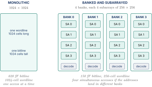
| Organization | Cells per bitline | Develop to 100 mV | Cells per wordline | Wordline RC, relative | Simultaneous accesses | |
|---|---|---|---|---|---|---|
| 1024 by 1024 monolithic | 1024 | 620 fF | 2.07 ns | 1024 | 16 | 1 |
| 4 subarrays of 256 rows | 256 | 150 fF | 0.50 ns | 1024 | 16 | 1 |
| 16 subarrays of 256 by 256 | 256 | 150 fF | 0.50 ns | 256 | 1 | 1 |
| 4 banks of 4 subarrays each | 256 | 150 fF | 0.50 ns | 256 | 1 | up to 4 |
Read the develop column. Going from a monolithic array to 256-row subarrays cut the dominant term by a factor of four, from 2.07 ns to 0.50 ns, which is the difference between a six-cycle array and a two-cycle array. That is the single biggest lever in array design and it costs decode logic, sense amplifier replication, and routing.
The costs are real and worth naming so the answer is not one-sided. Each subarray needs its own sense amplifiers, its own precharge devices, and its own local decode, and those repeat sixteen times. The global wires that carry addresses in and data out get longer because the array is now physically spread out. And the area overhead of a heavily subarrayed macro can be 30 to 50 percent above the raw bitcell area, which is why the ratio of bitcell area to total macro area, called array efficiency, is a headline number on a compiler datasheet and typically lands between 55 and 75 percent.
5.3 Aspect ratio and column multiplexing
Why not make every subarray extremely short and wide, so the bitlines are tiny? Because the wordline then becomes enormous and its RC delay goes as length squared. Why not extremely tall and narrow? Because the bitline capacitance goes back up. The compiler picks a shape that balances the two, and for typical processes a subarray lands somewhere between 128 and 512 rows and between 128 and 512 columns.
There is a second, purely physical constraint that decides the shape, and it surprises people. A sense amplifier is much wider than a bitcell. The cell is optimized to the absolute minimum pitch, perhaps 0.2 um wide. A sense amplifier is a matched differential pair with careful layout and it might need 1.6 um. So you physically cannot put one sense amplifier under every column. You put one under every eight columns and share it.
That sharing is the column multiplexer. An 8-to-1 column mux means each sense amplifier is switched between eight bitline pairs, and three address bits choose which.
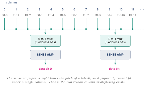
Column multiplexing has three knock-on effects you should be able to state.
It wastes read power, because the wordline activated all eight columns' cells and swung all eight bitline pairs to deliver one bit. Designs that care recover some of this by only precharging or only enabling the selected columns.
It makes narrow writes awkward, because the half-selected cells of section 4.5 are exactly the seven columns you did not want.
And it gives you bit interleaving for free, which turns out to be the single most important structural defense against multi-bit soft errors. Section 7.10 collects the payoff.
5.4 The address decomposition, drawn
Make it concrete with a 64 KB macro built as 4 subarrays of 256 rows by 512 columns with an 8-to-1 column mux, delivering 64 bits per access.
The macro holds words, so the address is 13 bits.
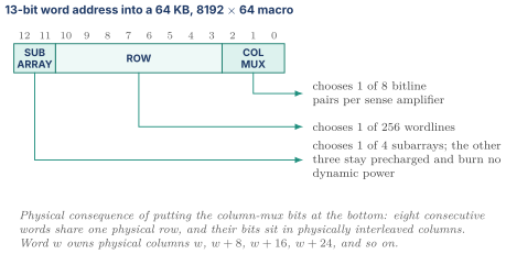
The placement of those three column-mux bits is a real design choice with real consequences. Putting them at the bottom of the address, as drawn, means consecutive words share a row, so a sequential burst of eight words hits one wordline and can be served from one activation, which is fast and low power. Putting them higher up spreads consecutive words across rows, which is worse for bursts but can be better for scattered access patterns. And whichever you choose determines which logical words are physically adjacent, which determines your soft-error multiplicity.
5.5 Multi-porting, and why area grows with the product
Now the most expensive thing you can ask an array for, and the place where interviewers separate people who have looked at a layout from people who have not.
A port is a way in or out. A single-port array can do one thing per cycle. A 2-read 1-write array can do three things per cycle. The naive expectation is that three ports cost three times one port. They cost far more, and the reason is geometric.
An SRAM bitcell is wire limited, not transistor limited. Its width is set by how many vertical wires must pass through it, meaning bitlines plus power. Its height is set by how many horizontal wires must pass through it, meaning wordlines plus ground straps. The transistors themselves fit in the space the wires leave.
Now count wires per port. A write port needs a differential bitline pair, two vertical tracks, plus one wordline, one horizontal track. A read port in a decoupled-read cell needs one single-ended bitline, one vertical track, plus one wordline, one horizontal track. Area is width times height, so it is a product of two sums, and that is where the quadratic comes from.
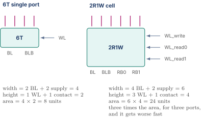
Tabulate it with a simple model where width equals 2 supply tracks plus one track per read bitline plus two per write bitline pair, and height equals 1 contact track plus one track per wordline.
| Configuration | Bitline tracks | Wordline tracks | Width | Height | Area units | Relative to 6T |
|---|---|---|---|---|---|---|
| 1RW, plain 6T | 2 | 1 | 4 | 2 | 8 | 1.0 |
| 1R 1W | 3 | 2 | 5 | 3 | 15 | 1.9 |
| 2R 1W | 4 | 3 | 6 | 4 | 24 | 3.0 |
| 4R 2W | 8 | 6 | 10 | 7 | 70 | 8.8 |
| 8R 4W | 16 | 12 | 18 | 13 | 234 | 29.3 |
Twelve ports costs twenty-nine times the area, not twelve times. The model is crude and real cells do better than a pure product because some tracks are shared, but the scaling is right and the message is right. Area grows roughly with the square of the port count, not linearly.
And area is not even the worst of it. More ports means longer wordlines and more bitlines hanging on each internal node, which means each port is individually slower. So a heavily ported array is simultaneously enormous and slow, which is precisely the wrong combination for a structure that sits in the execute loop.
5.6 The four ways to fake more ports
Because true multi-porting is so brutal, real designs almost never buy it directly above two or three ports. Four alternatives exist and a good answer names all four with their failure modes.
Banking with conflict handling. Build many independent single-port banks and hope simultaneous accesses land in different banks. Cheap in area, and it works well when the access pattern is spread out. It fails when two accesses collide, so you need arbitration, stall logic, and possibly replay. The cost is not area, it is a variable-latency array, which is much harder for a scheduler to plan around. This is why bank conflicts show up as a performance counter.
Double pumping, also called time multiplexing. Run the array at twice the core clock and perform two accesses per core cycle, presenting a virtual dual-port array. Costs almost no area. Fails because the array now has to close timing at half the cycle, and section 3.5 showed that the develop phase already eats most of a cycle. So double pumping works for small, short-bitline arrays and does not work for a large cache. It also creates a second clock domain inside the block with all the discipline of Clocking Reset and Domain Crossing.
Replication. Keep two or four identical copies of the data. Each copy is a cheap 1R1W array, reads go to whichever copy is free, and writes go to all copies. Area is times the single-copy area, which for the numbers above beats true porting badly. An 8R1W true array in the model is 10 bitline tracks by 9 wordline tracks, or 120 units, 15 times a 6T cell. Four replicated 2R1W arrays are units, 12 times, and every copy is individually fast because its wires are short. The cost is write bandwidth, since every write must reach every copy, and a coherence-like problem if writes and reads to different copies can be reordered. Clustered register files in the published literature, such as the Alpha 21264, took exactly this route.
Hierarchical or clustered organization. Split the consumers into clusters, give each cluster its own smaller array, and pay a penalty when a cluster needs a value that lives elsewhere. This is replication plus locality, and it converts an area problem into a scheduling problem.
| Approach | Area cost | Latency cost | New problem it creates |
|---|---|---|---|
| true multi-port | quadratic in ports | slower per port | none, it just costs too much |
| banking | small | none on a hit | bank conflicts, variable latency, arbitration |
| double pumping | almost none | halves the available cycle time | only works on small arrays, extra clock |
| replication | linear in copies | none, wires get shorter | write bandwidth to all copies |
| clustering | linear in clusters | inter-cluster transfer penalty | steering and scheduling complexity |
5.7 Register file array design
A register file is an SRAM array pushed to the opposite extreme from a cache, and topic 139 asks about it specifically. Get the contrast straight and it is memorable.
A physical register file in a wide out-of-order core might be 384 entries of 64 bits, with something like eight read ports and four write ports to feed and retire from multiple execution ports. Count the bits.
Three kilobytes. Now apply the porting multiplier from 5.5, where 8R4W came out at 29 times a plain 6T cell.
The register file holds three kilobytes and occupies more silicon than a 64 KB L1 cache. That number, worked out loud, is one of the most convincing things you can say about why register file design is its own discipline and why Execution Units spends so long on bypass networks and clustering. Every bypass path you build is a read port you did not have to buy.
The design differences follow from the extreme.
| Property | Cache data array | Register file |
|---|---|---|
| capacity | tens of KB to MB | a few KB |
| ports | 1 or 2 | 8 to 16 |
| latency | 2 to 5 cycles | 1 cycle, in the execute loop |
| bitcell | 6T, minimum area | 8T or larger, decoupled read |
| sensing | differential with sense amplifiers | often single ended, short local bitlines |
| built by | memory compiler | custom or semi-custom layout |
| ECC | parity or SECDED | parity at most, often nothing |
| what dominates area | bitcells | wires and ports |
The 8T cell with a decoupled read port deserves its own paragraph because it resolves the conflict of section 4.2 by construction. Add two transistors forming a small read buffer whose gate is the storage node and whose output drives a dedicated read bitline. Now a read never touches the storage node at all, it only senses it through a gate, so there is no read disturb and no read stability constraint. The access transistors then only have to satisfy the write requirement, which means they can be made strong and the cell can operate at a much lower voltage. The cost is the two extra transistors and the extra bitline track, which is why 8T is normal in register files and in low-voltage arrays and too expensive in a large cache.
The other register file specifics worth naming. Bitlines are kept extremely short by splitting the file into small local groups with local sense and a hierarchical global bitline, because a one-cycle read leaves no time for a long develop. Reads are frequently single ended because the bitline is short enough that noise immunity is not the binding constraint and a second track per port is unaffordable. And protection is minimal, because there is no spare cycle for a syndrome and the file is small enough that its contribution to the chip's soft error rate is modest. Where protection is required, the usual answer is parity plus a machine check rather than inline correction, or a radiation-hardened cell that stores the bit redundantly inside the cell itself.
06.Part 6, how arrays fail
Arrays are the most failure-prone structures on a die, and for two completely different reasons that need completely different fixes. Keeping them apart is half the battle.
6.1 Soft errors, from the physics up
A soft error is a stored bit changing value with nothing physically broken. Rewrite the location and it is fine. The cell is not damaged, it was simply knocked over.
The mechanism is ionizing radiation. Two sources matter on Earth.
Alpha particles from package materials. Trace radioactive contaminants in solder, molding compound, and interconnect metals, historically lead-210 and thorium and uranium daughters, emit alpha particles of about 5 MeV. Purified materials cut this enormously and it is largely a solved manufacturing problem, but it never goes to zero.
Cosmic ray secondaries. A primary cosmic ray hits the upper atmosphere and produces a shower. What reaches sea level in quantity is high-energy neutrons. A neutron is uncharged so it deposits no charge directly, but it can strike a silicon nucleus and shatter it, and the resulting charged fragments do the ionizing. The sea-level flux above 10 MeV is roughly 13 neutrons per square centimetre per hour at New York City in the standard JEDEC reference, rises by roughly a factor of three to four at Denver's altitude, and by a factor of a few hundred at commercial aircraft altitude. That is why avionics and high-altitude installations have visibly worse error rates and why the flux is a specified environmental parameter and not a constant of nature.
Now the arithmetic that shows why this is not a marginal effect. Take a 5 MeV alpha particle. It takes about 3.6 eV of deposited energy to create one electron-hole pair in silicon, so the total number of pairs along the track is
and the total charge liberated is
spread over a track of roughly 25 um, so about 9 fC per micron. Only the charge generated in and near the depletion region is collected quickly enough to matter, so the collected charge might be a few femtocoulombs to a few tens.
Compare that with what it takes to flip a cell. The critical charge is the charge that must be injected into a storage node to push it past the middle crossing of section 2.3 before the cell's own restoring current can fight it off. Approximate it as the node capacitance times the supply.
Perhaps one to two femtocoulombs once you account for the cell's restoring current during the strike. Against several femtocoulombs collected, it is not a close contest. The strike wins comfortably, and it has been winning by a larger margin every process generation, because falls with node capacitance and supply voltage while the physics of the particle does not change at all.
The industry unit is the FIT, one failure per device-hours. Per-bit raw SRAM soft error rates in public literature have run from around FIT per bit in planar processes down toward FIT per bit in FinFET generations, where the fin geometry presents a much smaller collection volume. Take FIT per bit as an illustrative planar figure and put it on an 8 MB cache.
One unprotected cache error every one and a half years per device sounds almost tolerable until you multiply by a fleet. Across 100 million shipped devices, the fleet rate is
Two silent data corruptions per second across the installed base, forever. That is the number that makes ECC non-negotiable, and it is worth being able to produce on demand because it converts an abstract reliability argument into a product argument. Even at the FinFET figure of FIT per bit it is one every five seconds.
6.2 What shrinking cells does, in both directions
The intuitive answer is that smaller cells are more vulnerable, and that is half right in a way worth understanding precisely, because the full picture explains the single most important structural defense in Part 7.
Smaller is worse, because falls. Node capacitance shrinks with the device and supply voltage shrinks with the process, and is roughly their product, so it falls on both counts. A strike that would once have been shrugged off now flips the cell.
Smaller is better, because the cross section falls. A cell that occupies a quarter of the area presents a quarter of the target to an incoming particle. Fewer strikes land on it at all.
Those two effects have largely cancelled, and per-bit soft error rates have been roughly flat to slowly declining for several generations, with FinFET giving a real step improvement because the conducting channel is a thin fin sitting above the bulk rather than a large junction embedded in it, so most of the liberated charge never gets collected.
But two things did get worse and both matter.
Per-chip rates rose, because bit counts exploded. Flat per-bit multiplied by ten times the bits is ten times the failures.
Error multiplicity rose, and this is the dangerous one. As cells shrank, a single particle track that once covered one cell now covers three or four adjacent cells, and the charge it deposits is shared among them. The result is a multi-cell upset, or MCU, where one event flips several physically adjacent bits at once.
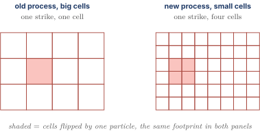
That single change breaks the standard defense, because the standard code corrects one error per protected word and merely detects two. If those four adjacent cells happen to be four bits of the same logical word, the code sees a four-bit error, which it neither corrects nor is guaranteed to detect, and it may confidently miscorrect and hand you data that is now worse than what it received. Section 7.10 is the fix and it is purely a layout decision, which is why the address decomposition of section 5.4 mattered.
6.3 Hard errors, redundancy, and repair
A hard error is a permanently broken cell, from a manufacturing defect, a stuck contact, a shorted bitline, or wearout mechanisms over the product's life. Rewriting does not help. This is a yield problem, not a reliability problem, and it is fixed by physical redundancy rather than by codes.
Work the yield to see why redundancy is universal. Take a per-bit defect probability of , an illustrative figure. A 512 Kbit macro then has an expected defect count of
so 99.9 percent of individual macros are perfect. Fine. But a chip contains many macros. With 200 of them,
Nineteen percent of parts thrown away because of single broken bits in arrays. That is an unshippable yield loss and it is why every serious array ships with spares.
Now add two spare columns per macro, so a macro only fails if it has more than two defects. For a Poisson with the probability of three or more is about , and across 200 macros that is . Yield goes from 81 percent to essentially 100 percent for a few percent of extra array area. That is one of the best returns on area anywhere in chip design, and it is why redundancy is not optional.
The mechanism is worth naming precisely because it is a DFT conversation as much as a design one. Memory BIST is a small state machine attached to the array that writes and reads known patterns at speed and reports failing addresses. Built-in redundancy analysis takes the failing address list and computes a repair solution, meaning which spare row or column should replace which failing one. Built-in self repair then programs that solution permanently, historically by blowing laser or electrical fuses, so the repair is applied automatically at every subsequent power-up by remapping the decoder. All three run at wafer test, and a modern part carries a fuse array whose only job is holding repair solutions. DFT and Silicon Debug carries the test-side treatment.
Two limits are worth knowing. Redundancy repairs a small number of localized defects and cannot help with a systematically weak array, and the spare granularity matters, since a spare column repairs one bad bit in every row of a subarray while a spare row repairs a whole bad wordline, so you generally want both.
6.4 The three outcomes, and why one of them is the enemy
Every error event ends in one of exactly three states, and the industry vocabulary for them is used constantly.
| Outcome | Abbreviation | What happened | How bad |
|---|---|---|---|
| corrected error | CE | the code found and fixed it, the machine continued | logged, harmless, but a rising rate predicts a failing part |
| detected uncorrectable error | DUE | the code knew it was wrong and could not fix it | the machine must stop, poison the data, or take a machine check, so it is a crash rather than a lie |
| silent data corruption | SDC | the wrong value was delivered and nobody knew | catastrophic |
SDC is the enemy. A crash is recoverable, annoying, and diagnosable. A wrong answer that propagates into a filesystem, a financial calculation, or a training run is none of those. So the entire design of Part 7 is organized around converting potential SDCs into CEs where possible and into DUEs where not, and the value of a code is measured much more by how few SDCs it leaves than by how many errors it corrects.
That framing also explains a design decision that otherwise looks lazy. Some structures get no protection at all, and that is correct rather than negligent, because an error in them cannot produce an SDC. Section 7.8 collects those cases.
07.Part 7, error correcting codes from the ground up
This is the part to be strongest on, and it is best built from a tiny concrete example rather than from definitions.
7.1 Redundancy, distance, and what a code actually is
Send one bit down a wire. It arrives as a 0. Is it correct?
You cannot possibly tell, and the reason is not subtle. There are two possible messages and two possible received values, and every received value is a legal message. There is no observation that distinguishes "the sender sent 0" from "the sender sent 1 and it flipped." Detection is impossible in principle, not merely hard.
So send it three times. The sender is only allowed to transmit or . Those two are the codewords. The other six three-bit strings are illegal. Now if you receive , you know something went wrong, because is not a legal transmission. And you can do better than know. differs from in one position and from in two, so if you believe single errors are much more likely than double errors, is the better bet. Take the majority vote and you have corrected the error.
Draw all eight three-bit strings as the corners of a cube.
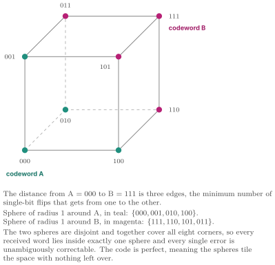
Only now do the definitions mean something. The Hamming distance between two binary strings is the number of positions where they differ. The minimum distance of a code is the smallest Hamming distance between any two of its codewords. And the two facts that govern everything follow directly from the picture.
Detection needs because flips must never be able to land you exactly on another codeword. Correction needs because the spheres of radius around each codeword must not overlap, and two spheres of radius are disjoint only if their centres are more than apart.
The repetition code has , so it corrects or detects , and notice the "or." You choose. If you use the code to correct single errors, then a double error like lands in B's sphere and you will confidently "correct" it to , producing three wrong bits from two. If instead you decline to correct and only report legality, you catch every double error. A code's distance is a fixed budget and correction and detection spend from the same budget. That single sentence explains the entire structure of SECDED in section 7.4, and it is the conceptual crux of this Part.
The price here is brutal. Three bits sent for one bit of data is a code rate of and an overhead of 200 percent. Nobody pays that for memory. The rest of Part 7 is about getting the same distance far more cheaply, and the way you do it is by protecting many data bits together instead of one at a time.
7.2 Parity, the one-bit code
The cheapest possible code adds a single bit chosen so the total number of ones is even. That is even parity, and the parity bit is simply the XOR of all the data bits.
Take the byte . It has five ones, which is odd, so the parity bit is 1 and the transmitted nine bits are with six ones total. On receipt, XOR all nine bits. If the answer is 0 the word is consistent, if it is 1 something flipped.
Flip bit 3 in transit, giving with seven ones. XOR of all nine is 1. Detected.
Now flip bits 3 and 5, giving with eight ones. XOR of all nine is 0. Not detected. The word looks perfectly healthy and you will use it.
That behaviour is exactly what the distance rule predicts. Any two parity-protected words differ in at least two positions, one data bit plus the parity bit that follows it, so . From you get , meaning detect one error. From you get , meaning correct nothing. Parity detects any odd number of errors and is blind to any even number, and corrects nothing at all.
The overhead is negligible. One bit on 64 is 1.6 percent. The hardware is one XOR tree. So the question is not whether parity is cheap, it is when detection without correction is enough.
The rule is short and it is the answer to a very common interview question. Parity suffices exactly when a known-good copy of the data exists somewhere else and you can afford to go get it.
The canonical case is an L1 instruction cache. Instructions are read-only from the cache's point of view, so every line in it is clean, which means an identical copy exists in L2 or memory. Protect it with parity per some granule. On a parity error, do not correct, do not panic, just invalidate the line, treat the access as a miss, and refetch. The instruction stream is unaffected apart from a few tens of cycles. Correction machinery would buy nothing over a mechanism the pipeline already has, because refill on a miss is the front end's ordinary behaviour per Front End and Branch Prediction.
The same argument covers clean lines in a data cache, a TLB whose entries can be re-walked from the page tables per Virtual Memory and Memory Ordering, and any structure that is a cached copy of something authoritative elsewhere.
Where parity fails is the moment the array holds the only copy. That is section 7.4's argument for write-back caches, and it is the reason SECDED exists.
7.3 Hamming's construction, derived rather than quoted
Repetition is too expensive because it protects one bit at a time. The insight that fixes it is to protect data bits together with check bits and to make each check bit answer a different question about the whole word.
Before building anything, count what the check bits have to accomplish. After receiving a word, you must be able to distinguish these outcomes:
- no error at all, which is one outcome
- an error in any one of the transmitted positions, which is outcomes
That is distinct answers you need to produce. The check bits, recomputed and compared, give you bits of information, which can name at most things. So
That inequality is not a formula to memorize, it is a counting argument, and being able to derive it in ten seconds at a whiteboard is worth more than knowing the answer. It says nothing more than that yes-or-no questions must be enough to name every possible outcome.
Solve it for . Try , giving , false. Try , giving , true and exactly tight. So four data bits need three check bits, for a seven-bit codeword. That is the (7,4) Hamming code, and its tightness makes it a perfect code in the sphere-packing sense of section 7.1.
Now the construction, which is where Hamming's actual cleverness lives. Number the seven positions 1 through 7. Put the check bits at the positions that are powers of two, so positions 1, 2, and 4, and put the data bits everywhere else, so positions 3, 5, 6, and 7. Then define check bit at position to cover exactly those positions whose binary representation has the bit for set.
| position: 1 2 3 4 5 6 7 | |
| holds: p1 p2 d1 p4 d2 d3 d4 | |
| position in | |
| binary: 001 010 011 100 101 110 111 | |
| p1 covers every position whose bit0 is 1 -> 1, 3, 5, 7 | |
| p2 covers every position whose bit1 is 1 -> 2, 3, 6, 7 | |
| p4 covers every position whose bit2 is 1 -> 4, 5, 6, 7 | |
| Written as a parity check matrix H, one column per position: | |
| 1 2 3 4 5 6 7 | |
| row c1 [ 1 0 1 0 1 0 1 ] | |
| row c2 [ 0 1 1 0 0 1 1 ] | |
| row c4 [ 0 0 0 1 1 1 1 ] | |
| Column j is simply the binary number j. That is the entire trick. |
Work an example. Take data , placed at positions 3, 5, 6, 7.
covers positions 1, 3, 5, 7, which hold . For even parity, . covers positions 2, 3, 6, 7, which hold . So . covers positions 4, 5, 6, 7, which hold . So .
The transmitted codeword, positions 1 through 7, is .
Now flip position 6. The received word is . Recompute each check.
XOR of positions 1, 3, 5, 7 . XOR of positions 2, 3, 6, 7 . XOR of positions 4, 5, 6, 7 .
Read them as a binary number with as the most significant bit. That is . The syndrome is the number of the failing position, directly, with no lookup table. Flip position 6 back and the word is repaired.
That is why the check bits sit at powers of two. Position 6 is in binary, meaning it is covered by and and not by , so exactly those two checks fail, and the pattern of failing checks spells the position. Any single error produces the column of H corresponding to its position, and since every column is a distinct nonzero binary number, every single error produces a distinct nonzero syndrome. That is the whole proof of single-error correction, in one sentence.
Two structural facts follow that get asked as follow-ups. The all-zero syndrome means no error, which is why the zero column is excluded and why no position is left uncovered. And a check bit error is also correctable, because position 2 is covered only by , so its syndrome is , pointing at itself.
7.4 Why plain Hamming is dangerous, and the extension to SECDED
Plain Hamming has , so by the budget rule of 7.1 it can correct one error or detect two, not both. Used as a corrector it does something actively harmful on a double error, and seeing it happen once makes the point permanently.
Take the same codeword and flip two bits, positions 3 and 5. The received word is .
positions 1, 3, 5, 7 . positions 2, 3, 6, 7 . positions 4, 5, 6, 7 .
Syndrome . The decoder concludes that position 6 is wrong and flips it. Positions 3, 5, and 6 are now all wrong. Two errors went in and three came out, with no indication that anything unusual happened. That is a silent data corruption manufactured by the error correction hardware.
The mechanism is one line of algebra. The syndrome is linear, so two errors produce the XOR of their two columns, and
The XOR of two distinct nonzero columns is another nonzero value, and in a perfect code every nonzero value is some column, so a double error always aliases onto a single-error pattern. There is no exception and no clever decoder that escapes it. You need more distance.
The fix is small. Add one more check bit that is the overall parity of the entire codeword, all seven positions plus itself. That lifts the minimum distance from 3 to 4. Now the two failures separate.
Compute it for the running example. The seven-bit codeword has four ones, so the overall parity bit , and the eight-bit transmitted word is followed by .
A single error flips one bit, changing the total parity, so the overall check comes out 1, and the syndrome is nonzero. A double error flips two bits, leaving the total parity unchanged, so the overall check comes out 0, and the syndrome is still nonzero.
Those two cases are now distinguishable, and that is the entire content of SECDED.
| Overall parity check | Syndrome | Verdict | Action |
|---|---|---|---|
| 0 | zero | clean | use the data |
| 1 | nonzero | single error, at the position the syndrome names | flip that bit, use the data, log a CE |
| 1 | zero | the overall parity bit itself flipped | data is fine, log a CE |
| 0 | nonzero | double error | uncorrectable, do not use, raise a DUE |
SECDED stands for single error correct, double error detect, and it is an extended Hamming code, the word extended meaning exactly that added overall parity bit. Note that the two capabilities coexist only because funds both, one error of correction radius plus one more of detection.
State the limit honestly, because a good interviewer will push on it. SECDED gives you nothing beyond two errors. A triple error flips an odd number of bits, so it produces odd overall parity and a nonzero syndrome, which is indistinguishable from a single error. The decoder will confidently correct some innocent fourth position and hand you four wrong bits. Three-bit errors inside one protected word are silent data corruptions, full stop. Section 7.10 exists because multi-cell upsets threaten to make three-bit errors common, and section 7.9 exists because accumulation over time threatens to make two-bit errors common.
7.5 Sizing it for 64 bits, the number to know
Now solve for .
Try . Then and . Is ? No. Try . Then and . Is ? Yes, comfortably.
So seven check bits give single error correction on 64 data bits, for a 71-bit codeword. Add the overall parity bit for double error detection and you get
That is the standard configuration in caches and in DRAM DIMMs, it is why an ECC DIMM has nine chips per rank instead of eight, and it is the single number most likely to be asked directly.
Notice from giving 128 possible syndromes against only 72 needed positions that the code is far from tight at . That slack is what lets you choose a better H matrix in section 7.6, and it is also why the overhead keeps falling as words get wider.
| Data bits | Check bits for SEC | Plus DED | Total | Overhead |
|---|---|---|---|---|
| 8 | 4 | 5 | 13 | 62.5 percent |
| 16 | 5 | 6 | 22 | 37.5 percent |
| 32 | 6 | 7 | 39 | 21.9 percent |
| 64 | 7 | 8 | 72 | 12.5 percent |
| 128 | 8 | 9 | 137 | 7.0 percent |
| 256 | 9 | 10 | 266 | 3.9 percent |
| 512 | 10 | 11 | 523 | 2.1 percent |
The overhead falls roughly as , so wider is dramatically cheaper. Which raises the obvious question and its counterintuitive answer.
If wider is cheaper, why does anybody use 64-bit granules instead of 512-bit granules? Three reasons, and they are all more important than the area.
Partial writes force a read-modify-write. If the ECC granule is 512 bits and a store writes 8 bits, the check bits depend on all 512, so you must read the other 504 bits out of the array, merge your 8 bits in, recompute the code, and write all 523 bits back. That is an extra array access on the store path, plus a structural hazard against any concurrent access to that subarray, plus a read-after-write ordering problem in your store pipeline per Load Store and Memory Ordering. With a 64-bit granule a 64-bit store needs no read at all, and a byte store still needs one but touches far less.
Correction strength per bit falls. One correctable error per 512 bits is eight times weaker than one per 64 bits at the same raw per-bit upset rate, so the residual double-error rate is eight times higher for the same scrub interval.
Latency rises. A wider XOR tree is a deeper XOR tree, and section 7.6 shows that the tree is already most of a cycle.
So the granule is a genuine design point, not a formality. The usual resolution in a cache is a 32-bit or 64-bit ECC granule on the data array, sometimes with byte-level parity layered underneath so that byte stores can be validated without a full read-modify-write. Being able to lay out that tradeoff is exactly the kind of answer a cache role is listening for.
7.6 Encoding hardware, and the H matrix that real designs use
The encoder is pure XOR. Each check bit is the XOR of the data bits its row of H selects, so the whole encoder is a set of XOR trees running in parallel over the data word.
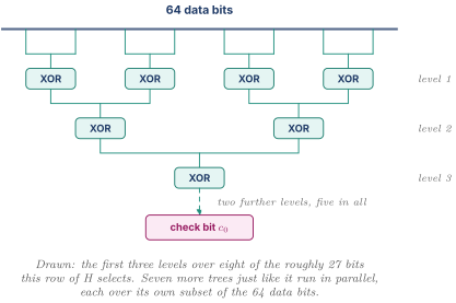
Count the depth. In the standard Hsiao construction, which is what real designs use, the 72 columns of H are chosen to all have odd weight, meaning an odd number of ones, and to be distinct. The number of odd-weight 8-bit vectors is , comfortably more than the 72 columns needed. The usual choice takes 8 columns of weight 1, which are the check bits themselves, 56 columns of weight 3, which is all of , and 8 columns of weight 5. Total ones in H is
spread over 8 rows, so about 27 ones per row. Each check bit is therefore an XOR of roughly 27 bits, and a balanced binary XOR tree over 27 inputs has depth . At 30 ps per XOR2 gate that is 150 ps of encode delay. At 3 GHz the cycle is 333 ps, so the encoder alone eats 45 percent of a cycle.
Gate count is small. A row with ones needs two-input XORs, so the whole encoder is XOR gates. Two hundred gates to protect 64 bits is nothing. Area is not the problem with ECC. Latency is. That is the sentence to lead with when asked what ECC costs.
Two things about Hsiao's construction are worth knowing because they are exactly the kind of hardware-aware code design a PPA discussion rewards.
Odd column weight replaces the separate overall parity bit. Any single error produces a column of H, which has odd weight, so the syndrome has an odd number of ones. Any double error produces the XOR of two odd-weight columns, which has even weight and is nonzero. So you distinguish single from double by counting the parity of the syndrome itself, with no extra bit and no extra tree. The DED comes free out of the structure.
Minimizing and balancing the ones in H is a direct PPA optimization. Total ones sets the gate count. The maximum ones in any single row sets the worst tree depth and therefore the critical path. Hsiao's construction minimizes the total and balances the rows, which is why it beat the naive positional Hamming layout of section 7.3 in every implementation. The positional layout is for teaching. The Hsiao layout is for silicon.
7.7 Decoding, and keeping correction off the critical read path
Decoding is the expensive direction and its cost is why ECC is a microarchitecture problem rather than a coding problem.
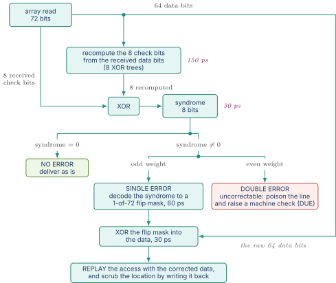
Add the inline path. Syndrome generation is 150 ps plus 30 ps of XOR, the one-hot decode of 8 syndrome bits to a 72-bit flip mask is about 60 ps, and the correction XOR is another 30 ps, for roughly 270 ps of pure ECC latency. Against a 333 ps cycle that is 81 percent of a cycle, on top of the array's own 560 ps from section 3.5, and all of it sits between the array and the consumer.
You cannot afford that inline. So the standard structure is check in parallel with use.
Deliver the raw data to the consumer the moment the array produces it, exactly as if there were no ECC at all. In parallel, run the syndrome computation. One or two cycles later the syndrome resolves. If it is zero, which it is essentially always, nothing happens and the ECC cost was zero. If it is nonzero, raise an error signal that squashes everything downstream of that load and replays it with the corrected value.
| Cycle | Array | ECC logic | Consumer |
|---|---|---|---|
| 0 | address, decode, wordline | idle | issues the load |
| 1 | develop, sense | idle | waiting |
| 2 | column mux, drive out 72 bits | syndrome trees start | receives raw 64 bits, uses them speculatively |
| 3 | idle | syndrome resolves, error flag asserted or not | dependent ops already executing |
| 4 | re-read or correct in place | flip mask applied | squash and replay if the flag fired, otherwise nothing happened |
Notice what this design requires. The machine must already be able to squash and replay. An out-of-order core has that machinery for branch misprediction per Out of Order Execution and for load speculation per Load Store and Memory Ordering, so ECC recovery is nearly free, being just one more reason to fire an existing recovery path. A simple in-order machine has no such mechanism and either has to build one, stall until the syndrome resolves, or accept the inline latency. This is why ECC is cheap in a big out-of-order core and comparatively expensive in a small in-order one, and it is a genuinely good thing to say in a cache interview because it connects the code to the pipeline.
The write path is easier. The encoder's 150 ps sits on the store path, and stores are almost never latency critical because the store queue is already buffering them, so an extra pipeline stage for encode costs nothing that anybody notices.
One more implementation note that gets asked. On a corrected error, you should not merely fix the value in flight, you should also write the corrected value back into the array, because the upset cell is still holding the wrong bit and will fail again on every subsequent read, and worse, will eventually be joined by a second upset in the same word. That write-back on a correction is called demand scrubbing, and it leads directly to the next section.
7.8 Where the code lives, and matching protection to consequence
Different structures get different protection, and the choices are not arbitrary. There is one organizing principle and everything follows from it.
Protection strength is set by two things, whether a known-good copy exists elsewhere, and what a silent corruption of this structure would cost.
| Structure | Typical protection | Why |
|---|---|---|
| branch predictor tables, BTB | none | a wrong prediction is already an expected event, so an upset costs performance and cannot cause a wrong answer |
| prefetcher state, replacement state | none | pure hints, an error costs a few cycles at most |
| L1 instruction cache data | parity | always clean, a detected error becomes an invalidate and a refetch from L2 |
| L1 instruction cache tags | parity | a parity error is treated as a miss, which is always safe for a clean array |
| L1 data cache, write-through | parity | the write-through means L2 already has the data, so detect and refill |
| L1 data cache, write-back | SECDED | the array holds the only copy of a dirty line, so detection without correction is a data loss |
| L1 data cache tags, write-back | parity plus care, or ECC | losing a dirty line's identity is a correctness problem, so many designs duplicate tags or protect them harder |
| TLB entries | parity | rebuildable from the page tables by re-walking |
| L2 and L3 data | SECDED, sometimes stronger | large, long residency, and often the only copy |
| DRAM | SECDED, or symbol codes for chipkill | huge capacity and whole-device failure modes |
| register file | parity or nothing | one-cycle latency leaves no room, and the structure is small |
| store queue and other holding buffers | parity plus replay, or ECC | they hold the only copy of in-flight data, but only briefly |
Look at the top row and the bottom row together, because the contrast is the whole lesson. A branch predictor gets zero protection and that is the correct engineering decision, not laziness, because a corrupted prediction produces a mispredict, and the machine recovers from mispredicts thousands of times a second by design. A write-back L1 data array gets full correction because a corrupted dirty line becomes a wrong value in memory that nothing will ever notice. Same silicon, same particle, same upset rate, opposite decisions, driven entirely by consequence.
The write-back argument deserves stating in its own sentence because it is a common question. A write-back cache must correct rather than merely detect, because a dirty line is the only copy of that data anywhere in the machine, so a detected uncorrectable error in it is unrecoverable data loss rather than a refetch. A write-through cache can get away with parity, and that is one of the real arguments for write-through L1 designs alongside the coherence simplifications discussed in Cache Coherence Protocols.
The tag array case is subtler than most candidates expect, so it is worth having ready. A single-bit error in a tag has two possible effects. It can cause a false miss, where the tag no longer matches an address that is in fact present, and that is harmless for a clean line since you simply refill. Or it can cause a false hit, where a corrupted tag accidentally matches an address that is not present, and that returns completely unrelated data as if it were correct, which is an SDC of the worst kind. Parity catches the single-bit error before either can be acted on, which is why parity on tags is usually enough. But for a dirty line, discovering a bad tag means you no longer know where to write the data back, so it is not recoverable by invalidation. Designs handle that by protecting write-back tags more strongly, by duplicating the tag array, or by forcing the affected line's data through the machine check path.
7.9 Scrubbing, and the accumulation failure
SECDED corrects one error in a word and detects two. Errors do not arrive all at once, they accumulate slowly over the life of the part, and the failure it prevents is a second upset landing in a word that already carries an uncorrected first one.
Put numbers on it. Take a 32 MB last level cache at the illustrative FIT per bit.
Over a five-year life of 43,800 hours, the expected number of upsets in that array is
The array holds million 64-bit ECC words. If those 11.8 upsets land uniformly at random and nothing ever cleans them up, the expected number of pairs landing in the same word is a birthday calculation.
per part over five years. Small. Now multiply by a fleet of 100 million devices and it becomes 1,660 uncorrectable errors across the installed base, every one of them a machine check or a crash on a part that was never physically defective.
The fix is scrubbing, a background process that walks the array, reads each word, and if the syndrome is nonzero and correctable, writes the corrected value back. Errors are removed before a second one can join them.
Redo the arithmetic with a 24-hour scrub interval. Within one window the expected upset count is , and the collision expectation for that window is . Multiply by the 1,825 windows in five years and the lifetime expectation is per part, so about 0.9 events across the entire 100-million fleet. From 1,660 to under 1.
The scaling law is worth extracting because it is the answer to "how often should you scrub." Per word with upset rate and scrub interval , the probability of two upsets in one window is about , and there are windows per unit time, so the uncorrectable rate is
Linear in the scrub interval and quadratic in the upset rate. Halving the scrub period halves the double-error rate. Doubling the environmental upset rate, by flying the machine at altitude for instance, quadruples it. That asymmetry is why aggressive scrubbing is standard in high-altitude and high-reliability deployments.
The cost is essentially zero, which is the pleasant part. Walking 4.19 million words in 24 hours is
At 3 GHz that is one array access every 62 million cycles. It steals an idle cycle, it never contends with real traffic in practice, and its power is unmeasurable.
Two variants exist and both names get used. Patrol scrubbing is the background walk just described, driven by a slow address counter in a state machine. Demand scrubbing is the write-back-on-correction from the end of section 7.7, which cleans up any location that happens to be read. Real designs do both, because demand scrubbing covers hot data for free and patrol scrubbing covers cold data that might not be read for months. Cold data is precisely where accumulation happens, so patrol scrubbing is the one that matters for the arithmetic above.
One implementation caution. A scrub is a read-modify-write inside the array, and it must not look like a coherence transaction, must not disturb replacement state, and must not evict anything. Getting that wrong turns a reliability feature into a performance bug, and it is a real integration detail rather than a theoretical one.
7.10 Interleaving, and the multi-cell upset
Section 6.2 established that a single modern particle strike can flip several physically adjacent cells. Section 7.4 established that SECDED handles one error per word, detects two, and silently miscorrects three. Put those together and there is a serious problem, and the fix is beautiful because it costs nothing.
If a logical 72-bit word occupies 72 physically adjacent columns, then a strike covering four adjacent cells puts four errors in one word. That is beyond SECDED entirely, and being an even number it may well produce an even-weight syndrome that looks like an ordinary detectable double error, or it may alias to a single-error pattern and get miscorrected. Either way the machine is in trouble.
The fix is to lay the array out so that physically adjacent columns belong to different logical words. This is bit interleaving, and the interleave degree is how many different words are spread across each contiguous run of columns.
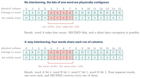
Interleaving does not reduce the number of upset cells by a single bit. It changes their distribution, and distribution is exactly what the code cares about. One four-bit event that SECDED cannot handle becomes four one-bit events that SECDED handles perfectly. That is the whole idea and it is one of the most elegant things in the field.
Now recall section 5.3. An 8-to-1 column multiplexer means eight logical words already share every physical row and their bits already alternate across the columns. The column mux ratio you chose for sense amplifier pitch reasons is exactly the interleave degree you get for free. The two constraints happen to point the same way, which is why interleaving is nearly universal and rarely costs anything explicit.
The costs, where there are any, are worth naming. Interleaving constrains the column mux ratio to be at least the interleave degree you want, which constrains the aspect ratio, which feeds back into the timing of section 5.2. It makes narrow writes messier because the bits you want to change are scattered. And it complicates repair, because a single bad column now affects one bit in each of several words rather than several bits in one, which is actually the friendly direction since single-bit-per-word failures are exactly what the code handles.
The interleave degree needed is set by measurement, not by theory. Accelerated beam testing produces an MCU size distribution, and you choose an interleave degree that covers the tail of it, commonly 4 or 8 in modern arrays.
7.11 Stronger codes, and where each one lives
SECDED is one point in a large design space, and knowing the shape of the space is what distinguishes someone who has studied coding from someone who has memorized "seventy-two slash sixty-four."
DECTED, double error correct triple error detect, comes from a BCH code with . For you need check bits with , since , plus one for the extension, so 79 bits for 64, or 23 percent overhead. The decoder is no longer a lookup, because with two errors the syndrome no longer names a position and you must actually solve for the error locator polynomial, which means finite field arithmetic and multiple cycles. It appears in high-reliability last-level caches and in some server memory, and its cost is latency rather than bits.
Symbol codes are the important conceptual jump. Instead of treating the word as independent bits, treat it as symbols of bits each, drawn from the finite field . A Reed-Solomon code over with parity symbols corrects symbol errors, and here is the crucial property. A symbol counts as one error no matter how many of its bits are wrong. A burst that destroys an entire symbol is one symbol error, not bit errors.
That property is exactly what chipkill needs. A DRAM rank is built from many separate memory devices, and a whole device can fail, taking out its four or eight bits of every transferred word simultaneously. To SECDED that is a four- or eight-bit error and it is hopeless. Arrange the code so that the four bits contributed by one x4 device are exactly one symbol of , and a whole dead device becomes a single symbol error, correctable by a code with two parity symbols. The failure of an entire chip is corrected transparently and the system keeps running, which is where the name comes from. If you additionally know which device failed, that is an erasure rather than an error, and erasures cost half as much, one parity symbol each, because you only need to solve for the value and not for the location.
BCH and LDPC for flash. NAND flash lives in a completely different error regime, and the comparison sharpens what SECDED actually is. A modern TLC or QLC NAND cell stores 8 or 16 distinguishable charge levels in a shrinking window, so raw bit error rates run from around up toward near end of life, against an SRAM raw bit error rate that is effectively zero on any timescale short of a year. Take a 4 KB codeword at a raw BER of .
Three hundred and twenty-eight errors that must all be corrected, against SECDED's one. And the overhead used to do it is roughly 7 to 12 percent, which is less than SECDED's 12.5 percent. That comparison is the single most useful thing to have ready about coding theory, because it demolishes the intuition that overhead determines strength. Overhead does not determine correction capability. Code structure and codeword length do. A long codeword amortizes redundancy across many more bits, and an iterative soft-decision decoder like LDPC extracts far more from the same parity than a bounded-distance decoder like SECDED, at the cost of a decoder that runs for microseconds instead of picoseconds.
| Code | Overhead in the example | Corrects | Detects | Decoder | Latency scale | Where it lives |
|---|---|---|---|---|---|---|
| repetition, 3x | 200 percent | 1 bit of 3 | 2 bits | majority vote | one gate | critical control signals only |
| parity | 1.6 percent on 64 | nothing | any odd count | one XOR tree | one tree | L1 I-cache, tags, TLBs |
| SEC Hamming (71,64) | 10.9 percent | 1 bit | 1 bit | syndrome plus decoder | two trees | rarely used alone |
| SECDED (72,64) | 12.5 percent | 1 bit | 2 bits | syndrome plus decoder | two trees, sub-nanosecond | caches, DRAM, the default |
| DECTED (79,64) | 23 percent | 2 bits | 3 bits | finite field, error locator | several cycles | high-reliability caches and memory |
| RS symbol code for chipkill | about 12.5 percent per beat | one whole device | two devices | RS syndrome, Chien and Forney | several cycles | server DRAM |
| BCH, over | 6 to 8 percent | 40 bits per KB | more | Berlekamp-Massey plus Chien search | thousands of cycles | older NAND controllers |
| LDPC | 7 to 12 percent | hundreds of bits per 4 KB | soft, probabilistic | iterative belief propagation | microseconds | modern NAND controllers |
Read that table top to bottom and the trend is one continuous exchange. Correction strength is bought with decoder latency, not with overhead. A cache cannot spend a nanosecond, so it uses the strongest code whose decoder is a pair of XOR trees. A flash controller can spend ten microseconds, so it uses a code whose decoder iterates. Same theory, opposite ends of one axis, and the axis is time.
08.Part 8, putting it together, one array designed end to end
Everything so far has been a piece. Assemble them once on a concrete object, because the interview version of this material is usually "design me the data array for an L2" and the answer is a sequence of decisions each justified by one of the parts above.
The requirement. A 512 KB L2 data array slice, 64-byte lines, 16-way, 3 GHz, delivering 32 bytes per access, protected well enough that a dirty line is never silently corrupted.
Decision 1, the ECC granule and the storage width. The array holds dirty lines, so it needs correction and not just detection, so SECDED per section 7.4. Choose a 64-bit granule per section 7.5, giving 72 bits stored per 64 delivered. A 32-byte access is four 64-bit granules, so each access moves bits. Total storage is
Decision 2, banking. The L2 must absorb fill traffic, snoop lookups per Cache Coherence Protocols, and demand reads at once, so single-ported and monolithic is unacceptable. Choose 8 banks so up to eight non-conflicting accesses can proceed, and accept bank conflicts with arbitration per Arbiters FIFOs and CAMs. Each bank holds 589,824 bits.
Decision 3, subarray shape. Section 3.5 gave 280 ps of develop for a 128-cell bitline, which fits a 333 ps cycle with the rest of the access spilling into a second cycle. A 256-cell bitline would be 500 ps and force a third cycle. So choose 128 rows. With a row width of 288 columns, each subarray is bits and each bank needs 16 of them.
Decision 4, no column mux here, and what that costs. A 288-bit row is exactly one 32-byte access with its ECC, so a single wordline activation delivers the whole access and no column multiplexer is needed. That is efficient in power because nothing is activated and thrown away. But it removes the free interleaving of section 5.3, so interleaving has to be arranged deliberately in the bit ordering, which is decision 5. It also means the sense amplifier pitch problem of section 5.3 has to be solved by folding the sense amplifiers into two rows above and below the subarray rather than by sharing them across columns.
Decision 5, interleaving. Four independent 72-bit ECC words share each row, so lay them out 4-way interleaved. Physical column carries bit of word . A four-cell adjacent MCU then lands one bit in each of the four words and SECDED corrects all four, per section 7.10.
Decision 6, addressing. There are accessible locations, so 14 address bits.
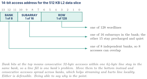
Decision 7, the pipeline and where ECC sits. Section 7.7 said correction cannot be inline, so the array delivers raw data speculatively and the syndrome resolves behind it.
| Cycle | What happens |
|---|---|
| 0 | bank arbitration, address decode, subarray select, wordline drive |
| 1 | develop 280 ps, sense 60 ps |
| 2 | 288 bits out of the macro, onto the return bus, syndrome trees start |
| 3 | data delivered to the requester and used, syndrome resolves |
| 4 | if any of the four syndromes is nonzero, squash the consumer, correct, replay, and write the corrected word back as a demand scrub |
Decision 8, redundancy and repair. Section 6.3 said unrepaired arrays cost double-digit yield. Add two spare columns per subarray plus memory BIST and fuse-programmed repair per DFT and Silicon Debug.
Decision 9, scrubbing. Section 7.9 said patrol scrubbing at a 24-hour period costs 48 accesses per second and removes three orders of magnitude of accumulated double errors. Add a background address counter that steals idle bank cycles.
Decision 10, the voltage floor. Section 4.3 said this array's Vmin is a six-sigma cell property, and it will be higher than the logic's. Either give the array its own rail or clamp the domain's DVFS floor to it, and record that number in the power intent so DVFS Droop and Thermal and the power controller respect it.
The whole design is ten decisions, each traceable to a physical fact, and nothing in it is arbitrary. That is what a good answer to this question looks like, and the shape of the reasoning matters more than whether your row count matches the interviewer's.
09.Part 10, check yourself
Answer out loud, in full sentences, as if an interviewer asked. If you cannot, reread the section named.
- Why can synthesis optimize your logic but not your memory, and what does that imply about the order in which you design a block containing an array? (1.1, 1.2)
- Draw a 6T cell, explain what each of the six transistors does, and then explain why the same cross-coupled structure that usefully stores a bit here is a hazard called metastability in a flip-flop. Use the three equilibria. (2.1, 2.2, 2.3)
- Compare SRAM and DRAM on devices per bit, area per bit, refresh, and destructive read. Why does the destructive read create a row buffer in DRAM and nothing analogous in SRAM? (2.4)
- Work out how long a full bitline swing takes against a 100 mV swing, with real capacitance and current numbers, use it to explain why sense amplifiers exist, then walk the four phases of a read and say why both bitlines are precharged and why sensing is differential rather than against a fixed reference. (3.1, 3.2, 3.3)
- Cache access time in nanoseconds has barely changed in twenty years while cache latency in cycles has roughly quintupled. Explain the mechanism. (3.4)
- Explain the read-stability versus write-margin conflict using cell ratio and pull-up ratio, show with numbers what happens when you widen the access transistor to fix writes, and then explain why that same conflict makes SRAM set the minimum operating voltage of the whole chip. Include the six-sigma yield argument. (4.2, 4.3, 4.4)
- A true 8-read 4-write array costs how much more area than a single-ported one, and why is the answer not twelve times? Give the four ways designs avoid paying it, and explain why a three-kilobyte register file is physically comparable to a much larger cache. (5.5, 5.6, 5.7)
- What is a half-selected cell, when does it exist, and which assist circuits make its situation worse? (4.5, 5.3)
- Derive from a counting argument rather than quoting it, solve it for 64 data bits, and state the resulting configuration and overhead. (7.3, 7.5)
- Show with an actual worked example what plain Hamming does to a double error, explain exactly what the extra overall parity bit buys, and say what SECDED still cannot handle. (7.4)
- When is parity enough and when is it not? Give the L1 instruction cache case and the write-back data cache case, and explain the tag array's false-hit versus false-miss asymmetry. (7.2, 7.8)
- ECC decode is roughly 270 ps against a 333 ps cycle. How is it kept off the critical read path, and what does that arrangement require the machine to already be able to do? (7.7)
- What is scrubbing, what failure does it prevent, and how does the uncorrectable rate scale with the scrub interval and with the upset rate? (7.9)
- A single particle now flips four adjacent cells. Why does that break SECDED, what is the fix, and why does the fix usually cost nothing extra? (6.2, 7.10)
- A whole DRAM device fails, and separately, NAND flash corrects hundreds of bits per codeword with less overhead than SECDED's 12.5 percent. Explain both, and say what the two have in common. (7.11)
10.Part 11, related notes
- Cache Organization and Prefetching for the sets, ways, and lines these arrays physically implement, and for the latency-hiding techniques that exist because of section 3.4
- Execution Units for the register file porting pressure of section 5.7 and for the bypass network that exists to avoid buying more read ports
- DVFS Droop and Thermal for what the array Vmin of Part 4 does to the whole chip's operating range
- Power Fundamentals and Clock Gating for the dynamic power equation used on bitline swing, and for the subarray-level gating that follows from it
- Clocking Reset and Domain Crossing for metastability, which is the middle crossing of section 2.3 seen in a flip-flop
- Digital Logic and Timing for the capacitance-and-delay model that every number in Part 3 comes from
- DFT and Silicon Debug for memory BIST, redundancy analysis, and fuse-based repair from section 6.3
- Out of Order Execution for the squash-and-replay machinery that makes the parallel ECC check of section 7.7 nearly free
- Load Store and Memory Ordering for the store path that the ECC granule and read-modify-write question in 7.5 lands on
- Cache Coherence Protocols for why a dirty line is the only copy, which is the argument that forces correction rather than detection
- DRAM and Memory Controllers for the vault's DRAM treatment, the contrast case for Part 2
- NVM, Storage, and Storage-Class Memory for the vault's NAND flash chapter, which is where the raw error rates of section 7.11 come from