DRAM Controllers, JEDEC Timing, and the DFI Interface
September 8, 2026133 min readadvanced
Every idea in this note descends from one physical fact, so start there and derive rather than assert.
01.Part 1, one capacitor, and everything that follows from it
1.1 The cell, and why it forgets
Every idea in this note descends from one physical fact, so start there and derive rather than assert.
A DRAM bit is one capacitor and one transistor. The capacitor holds charge or does not, and the transistor connects it to a long vertical wire called the bitline when a horizontal wire called the wordline is driven high. That is the entire cell. Compare it to the six-transistor SRAM cell in SRAM Arrays and ECC, which holds its value with a pair of cross-coupled inverters actively fighting to keep it. The SRAM cell is powered and self-correcting. The DRAM cell is a bucket.
Buckets leak. The capacitor's charge drains through the access transistor's subthreshold conduction, through junction leakage into the substrate, and through the dielectric. From Power Fundamentals and Clock Gating, subthreshold leakage rises roughly exponentially with temperature, so the leak gets much faster when the part gets hot. JEDEC's answer is a guaranteed retention window: every cell must hold a readable value for at least 64 ms at or below 85 °C for DDR4, halving to 32 ms above that. DDR5 assumes a 32 ms window as its baseline.
That single number generates a timing parameter you will meet again in Part 4. JEDEC does not ask the controller to name rows. It divides the retention window into 8192 REFRESH commands and requires that all 8192 be issued inside it, so the average interval between refresh commands is
for DDR4 at normal temperature, and
for DDR5, or for DDR4 running hot. Those are not arbitrary constants somebody chose. They are the retention window divided by the number of refresh commands the standard mandates inside it, and being able to say that out loud is a small but real signal.
Be exact about the 8192 if you are pushed on it, because the tempting simplification is wrong and it is a cheap thing to get right. 8192 is a command count, not a row count. Work it out for an 8 Gb DDR4 x8 part: 8 Gb is 1024 MB, divided across 16 banks is 64 MB per bank, divided by a 1 KB row is 65,536 rows in every bank. So one REFRESH command must internally refresh eight rows in each bank, not one, and a denser part refreshes more rows per command still. The controller never sees any of that, which is precisely why JEDEC counts commands rather than rows, and it is also the reason in Part 4.9 grows with density while does not.
1.2 Why reading needs an amplifier, with the charge-sharing arithmetic
Here is the part that is genuinely surprising the first time, and it is worth doing with numbers before any abstraction.
The storage capacitor is small. Public figures for recent processes put it in the region of 20 to 30 femtofarads, and it has been held near that value for many generations because the sensing scheme stops working if it shrinks much further. The bitline it must drive is long, running past thousands of other cells, and its capacitance is several times larger, commonly quoted at 100 to 300 fF.
Take fF, fF, and a supply of 1.2 V. Before a read the bitline is precharged to half the supply, 0.6 V, and left floating. Now raise the wordline. The access transistor turns on and the cell capacitor, sitting at 1.2 V for a stored one, shares its charge with the bitline. Charge is conserved, so the final voltage is the total charge divided by the total capacitance.
The bitline moved from 0.600 V to 0.6545 V. The entire signal is 54 millivolts, and for a stored zero it swings the same 54 mV downward. Nothing in a logic gate can read that. So every bitline terminates in a sense amplifier, a cross-coupled pair that is switched on after the charge sharing has settled and that amplifies whichever side is higher into a full rail-to-rail difference. This is the same device, doing the same job for the same reason, as the SRAM sense amplifier in Part 3 of SRAM Arrays and ECC. The difference is that the SRAM cell keeps driving its bitlines while the DRAM cell has already given up everything it had.
Two consequences follow immediately and both matter.
The read is destructive. After charge sharing the cell no longer holds 1.2 V, it holds 0.6545 V, which is not a stored one by any definition. The value has been consumed by the act of reading it. What saves the data is that the sense amplifier, once it has resolved, drives the bitline hard to the full rail, and the access transistor is still on, so the cell is written back to full strength by the same amplifier that read it. Reading a DRAM row is really read-amplify-restore, and the restore is not instantaneous. That is the physical content of , which Part 4 will name.
Precharge is a real operation with a real cost. Before the next read the bitline must be returned to exactly half the supply everywhere along its length, because the 54 mV signal is measured against that reference and a bitline left at the previous value would swamp it. Driving a long, heavily loaded wire to a precise mid-rail value and letting it settle is the physical content of .
1.3 The row buffer is the row of sense amplifiers
The cells are laid out in a rectangular array. A wordline runs horizontally across thousands of cells, each of which hangs off its own vertical bitline, and each of those bitlines has its own sense amplifier at the edge of the array.
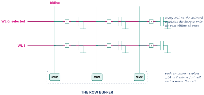
The strip of sense amplifiers now holds every bit that was on that wordline. In DDR4 and DDR5 a row is commonly 1 KB or 2 KB per device, and the strip is called the row buffer, the open page, or the open row depending on who is talking. All three mean the same thing.
Now the fact that reorganises everything. Getting a row into the row buffer is expensive. Getting a column out of an already-open row buffer is cheap. The expensive part is the physics of Part 1.2, the charge sharing and the amplification and the restore. The cheap part is a multiplexer selecting some bits out of a strip of latched, full-rail values. So a memory system's performance is dominated not by how much data you move but by how often you have to move a new row into the buffer, which is Part 3 and, transitively, the entire rest of this note.
1.4 The three commands, before any timing
A DRAM device is a slave. It has no idea what an address means and never issues anything on its own. The controller sends commands on a command/address bus and the device obeys. Three commands carry essentially all the traffic.
ACTIVATE, usually written ACT, takes a bank number and a row number and performs the read-amplify-restore of Part 1.2. After it completes, that bank's row buffer holds that row and the bank is said to have an open row.
READ and WRITE, usually written RD and WR, take a bank number and a column number and move a burst of data between the row buffer and the data pins. They do not touch the array. They require the bank to already have the right row open, and it is the controller's job to guarantee that. If the controller issues a READ to a bank whose open row is the wrong one, the device does not complain, it returns the wrong data.
PRECHARGE, usually written PRE, closes the open row and returns the bitlines to mid-rail so the bank is ready for a different ACTIVATE.
Two more commands round out the set for now. REFRESH, REF, is Part 7. NOP or deselect is the absence of a command, and a real command bus spends most cycles doing exactly that.
There is no cache, no reordering, no protection, and no error signalling in the device. Every one of those functions, if it exists at all, lives in the controller. Say that plainly in an interview, because a surprising number of candidates describe DRAM as though it were an intelligent peer.
02.Part 2, how a DRAM part is organised
2.1 Banks, and the number that justifies them
Suppose a device had exactly one array with one row buffer. Then every access that wanted a different row would have to precharge, activate, and read, in that order, with no overlap possible, because there is only one set of sense amplifiers and one wordline driver.
Put a number on how bad that is. Using JEDEC DDR4-3200 as the running example throughout this note, with a clock period ns, the minimum time between one ACTIVATE and the next ACTIVATE to the same bank is , about 45.75 ns. One column read of a burst of eight on a 64-bit channel delivers 64 bytes and occupies the data bus for four clocks, , which is 2.5 ns.
So a single bank doing one 64-byte access per row activation delivers
against a channel peak of GB/s. One bank can fill about five and a half percent of the bus. To saturate the bus under that access pattern you need
banks working concurrently, each one in a different phase of its own activate-read-precharge cycle so that their data bursts interleave back to back on the shared bus.
That derivation explains a fact about the standards that otherwise looks like arbitrary escalation. DDR3 x8 devices have 8 banks. DDR4 x8 devices have 16, arranged as four bank groups of four. DDR5 doubled it again to 32, as eight groups of four. Nobody added banks for capacity, since banks do not add bits. They added banks because did not shrink while the data rate kept doubling, so the number of concurrent activations required to keep the bus busy kept climbing. Note the honest consequence, which is that even 16 banks is short of 19, and Part 4.8 will show a second constraint that binds before the bank count does.
Physically, a bank is an independent array with its own row decoder, its own sense-amplifier strip, and its own row-open state. Banks share the command bus, the address bus, and the data bus. That sharing is the whole game: the controller can have many banks busy internally at once, but only one command can be issued per command-bus slot and only one burst can be on the data bus at a time. Bank parallelism is latency overlap, not bandwidth multiplication.
2.2 Bank groups, and why DDR4 had to invent them
Bank groups are the one piece of DRAM organisation that people get wrong most often in interviews, and the reason they exist is worth working through rather than memorising.
By DDR4 the external data rate had reached 1.6 to 3.2 gigatransfers per second, so a burst of eight occupies only 2.5 ns of bus time. But the shared circuitry inside the device that reads a row buffer, muxes out the selected columns, serialises them, and drives them to the pins does not run anywhere near that fast. It runs at a lower internal frequency and works on a wide word, which is the prefetch architecture: DDR4 fetches 8 bits per pin per column access, DDR5 fetches 16. The internal path from a bank's sense amplifiers to the serialiser therefore has a recovery time, and that recovery time is longer than at high data rates.
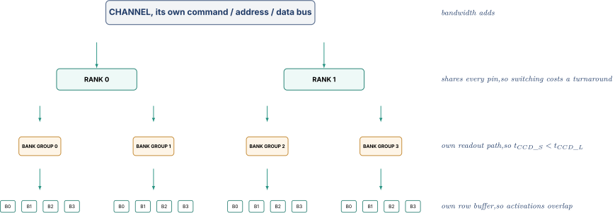
The fix is to replicate the shared path. Divide the banks into bank groups, and give each group its own local sense-amplifier readout path. Now two column accesses to different bank groups can be issued back to back at the full bus rate, because they use different internal paths, while two column accesses to the same bank group must be spaced further apart, because they share one.
That is why almost every DDR4 and DDR5 timing parameter comes in two flavours, a short one for different bank groups and a long one for the same bank group.
| Parameter | Meaning | Short version | Long version |
|---|---|---|---|
| column access to column access | , different group | , same group | |
| activate to activate | , different group | , same group | |
| write to read turnaround |
For DDR4, equals the burst length in clocks, four clocks for a burst of eight, so a controller that alternates bank groups can issue a column command every single burst and keep the data bus completely full. is materially longer, and JEDEC specifies it in exactly the two-term form Part 4.1 unpacks, . At DDR4-3200 the nanosecond term wins, so is 8 clocks, twice . At DDR4-1600 the CK term wins instead and it is 5 clocks, only a quarter longer than the short version. The penalty for ignoring bank groups therefore gets worse as the part gets faster, which is the same divergence as everywhere else in this note and is worth noticing rather than memorising either number.
The design consequence is concrete and is the correct answer to "what do bank groups change in your scheduler." The address mapping should place the bank-group bits low enough that a sequential stream walks across groups, and the command scheduler should prefer a ready command in a different bank group over an equally ready command in the same one. A controller that ignores bank groups can lose a large fraction of peak bandwidth on a perfectly sequential stream without a single row miss, which is the counterintuitive part worth saying out loud.
2.3 Ranks, channels, and subchannels
Above the device there are three more levels and they are frequently confused.
A rank is a set of DRAM devices that are selected together by one chip-select and that respond in lockstep to produce the full channel width. Eight x8 devices in a rank give a 64-bit data path. Sixteen x4 devices do the same. Every device in a rank sees the same command at the same time and contributes its slice of every burst. Ranks share all the pins, so switching between ranks costs a bus turnaround penalty, but they provide independent bank state, so a second rank roughly doubles the number of banks the controller can juggle.
A channel is a complete, independent memory interface: its own command bus, its own address bus, its own data bus, and its own controller. Two channels are two memory systems that happen to share an address space. Their bandwidths add.
DDR5 adds a level that did not exist before. A DDR5 DIMM presents its 64 data bits as two independent 32-bit subchannels, each with its own command and address bus and its own bank-group hierarchy. This is not cosmetic. A burst of sixteen on a 32-bit subchannel delivers bits, which is exactly 64 bytes, exactly one cache line. So DDR5 doubled the number of independently addressable memory pipes without changing the granularity at which a cache line arrives, which is a far better answer to "what did DDR5 actually change" than "it is faster."
2.4 A concrete address decomposition, with small numbers
Abstract hierarchy is useless until you decode an address by hand, so build a deliberately tiny device that fits on a page.
The toy device. Four banks. Eight rows per bank. Eight columns per row. Each column access delivers one 64-byte cache line.
Compute the capacity from the bottom up. One row is bytes. One bank is bytes. The device is bytes, so a physical address is 14 bits, .
Now the fields. Six bits, , are the byte offset inside the 64-byte line and never reach the DRAM at all, because the smallest thing the memory system moves is a whole line. Three bits select one of eight columns. Three bits select one of eight rows. Two bits select one of four banks. That is bits, and it accounts for every one.
What the controller must decide is which address bits get assigned to which field. Nothing in the DRAM cares. The device sees a bank number, a row number, and a column number on its pins, and it has no opinion about where they came from. The mapping is entirely a controller design choice, it is a pure combinational function, and Part 5.2 shows that it is worth roughly an order of magnitude of performance on realistic traffic.
Take the natural-looking assignment first, the one almost everyone writes down without thinking, with the fields in the order row, bank, column, offset from the most significant bit down.
| Field | Bits | Width |
|---|---|---|
| row | 3 | |
| bank | 2 | |
| column | 3 | |
| byte offset | 6 |
Decode address . All bits zero, so row 0, bank 0, column 0.
Decode address , which has only bit 12 set. Then , so row 2. , so bank 0. , so column 0.
So addresses 0 and 4096 land in the same bank and different rows. Hold onto that, because it is about to cost a factor of ten in Part 5.2.
03.Part 3, the row buffer is a cache, and that is the whole model
3.1 Three outcomes, priced individually
An access arrives at a bank. There are exactly three possibilities and they are not equally spaced.
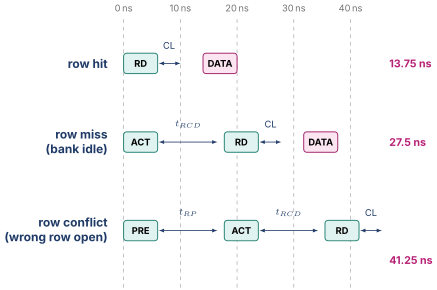
Row hit. The bank already has this row open. Issue RD, wait for the data to appear on the pins, done. At DDR4-3200 with CL 22, that is ns.
Row miss, sometimes called a row-empty or idle-bank access. The bank has no row open, because the last access precharged it. Issue ACT, wait , issue RD, wait . At CL 22 and 22 that is ns.
Row conflict. The bank has the wrong row open, and only one row can be open per bank because there is only one sense-amplifier strip. Issue PRE, wait , issue ACT, wait , issue RD, wait . That is ns.
Three to one, best case to worst, from the device alone. The numbers happen to fall in a clean ratio at the 22-22-22 speed bin because the three parameters are equal there, which is a common but not universal arrangement.
The distinction between a miss and a conflict is the one that gets probed, so be exact about it. A miss finds the bank clean and pays only for opening. A conflict finds the bank dirty and pays for closing first. They are not the same event, and a controller policy that produces many misses can easily be better than one that produces many conflicts, which is precisely the open-page versus closed-page argument in Part 6.3.
3.2 Averaging it, and why the device number is the floor and not the answer
Give a workload a hit rate , a miss rate , and a conflict rate with . The average device latency is
Three workloads, worked.
Perfectly sequential streaming through a well-mapped address space gives near 0.9, so ns. Pointer chasing through a large graph gives essentially , so ns, 2.7 times worse for exactly the same hardware. A mixed workload at , , gives ns.
Now be honest about what that number is and is not, because this is where a good interviewer separates people who have read about DRAM from people who have measured it. The device latency is the floor. Publicly measured idle memory latency on modern desktop parts lands broadly in the 60 to 90 nanosecond range, and the DRAM device accounts for well under half of it. The rest is the last-level-cache miss handling, the on-chip fabric traversal in both directions from Interconnect and AMBA, the controller's own queueing and scheduling pipeline, the PHY's serialisation and deserialisation, and the fill path back into the cache from Cache Organization and Prefetching. Under load, queueing delay at the controller can exceed every other term combined, because a queue with a utilisation approaching one has an unbounded waiting time.
The sentence to have ready is: the JEDEC parameters set the floor, the scheduler decides how close to the floor you get, and the fabric and the queue decide what the core actually sees.
3.3 Why every later decision is downstream of this one
Everything in Parts 5 through 8 is an attempt to move requests up the picture in 3.1. Address mapping decides which requests land in the same bank and therefore whether they conflict. Scheduling decides the order, and reordering to group same-row requests converts conflicts into hits. Open-page versus closed-page policy is a bet about whether the next request to this bank will hit. Quality of service is the question of whose requests get to be converted into hits when they compete.
Say this once and mean it, because it is the framing that makes the rest of a memory-controller interview coherent rather than a parameter quiz. A DRAM controller is a machine for maximising row-buffer reuse subject to a large set of timing constraints and a fairness requirement. Every mechanism in the rest of this note is one of those three words.
04.Part 4, the JEDEC timing parameters, one at a time
4.1 What a timing parameter is, and how to read one
A JEDEC timing parameter is a minimum separation between two commands, expressed either in nanoseconds, in clock cycles written CK, or as the maximum of the two. The device does not enforce them. If the controller issues a command early, the device does something undefined, and undefined for an analogue sense amplifier means corrupted data rather than a clean error. There is no handshake, no ready signal, and no retry. The controller is solely responsible for legality, and that responsibility is the single largest source of RTL in the design.
The "maximum of CK and nanoseconds" form catches people out, so unpack it. specified as means the constraint has two independent physical origins. The nanosecond term is analogue physics inside the array, which does not care what your clock is doing. The clock-cycle term is a digital pipeline inside the device that needs a fixed number of internal beats. Whichever is larger at your operating frequency is the one that binds, and which one binds changes with the speed bin. At a slow clock the CK term dominates. At a fast clock the nanosecond term does. A controller must compute both and take the maximum, and it must do so per frequency point, because a good controller supports several. That is a small but real piece of arithmetic in the RTL and it is worth mentioning unprompted.
Everything below uses JEDEC DDR4-3200 at the 22-22-22 bin, ns as the running example, because it is public, widely tabulated, and round enough to do in your head.
4.2 , RAS to CAS delay
The constraint. From an ACTIVATE to the first READ or WRITE to that bank.
The physics. This is exactly the interval Part 1.2 described: raise the wordline, let the cell share its charge onto the bitline, wait for that 54 mV to develop, fire the sense amplifiers, wait for them to resolve to full rail. Only when the row buffer holds valid full-rail data can a column be selected out of it.
The value. 22 clocks, 13.75 ns. Notice that this has barely moved in absolute time across four DRAM generations, because it is governed by charge sharing on a bitline and not by any digital pipeline. Data rates went up several-fold and went down by a few nanoseconds. That divergence is the memory wall of Cache Organization and Prefetching expressed as a single parameter.
4.3 , also written CL, the column access latency
The constraint. From a READ to the first bit of data on the DQ pins.
The physics. Decode the column address, mux the selected bits out of the row buffer, route them across the die to the output path, serialise them at the pin rate, and drive the pads. Notice that this is a digital pipeline, not an analogue settling time, which is why CL is specified in clocks and why its value in clocks rises steadily with each speed bin while its value in nanoseconds stays roughly flat. DDR4-2133 CL 15 is 14.1 ns. DDR4-3200 CL 22 is 13.75 ns. The number people quote on enthusiast forums went up by seven and the latency went slightly down.
There is a matching CWL, CAS write latency, for writes. It is generally smaller than CL because the write path is shorter, and a controller must track both because they determine when the data bus is occupied and in which direction.
4.4 , row precharge time
The constraint. From a PRECHARGE to the next ACTIVATE to that bank.
The physics. Turn off the wordline, then drive every bitline in the bank back to exactly half the supply and let it settle. The 54 mV signal of Part 1.2 is measured against that reference, so the reference has to be right to within a few millivolts along a wire running past thousands of cells. That is the whole cost.
The value. 22 clocks, 13.75 ns.
4.5 and , the row cycle
is the minimum time from an ACTIVATE to the PRECHARGE of the same bank, and it is the first of three parameters in the set that are floors on how quickly you may close a row rather than floors on how quickly you may act. The other two are in 4.6 and in 4.7, and the legal precharge instant is the latest deadline any of them imposes, never the earliest.
The physics is the restore. Part 1.2 established that reading destroys the cell, and that what saves the data is the sense amplifier driving the bitline hard and writing the cell back through the still-open access transistor. Restoring a capacitor through a resistive access transistor takes time. Precharge before the restore has finished and you have written a weak, marginal value back into every cell on that row, which will fail retention early and produce a bit flip minutes later somewhere else entirely. That is the failure mode, and note what kind of failure it is: not a timing error visible on a scope, but silent data corruption with a long delay fuse.
The value. 32 ns for DDR4-3200, which is 51.2 clocks and therefore 52 clocks after rounding up. Note that it is not equal to the other three, and note that , which means a bank that opened a row and immediately read from it must still wait a little longer before it is allowed to close.
, the row cycle time, is the ACTIVATE-to-ACTIVATE minimum for the same bank and is simply
This is the parameter that generated the 19-bank result in Part 2.1 and it is the most important single number in the set, because it is the throughput limit of one bank.
4.6 A worked command timeline
Put the parameters on one picture and walk it, because the interaction between and is where a hand-drawn schedule usually goes wrong.
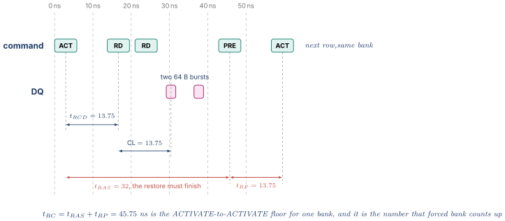
Two things in that picture are easy to get wrong on a whiteboard and are worth rehearsing.
First, is measured from the ACTIVATE, not from the last READ, so a bank that opens a row and reads once still cannot close for the full 32 ns even though it has been idle for most of it. Closing early is not slow, it is illegal.
Second, there is a separate constraint the picture only hints at. , read to precharge, is the minimum from a READ to a PRECHARGE of the same bank, because the column data must finish leaving the row buffer before the bitlines are yanked to mid-rail. The legal precharge time is therefore the later of the deadline and the deadline, and a controller that tracks only one of them will occasionally issue an early precharge. In RTL this is not an if-else, it is a set of independent countdown timers per bank whose expiry flags are ANDed into a single pre_legal signal, and that structure generalises to every parameter in this part.
4.7 , and why writing is worse than reading
The constraint. , write recovery, runs from the end of the write data burst to the PRECHARGE of that bank. DDR4 specifies 15 ns.
The physics. A write does not put a value in the row buffer and stop. It drives the sense amplifier to the new value, the sense amplifier drives the bitline, and the bitline charges the cell capacitor through the access transistor. That last step is charging a capacitor through a resistance and it is slow. Precharge before it completes and the cell holds an intermediate voltage, which is the silent-corruption failure of 4.5 again wearing different clothes.
Note the asymmetry that follows, because it is worth naming explicitly. A read finishes at the pins and a write finishes in the array. A read's cost is visible as latency and the controller can pipeline around it. A write's cost is invisible as latency, because nobody is waiting for a write to complete, but it occupies the bank for a long time after the data has gone by. That is why write-heavy traffic hurts a memory system more than its bandwidth share suggests, and it sets up Part 6.4.
4.8 and , and the power-delivery argument
These two are the most interesting parameters in the set because neither of them is about the array's logical ability to do the work.
, row-to-row delay, is the minimum between two ACTIVATE commands to different banks. Different banks are independent arrays with their own decoders and their own sense amplifiers, so logically there is no reason at all why they cannot activate simultaneously. The reason they cannot is current.
Work out how much. A DDR4 device with a 1 KB page and a x8 organisation raises one wordline and sense-amplifies 8192 cells at once, since a kilobyte is 8192 bits. That numeral is the same as the refresh-command count in Part 1.1 and has nothing to do with it, which is worth noticing once so the coincidence never trips you. Each of those sense amplifiers takes a bitline that has settled at mV and drives it hard to a full rail, and each bitline is a few hundred femtofarads. Every one of those transitions happens in the same few nanoseconds, because the whole point of a sense-amplifier strip is that it fires as one. Reach for the machinery of Power Fundamentals and Clock Gating, but reach for the right quantity out of it. What the device's power delivery cannot supply is current, so the number to compute is the charge and not the energy . With 8192 bitlines at 250 fF and 1.2 V, one activation moves on the order of
If that charge moves in roughly 10 ns the average current is around 250 mA, and the instantaneous peak is higher. That is a large transient for a small package with limited decoupling, drawn through the same package inductance that produces the droop of DVFS Droop and Thermal. Treat that arithmetic as an order-of-magnitude illustration rather than a datasheet figure, since real devices segment the array and stage the sensing precisely to spread the transient, but the shape of the argument is right and it is the argument JEDEC is encoding.
So JEDEC caps the rate. enforces a minimum gap between any two activations. And then , the four activate window, enforces something stronger and stranger: no more than four ACTIVATE commands may be issued in any rolling window of nanoseconds, across the entire device, regardless of which banks they target.
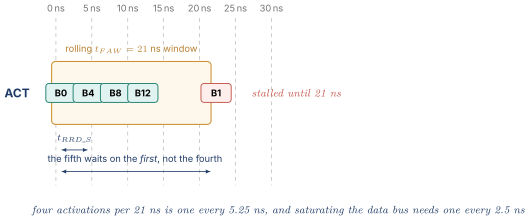
The exact values depend on page size and speed bin, which is itself the giveaway. At DDR4-3200 JEDEC tabulates ns and gives in three page-size columns: 13 ns for a half-kilobyte page, 21 ns for one kilobyte, and 30 ns for two. is indexed by page size. A purely logical constraint would not care how wide the row is. A charge-per-activation constraint has to, because a 2 KB page sense-amplifies twice as many cells and therefore moves twice the charge. Note that the numbers move with page size without doubling with it, 21 to 30 rather than 21 to 42, which is what you would expect from a window that must also stay wide enough to hold four activations at all. Do not oversell the scaling as linear. That indexing is the evidence that the parameter is about power delivery, and saying so is a much better answer than reciting the definition.
Now price it, because this is the number that lands.
Four activations per 21 ns is one activation every 5.25 ns. Under fully random access every activation yields exactly one 64-byte column read, so the achievable rate is
against a DDR4-3200 channel peak of 25.6 GB/s. alone caps random-access bandwidth at about 48 percent of peak, before considering refresh, bus turnaround, or any scheduling inefficiency whatsoever. And notice that it agrees with the independent derivation in Part 2.1: saturating the bus needs one column access every ns, and percent. Two different arguments, one from bank cycle time and one from activation rate, converge on the same answer, which is a good sign the model is right.
The design conclusion is the one that matters. Adding banks past a certain point buys nothing under random access, because binds before the bank count does. What buys something is improving locality so that each activation yields more than one column access, which is the entire justification for address mapping in Part 5.2 and open-page policy in Part 6.3.
4.9 and , refresh in the parameter set
was derived in Part 1.1 from the retention window divided by the row count: 7.8125 µs for DDR4 at normal temperature, halving above 85 °C, and 3.906 µs as the DDR5 baseline.
is the refresh cycle time, the interval during which the device is busy servicing a REFRESH and will accept no other command. It is large and it grows with density, because a single all-bank REFRESH internally activates and restores a row in every bank and a denser part has more to do. Widely published values are 350 ns for an 8 Gb DDR4 device and 550 ns for 16 Gb, and 295 ns for a 16 Gb DDR5 device under the standard all-bank scheme. Refresh gets its own part, Part 7, because the controller's freedom to schedule it is where the engineering lives.
4.10 The full set, and the honest advice about memorising it
| Parameter | From | To | DDR4-3200 value | What it physically is |
|---|---|---|---|---|
| ACT | RD or WR, same bank | 13.75 ns | charge sharing plus sense-amp resolution | |
| CL, | RD | first data on DQ | 13.75 ns | column mux, routing, serialisation |
| CWL | WR | first data on DQ | shorter than CL | the write path is shorter |
| PRE | ACT, same bank | 13.75 ns | driving bitlines back to mid-rail | |
| ACT | PRE, same bank | 32 ns | the restore must complete | |
| ACT | ACT, same bank | 45.75 ns | , the bank throughput limit | |
| RD | PRE, same bank | around 7.5 ns | column data must clear the buffer | |
| end of write data | PRE, same bank | 15 ns | the cell capacitor must charge | |
| end of write data | RD | around 2.5 / 7.5 ns | internal write path must clear | |
| RD or WR | RD or WR | 4 clocks / 8 clocks | shared readout path per bank group | |
| ACT | ACT, different banks | around 3.3 / 4.9 ns | activation current | |
| 1st ACT | 5th ACT | around 21 ns, 1 KB page | activation charge budget | |
| REF | any command | 550 ns at 16 Gb | internal refresh of every bank | |
| REF | REF, average | 7.8 µs | retention window over 8192 mandated REF commands |
Two pieces of honesty about this table are worth stating out loud in an interview rather than hiding.
Do not memorise the numbers. They change with every speed bin, every density, every page size, and every generation, and the authoritative tables live in JESD79-4 for DDR4 and JESD79-5 for DDR5. What you should be able to do without a datasheet is name what each parameter physically encodes, say which mechanism it comes from, and predict which direction it moves when the part gets denser, hotter, or faster. That is the knowledge that transfers, and it is what a designer actually needs, because the RTL reads its values from configuration registers anyway.
Know which ones are shrinking and which are not. The parameters governed by digital pipelines, CL and CWL and the CK terms, scale with the clock. The parameters governed by analogue physics inside the array, and and and , have been approximately flat in nanoseconds for a decade and is getting worse with density. That divergence is why controller quality matters more every generation, not less. When the data rate doubles and does not move, the cost of a row conflict measured in lost transfers doubles.
05.Part 5, inside the controller
5.1 The two queues, and why there are two
A memory controller is not one pipeline. It is two queues with a translation between them, and understanding why they are separate is most of understanding the block.
The transaction queue, sometimes called the request queue or the pending-transaction buffer, holds requests as the rest of the chip described them: an address, a size, a read or write flag, a client identifier, a quality-of-service class, and an identifier the response must carry back. Its entries are protocol objects that arrived over AXI or CHI from Interconnect and AMBA. It knows nothing about rows or banks.
The command queue holds DRAM commands: ACT to bank 5 row 219, RD to bank 5 column 12, PRE to bank 5. Its entries are things that can be placed on the command bus in a single slot. One transaction becomes between one and three commands depending on the state of its bank, and sometimes more if the access has to be split.
Between them sits the address mapper, a purely combinational function turning a physical address into a channel, rank, bank group, bank, row, and column. It is one of the very few parts of a memory controller that is not a state machine, and it is the subject of 5.2.
Around them sit three more things. A per-bank state tracker holding, for every bank, whether a row is open and which one, plus a set of countdown timers implementing the parameters of Part 4. A command arbiter choosing which of the currently-legal commands to issue this slot, which is Part 6. And a data path with the write data buffer, the read return buffer, ECC generation and checking, and the crossings to the PHY, which is Part 10.
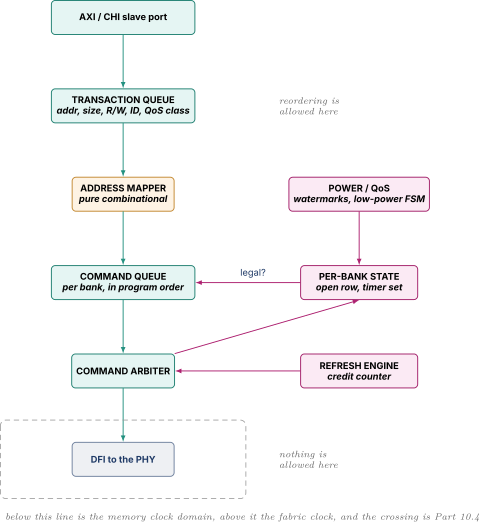
The reason the two queues are separate is worth being able to state crisply. Reordering must happen at the transaction level, because that is where the memory model constraints live, and legality must be enforced at the command level, because that is where the JEDEC parameters live. Mixing them produces a design where you cannot reason about either. It also means the controller has to enforce the ordering rules of Load Store and Memory Ordering itself: two accesses to overlapping addresses may not be reordered relative to each other, so the transaction queue needs an address-overlap check on insertion, which in practice is a small content-addressable memory of exactly the kind in Arbiters FIFOs and CAMs.
5.2 Address mapping, and the factor of ten hiding in it
Return to the toy device of Part 2.4: four banks, eight rows, eight columns of 64 bytes, 16 KB total, 14 address bits.
The stream. Two clients are running at once, which is the normal case on any SoC. Client A streams sequentially from address 0. Client B streams sequentially from address 4096. Their requests arrive interleaved, A0, B0, A1, B1, and so on, because the fabric is round-robining between two masters. Each reads eight consecutive 64-byte lines, so there are sixteen requests in total and they cover 1 KB.
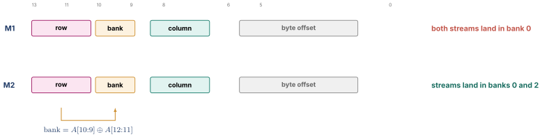
Mapping M1, the obvious one. Fields in the order row, bank, column, offset, so row is , bank is , column is , offset is .
Client A's eight addresses are 0, 64, 128, ..., 448. All of them have , so all eight are bank 0, row 0, columns 0 through 7.
Client B's eight addresses are 4096, 4160, ..., 4544. All of them have and nothing else above bit 8, so and . All eight are bank 0, row 2, columns 0 through 7.
Now interleave them. A0 opens bank 0 row 0 and reads. B0 wants bank 0 row 2, which is a row conflict: precharge, activate, read. A1 wants row 0 again, another conflict. Every single one of the sixteen requests after the first is a row conflict, and they are all in one bank so nothing overlaps with anything.
Fifteen of sixteen banks are idle throughout. This is the classic bank thrashing pathology and it is entirely a consequence of where the bits went.
Mapping M2, XOR the bank index with row bits. Keep every field where it was, but compute the bank index as
Recompute. Client A at address 0: , , so bank , row 0. Client B at address 4096: , , so bank , row 2.
The two streams now live in different banks. Client A occupies bank 0 with row 0 open and gets eight consecutive row hits after one activation. Client B occupies bank 2 with row 2 open and does the same. The two activations happen in different banks and overlap.
Row hit rate went from 0 to 14 out of 16, which is 87.5 percent, and the elapsed time fell by a factor of about eleven, for exactly the same request stream on exactly the same silicon. Nothing changed except which address bits were wired into the bank decoder. That is why the address map is the highest-leverage single decision in a memory controller and why it is a configurable register in every commercial one.
Four rules generalise out of that example and they are the answer to "how would you choose an address map."
Put the bits that change fastest into the fields whose reuse you want. Column bits should sit immediately above the line offset, so that a sequential stream walks columns of one open row and hits.
Put the bank and bank-group bits immediately above the column bits. Then a stream that runs past the end of one row lands in a different bank, so the next activation overlaps with the current row's remaining accesses instead of serialising behind them. Putting bank-group bits at the very bottom, below the column bits, is also a defensible choice on some designs because it maximises opportunities, and choosing between those two is a real trade-off, not a solved problem.
Never put bank bits at the top. If bank is the most significant field, an entire contiguous region of the address space lives in one bank and every stream inside it serialises.
Break power-of-two aliasing with an XOR. Real address streams are full of power-of-two strides: frame buffers, matrix rows, page-aligned allocations, and per-thread stacks. Any of those can put two hot streams in the same bank with a plain field split. Folding some high-order bits into the bank index with an XOR scatters them, at the cost of a handful of gates and a small amount of debug pain, because a physical address no longer maps to a bank in a way you can compute in your head. The technique is public and long-standing in the literature on permutation-based interleaving, and it is standard practice.
The honest caveat to add unprompted: there is no universally best map, because it depends on the traffic. A GPU streaming a frame buffer, a CPU chasing pointers, and a display engine reading scanlines want different things. Which is why every commercial controller makes this a configuration register and why bringing up a new SoC includes a campaign of measuring candidate maps against real traces.
5.3 The per-bank timing tracker, which is where the RTL actually is
If you are asked to design a memory controller on a whiteboard, this is the structure to draw, because it is the part that is genuinely a logic design problem rather than a policy discussion.
For every bank in the system the controller holds:
- a valid bit, meaning a row is open
- the open row number
- a set of countdown timers, one per constraint that gates a future command on this bank
The timers are ordinary down-counters loaded with the configured parameter value when the relevant command issues, decrementing every memory clock, and saturating at zero. A command to this bank is legal when every timer that gates it reads zero. So the ACTIVATE-legal condition for bank is roughly
assign act_legal[b] = (rp_timer[b]   == 0)   // tRP since PRECHARGE
                    & (rc_timer[b]   == 0)   // tRC since last ACTIVATE
                    & (rrd_timer     == 0)   // tRRD, device-wide
                    & (faw_ok)               // tFAW rolling window
                    & (rfc_timer     == 0)   // tRFC since REFRESH
                    & ~bank_open[b];
Two of those deserve comment because they are the ones that trip designers up.
is not per bank. It is a device-wide constraint on the activation rate, so it is one counter shared by every bank, and the short-versus-long distinction means you need two of them plus knowledge of which bank group the previous activation hit.
is not a counter at all in the naive sense. It is a rolling window over the last four activations, so the natural structure is a four-entry shift register of timestamps, or equivalently a four-deep FIFO of countdown timers where a new activation is legal only if the oldest entry has expired. That is a small, elegant piece of RTL and it is a good thing to be able to draw, because it is exactly the kind of "state machines and arbitration" these roles name.
The scale is worth stating. Two ranks of a DDR5 device at 32 banks each is 64 banks, each with roughly eight to twelve timers of five to eight bits. That is on the order of five thousand flops of pure timing bookkeeping, all of it toggling constantly, all of it in the memory clock domain. It is also an excellent clock-gating target, because the timers for an idle bank are all at zero and will stay there, and gating a saturated down-counter costs nothing functionally. Raising that unprompted is a strong move for a candidate whose background is low power, and it connects directly to Power Fundamentals and Clock Gating.
The other thing to say is that this block is the natural home for assertions. Every JEDEC parameter is a temporal property of the form "command X shall not be issued within cycles of command Y," which is exactly the shape SystemVerilog assertions were built for.
The tempting first draft is to write it directly as a temporal sequence, something of the shape "a PRECHARGE, then no ACTIVATE for t_rp_cfg cycles." That draft does not survive contact with the language, and knowing why is the point. SystemVerilog's cycle-delay ranges and $past both require a compile-time constant delay, and is a runtime-configured register because a real controller supports several frequency points. So the check has to be built on a counter instead, and the counter has to be the checker's own rather than the design's, or a bug in the design's timer silently exonerates itself. That is precisely the independence argument from Part 2.4 of Verification Methodology, and here is the shape it produces.
// Shadow timer, owned by the checker, never shared with the design.
always_ff @(posedge mclk or negedge rst_n)
  if      (!rst_n)         chk_rp[b] <= '0;
  else if (pre_issued[b])  chk_rp[b] <= t_rp_cfg;      // reload on PRECHARGE
  else if (|chk_rp[b])     chk_rp[b] <= chk_rp[b] - 1; // saturate at zero

// No ACTIVATE to a bank until tRP has elapsed since that bank's PRECHARGE.
property p_trp;
  @(posedge mclk) disable iff (!rst_n)
    act_issued[b] |-> (chk_rp[b] == 0);
endproperty
assert property (p_trp);
Every other parameter in Part 4 is the same eight lines with a different reload condition, which is why this block is the most assertion-dense thing in the design. Naming the constant-delay wrinkle unprompted is itself a good signal: a candidate who has actually written these knows that runtime-configurable timing parameters are the awkward part of asserting them, and a candidate who has not will confidently write the sequence form that does not elaborate.
5.4 Where the rest of the design lives
Rounding out the block, because an interviewer will ask what else is in there.
The write data buffer holds write payloads from acceptance until the scheduler decides to drain them. It is usually much larger than the read return buffer, because writes can be deferred and reads cannot.
The read return path reassembles bursts, reorders responses back into whatever order the protocol requires, and drives responses onto the fabric. Under AXI, responses on a given ID must return in order while different IDs may interleave, so this is a reorder structure keyed by ID.
The ECC block generates check bits on the write path and checks and corrects on the read path, and it is on the critical latency path for every read, which is Part 11.
The refresh engine maintains the refresh credit and injects REFRESH commands into the arbiter, which is Part 7.
The low-power controller owns the transitions into and out of the DRAM's power-down and self-refresh states, and it is a state machine with sequencing obligations of exactly the shape in Part 7.4 of Power Fundamentals and Clock Gating. It is also where UPF matters, because the controller usually sits in a domain that can be retained or powered down while the DRAM stays in self-refresh, and the isolation and retention strategy for that boundary is written in the power intent file.
The initialisation and training sequencer brings the DRAM up from reset, programs its mode registers, and runs or supervises the training of Part 10.3.
06.Part 6, scheduling
6.1 FCFS, and exactly what it costs
The simplest possible scheduler issues commands in arrival order. Take four requests arriving in this order, all to the same bank:
| Order | Row | Column |
|---|---|---|
| 1 | 12 | 3 |
| 2 | 40 | 1 |
| 3 | 12 | 5 |
| 4 | 12 | 9 |
Under first-come first-served, request 1 activates row 12 and reads. Request 2 conflicts, so precharge, activate row 40, read. Request 3 conflicts again, so precharge, activate row 12, read. Request 4 now hits. That is one miss, two conflicts, one hit, and using the Part 3.1 costs the device time is roughly ns.
Now reorder to 1, 3, 4, 2. Request 1 misses and opens row 12. Requests 3 and 4 hit. Request 2 conflicts once. That is ns, a 22 percent improvement from nothing but permutation, and the improvement grows with queue depth because there are more same-row requests to gather.
The point to extract is not that reordering helps. It is why it is allowed. Reordering DRAM accesses is legal because the memory model of Load Store and Memory Ordering does not constrain the order in which non-overlapping accesses reach memory, only the order in which they become visible, and the controller enforces the overlapping case separately. The controller is exploiting slack the architecture deliberately left it.
6.2 FR-FCFS
The standard policy, described by Rixner and colleagues around 2000 and analysed to death in the academic literature since, is first-ready first-come-first-served. Two rules, in strict priority order:
- Row hit first. Among all requests whose command can legally be issued this slot, prefer one that hits an already-open row.
- Oldest first. Among equally-preferred requests, take the oldest.
The word ready carries the weight. A request is ready only if the command it needs is legal right now under every timer in 5.3. So FR-FCFS is really a three-level filter: legal first, then row-hit, then age.
The RTL shape is worth thinking about because it is where the timing closure problem is. Naively, you have a queue of entries, each producing a ready bit and a hit bit and an age, and you need to select the highest-priority ready entry in one cycle. For that is a 64-way priority selection with a comparison on age, and at a memory clock in the high hundreds of megahertz to low gigahertz it will not close. The standard fixes are all worth naming:
Pre-compute the ready bits. The timers tick regardless, so ready is a registered signal, not something computed from scratch in the selection cycle.
Split the selection into two stages. First pick the best candidate within each bank, which is a small selection over few entries. Then pick among the per-bank winners, which is a selection over the bank count. The two-level tree turns one 64-way comparison into a 4-way and a 16-way.
Pipeline the arbiter. Select this cycle, issue next cycle, and accept that the state you selected against is one cycle stale. Then handle the stale case: if the winning command became illegal in the intervening cycle, suppress it and lose a slot. Losing an occasional slot is far cheaper than dropping the memory clock.
Approximate the age. A full age comparison is a wide compare tree. A coarse two-bit or three-bit age bucket, or a simple round-robin pointer with a starvation override, captures nearly all the benefit for a fraction of the logic.
Naming those four is a much stronger answer than describing the policy, because the policy is in every textbook and the implementation is where the design work is. This is also the part of the answer that maps directly to the arbitration and timing-constraint language these roles use.
6.3 Open page versus closed page
After the last access to an open row completes, the controller has a choice. Leave the row open, in the hope that another access to it arrives, or precharge it immediately, in the hope that the next access is to a different row.
Open page, sometimes called open row policy, leaves it open. The next access is either a hit at 13.75 ns or a conflict at 41.25 ns.
Closed page precharges immediately, and because the precharge overlaps with whatever else is going on it is effectively free at the moment it happens. The next access is then always a miss at 27.5 ns, never a hit and never a conflict.
Work the break-even. Let be the probability the next access to this bank hits the row that is currently open. Open page costs and closed page costs a flat 27.5.
Open page wins when more than half of the next accesses to a bank hit its open row. That is a clean, memorable threshold, and it is derivable in an interview in fifteen seconds, which is far better than remembering it.
Now use it as a lens on real systems.
A single-threaded sequential workload has well above 0.9, so open page is obviously right. A many-core server under mixed load has many streams aliasing into the same banks, and each one keeps kicking the others' rows out, so can drop below 0.5 and closed page wins. A GPU or a neural engine issues enormous numbers of concurrent requests from many warps or many channels, which is the classic case where locality is destroyed by concurrency, so closed-page or a variant is common. The general rule to state is: falls as the number of independent streams sharing a bank rises, so the right policy depends on the number of clients rather than on any property of any single client.
Real controllers do neither purely. Adaptive open page leaves the row open but starts a timer, and precharges if nothing hits within some window, which captures most of the open-page benefit while bounding the conflict exposure. The tuning knob is that timer, and its right value is workload dependent. Separately, the standards provide auto-precharge, a bit in the READ or WRITE command that tells the device to precharge that bank automatically as soon as the access completes. That is strictly better than a separate PRE command when you know you want closed-page behaviour, because it costs no command-bus slot, and knowing it exists is a small credibility marker.
6.4 Writes, draining, and the bus turnaround penalty
This is the mechanism most candidates have never thought about, and it is one of the largest real effects in a memory system.
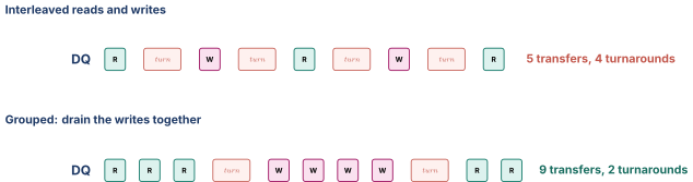
The DQ pins are bidirectional. On a read, the DRAM drives them and the controller's PHY receives. On a write, the controller's PHY drives them and the DRAM receives. Turning that around is not free. The driving end must stop driving and let its output stage go high-impedance, the line must settle, the on-die termination configuration usually has to change at both ends, and only then may the other end begin driving. Overlap the two and you have two drivers fighting on a transmission line, which is contention, reflections, and potentially damage.
JEDEC therefore specifies turnaround minimums. and gate write-to-read, measured from the end of the write data burst, and are around 2.5 ns and 7.5 ns respectively for DDR4. Read-to-write is derived from CL, CWL, and the burst length rather than being a single named parameter, and it typically costs a comparable bubble.
The mechanism that exploits this is write draining, and its shape is the same in every controller.
Writes are posted. Nobody is waiting for a write to complete, so the controller accepts them into a write buffer and acknowledges immediately. It then serves reads preferentially, because reads have a core stalled behind them. When the write buffer reaches a high watermark the controller switches into drain mode, pays one turnaround, drains writes back to back until the buffer falls to a low watermark, pays one turnaround back, and returns to serving reads.
The two watermarks are the design knobs and they trade cleanly. A high watermark set too low means the controller drains often and pays many turnarounds. Set too high, it means that when a drain finally happens it is long, and any read that arrives during the drain sees a very large latency spike. This is the single largest source of memory-latency tail on a well-built system, and being able to say that, and to say that you would size the watermarks against the read-latency tail rather than against average bandwidth, is a strong answer.
Two refinements are worth knowing. The drain can be interrupted by a read to an address that the write buffer holds, which must be forwarded from the buffer rather than fetched, exactly like store-to-load forwarding in Load Store and Memory Ordering. And a controller can bias the drain toward writes that hit already-open rows, so that the drain itself is efficient rather than merely long.
6.5 Starvation, and the thing FR-FCFS gets wrong
FR-FCFS maximises throughput and it is unfair by construction, which is not a subtle side effect but a direct consequence of rule 1.
Consider two clients sharing one bank. Client S is a streaming engine with excellent row locality, so almost all of its queued requests are row hits. Client L is a latency-sensitive core issuing occasional scattered requests, so almost none of its requests are row hits. Under FR-FCFS, every one of S's hits outranks every one of L's misses, forever, as long as S keeps the queue supplied. L is starved not because it is slower but because it is less regular, and the more the memory system is optimised for throughput the worse L does. The academic literature on this is extensive and public, running from stall-time-fair scheduling through blacklisting schedulers, and the finding is consistent: naive FR-FCFS on a multi-core machine can slow a well-behaved application down by a large factor because of a badly-behaved neighbour.
The fixes are all versions of bounding the damage rather than abandoning the policy.
An age cap. Every request carries an age counter. Past a threshold it is promoted to the highest priority regardless of hit status, which converts unbounded starvation into a bounded worst case. Choosing the threshold is a direct latency-versus-throughput dial.
A batch bound. Cap how many consecutive row hits one open row may serve before the row must yield, which limits the length of any one client's run.
Per-client quotas. Track bandwidth consumed per client over a window and de-prioritise a client that is over its share. This is the mechanism that generalises into the quality-of-service machinery of Part 8.
Per-thread request batching. Group requests into batches by arrival epoch and complete a batch before starting the next, so no request can be passed over indefinitely. This is the idea behind several published fair schedulers.
The framing to have ready: FR-FCFS is the right default and the wrong policy to ship unmodified, because it optimises a metric, aggregate throughput, that nobody actually experiences. What users experience is the latency of the slowest thing they are waiting on.
07.Part 7, refresh
7.1 What a REFRESH command actually does
A refresh is not a special operation. It is an ACTIVATE followed by a PRECHARGE with the data thrown away.
That is the whole mechanism, and it falls straight out of Part 1.2. Activating a row sense-amplifies every cell on it and then restores every cell to a full rail. Restoring is exactly what a leaking capacitor needs. So refreshing a row means opening it and closing it again, and the fact that DRAM must be refreshed is not an extra circuit, it is a consequence of the read being destructive and the restore being the fix.
What the REFRESH command adds is bookkeeping. The device keeps an internal row counter, so the controller does not have to name a row. It issues REF, the device refreshes whatever block of rows the counter points at in every bank, and increments. On the 8 Gb DDR4 part worked in Part 1.1 that block is eight rows in each bank. The controller's only job is to issue REF often enough.
Two preconditions follow and both are load-bearing. All banks addressed by the refresh must be precharged first, because you cannot activate a refresh row in a bank that already has a different row open. And the device accepts no other command for afterwards, because it is internally busy activating and restoring in every bank at once.
7.2 The bandwidth cost, computed
The device is unavailable for out of every , so the fraction of time lost is simply the ratio.
For a 16 Gb DDR4 device at normal temperature:
For the same device above 85 °C, where halves to 3.9 µs:
For a 16 Gb DDR5 device, where is around 295 ns and is 3.9 µs:
Three observations, and the second and third are the ones worth having.
Seven percent is a lot. It is a permanent, unavoidable tax on a resource that is already the bottleneck, and on a hot part it doubles. Any candidate who says refresh is negligible has not done the division.
DDR5 did not fix it. It halved and it halved , and 7.6 percent is not better than 7.0 percent. What DDR5 changed is the granularity, which affects the latency spike rather than the average, and that turns out to matter more than the average does.
It is getting worse with density, not better. An 8 Gb DDR4 device has around 350 ns, so its tax is percent. Going from 8 Gb to 16 Gb took it from 4.5 to 7.0 percent. The reason is structural: grows roughly with the number of rows to restore, while the retention window is a property of the cell and does not grow. Extrapolate and the trend is uncomfortable, which is why in-DRAM refresh management and finer-grained schemes are an active area of published research.
7.3 All-bank, per-bank, and same-bank
All-bank refresh, REFab, is the classic scheme. Every bank refreshes together, so every bank must be precharged first and the whole device is dead for . Its virtue is simplicity: one command, one counter, nothing to track.
Per-bank refresh, REFpb, exists in LPDDR. The controller names one bank, that bank refreshes, and the other banks continue serving traffic. The interval is correspondingly shorter, for an 8-bank grouping, so you issue eight times as many refresh commands each covering an eighth as much work. The total array work is identical. What changed is that the device is never fully unavailable.
Same-bank refresh, REFsb, is DDR5's version of the idea. It refreshes one bank in each bank group simultaneously, so for a device with 32 banks in 8 groups it refreshes 8 banks and leaves 24 available. Public descriptions tie it to fine-granularity refresh mode, so a controller using it issues refreshes about twice as often as the baseline all-bank interval, roughly every 1.95 µs on a 16 Gb part against 3.9 µs, and each one occupies the device for far less time: published figures put the same-bank refresh at around 130 ns against the 295 ns of an all-bank refresh on that part.
The trade-off is real and worth stating rather than presenting per-bank as strictly better. Per-bank and same-bank refresh have worse aggregate efficiency, because each command carries fixed overhead that is now amortised over less work, so total time spent refreshing goes up somewhat. What they buy is that the maximum stall any single request can suffer from refresh drops from , which can be 550 ns and is enormous compared to a 40 ns access, to something several times smaller. You trade a little average bandwidth for a much better tail, and on a system with a real-time client that is unambiguously the right trade. On a throughput server it is arguable.
7.4 Postponement, pull-in, and the scheduling freedom that exists
The word average in "REFRESH commands at an average interval of " is the most useful word in the refresh specification, because it means the controller does not have to issue refreshes on a metronome.
JEDEC permits the controller to postpone up to eight refreshes and to pull in up to eight. Concretely, the controller maintains a signed credit counter that increments every and decrements on every REF issued, and the standard permits that counter to range roughly over . The obligation is only that the running average is met and that the counter never leaves the window.
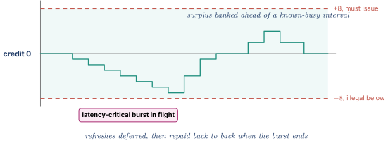
The scheduling policies that fall out of that freedom are exactly what distinguishes a good controller.
Defer under load. If the command queue is deep and a refresh is not yet urgent, hold it. Issuing a refresh in the middle of a well-scheduled burst of row hits costs the full plus the loss of every open row, since every bank must precharge first.
Issue opportunistically when idle. If the queue is empty, spend the credit now. A refresh issued into idle time is genuinely free.
Watch the deadline. When the credit approaches the limit the refresh must be promoted above everything, because missing it is not a performance bug, it is data loss.
Account for the row-buffer destruction. A refresh forces every bank to precharge, so it does not only cost , it also throws away every open row and converts the next access to each bank into a miss. That second cost is frequently larger than the first and it is the part most people forget. It is also the strongest argument for per-bank refresh, which only destroys one bank's open row at a time.
Two more mechanisms are worth naming because they surface in mobile and automotive parts. Temperature-compensated self refresh lets the device use its own on-die temperature sensor to slow its self-refresh rate when it is cold, since retention improves at low temperature, which saves real standby power. And DDR5 adds error check and scrub, ECS, an in-device operation that reads, corrects with on-die ECC, and writes back, addressing the error-accumulation problem that Part 7.9 of SRAM Arrays and ECC describes for caches.
08.Part 8, quality of service, and many clients on one controller
8.1 Three clients with genuinely different needs
An SoC memory controller does not serve a CPU. It serves everything, and these roles for this kind of role phrase the problem as clients with varying but simultaneous needs, which is an exact description of the difficulty. Make it concrete with three archetypes.
The display engine is real time. It reads a frame buffer on a fixed schedule dictated by the panel, not by software. Its bandwidth is modest and utterly predictable. Its requirement is a hard deadline: if the pixel data is not in the display FIFO when the panel wants it, the user sees a visible glitch on a shipping product. There is no such thing as a slightly late scanline.
The CPU is latency sensitive. Its bandwidth demand is small and bursty. Every one of its requests may have an out-of-order window's worth of instructions stalled behind it, per Out of Order Execution, so the marginal value of ten nanoseconds saved is enormous. It cannot tell you in advance what it will need.
The GPU or neural engine is bandwidth hungry and latency tolerant. It issues enormous numbers of concurrent requests, has hundreds or thousands of threads to switch among while waiting, and cares only about aggregate throughput over a frame or an inference. It will happily consume every byte per second the memory system can produce.
Those three want opposite things from the scheduler, and the conflicts are specific rather than vague. The GPU's request flood, scheduled under FR-FCFS, starves the CPU by the exact mechanism of Part 6.5. The display's deadline is violated by any long unbroken run of anybody else's traffic. And the CPU's latency is destroyed by a write drain that happens to start at the wrong moment.
8.2 Why the display case is a tail problem, worked
Do the arithmetic, because it reframes the problem correctly and most people get the framing wrong.
A 4K display at 3840 by 2160 pixels, 4 bytes per pixel, at 60 Hz, needs
for one layer. Against a DDR4-3200 channel's 25.6 GB/s that is under 8 percent of peak. On an average-bandwidth basis the display is a rounding error.
Now look at the deadline. The display engine buffers some number of lines on-chip. Take a 32 KB line buffer as an illustrative figure. It drains at 2.0 GB/s, so from full it empties in
and refilling it at full channel rate takes only 1.28 µs. So there is enormous slack in aggregate and a hard wall at 16.4 µs. What kills a display is not that it needs bandwidth, it is that it needs some bandwidth within every 16 microsecond window, without exception, forever. One unlucky interval where the GPU has the machine and a 550 ns refresh lands on top of a long write drain is not a problem. Ten thousand of them in a row is a visible artefact.
State the conclusion in one line, because it is the framing that separates a designer from a spec reader. Memory-side quality of service is a tail-latency problem disguised as a bandwidth problem. The average is fine. The whole design exists to bound the worst case.
8.3 The mechanisms, and what each one actually guarantees
Traffic classes. Requests carry a class on the fabric, typically a small field on the AXI or CHI channel. Three or four classes are usual: real-time, low-latency, best-effort, and sometimes a low-priority background class for things like scrubbing. Everything downstream keys off this field, so it must be assigned correctly at the master and must survive the fabric intact, which is an integration contract issue of the kind in SoC Integration and Interfaces.
Separate queues per class. One shared transaction queue lets a flood of best-effort requests physically occupy every entry, at which point no scheduling policy can help because the high-priority request cannot even be accepted. Either give each class its own queue or reserve entries per class. Head-of-line blocking in the queue defeats every downstream priority scheme, and saying that is a good signal because it is the failure people discover in silicon rather than in review.
Urgency escalation from a watermark. The display engine exports a signal, often literally called urgency or an equivalent, derived from its own FIFO occupancy. At normal occupancy it requests at ordinary priority. Below a warning watermark it escalates. Below a panic watermark it goes to absolute top priority and the memory controller drops everything else. This is the mechanism that makes the 16 µs slack usable: most of the time the display is just another client, and only when it is genuinely in danger does it get to be selfish. It is a closed-loop control problem and the watermarks are its tuning constants.
Bandwidth regulators, or token buckets. Each client gets a token bucket refilled at its allocated rate with a bounded depth. Requests spend tokens. A client with no tokens drops to best-effort priority. This gives every client a guaranteed minimum rate and lets it exceed that only when nobody else wants the bandwidth, which is exactly the property you want. It also bounds how badly one client can hurt another, which is what makes system-level timing analysis possible at all.
Latency targets rather than priorities. A more modern framing gives each class a target latency and has the arbiter promote requests as they approach it, which is more robust than static priority because it degrades gracefully. Static priority has a failure mode where a high-priority client that becomes unexpectedly busy causes complete collapse of everything below it, with no warning.
Deadline-aware refresh and drain. The refresh credit of Part 7.4 and the write watermarks of Part 6.4 should both be aware of real-time urgency. A controller that starts a 550 ns refresh or a long write drain immediately after the display escalates has defeated its own quality-of-service scheme with its own housekeeping.
The honest thing to add, because a good interviewer will get there, is that none of these mechanisms is a proof. They bound the worst case only under assumptions about the other clients' behaviour, and those assumptions are checked by simulation with worst-case traffic generators rather than by formal argument, except in genuinely safety-critical designs where a formal worst-case-execution-time analysis is done and is very conservative. Knowing where the guarantee comes from, and that it is empirical, is a more mature answer than claiming the mechanism guarantees anything.
09.Part 9, LPDDR, and what mobile changes
9.1 The electrical and topological differences
LPDDR is not DDR with the voltage turned down. The differences are structural and they all follow from one design goal: a soldered-down, short, point-to-point channel in a device that is asleep most of the time.
No DIMM, no sockets, no fly-by daisy chain. LPDDR is soldered or package-on-package next to the SoC, so the channel is short and the loading is known at design time. That removes the signal-integrity problems that drove several DDR features, and it means shorter flight times and less training complexity in some respects.
Narrower channels, more of them. A DDR5 subchannel is 32 bits. An LPDDR5 channel is 16 bits, and mobile SoCs instantiate many of them. Do not take that as a bare fact, run the same cache-line arithmetic as Part 2.3 on it and the consequence falls out. Sixteen bits at a burst of sixteen is bits, which is 32 bytes, half a cache line. So where DDR5 tuned its subchannel width and burst length to land exactly on 64 bytes, LPDDR5's natural granule is finer, and a 64-byte line arrives either as two BL16 bursts or as the single BL32 burst LPDDR5 also defines. That is a deliberate choice rather than a shortfall: a 32-byte granule suits scattered, fine-grained phone traffic better than it suits a server streaming lines, and it means an LPDDR controller sees a request mix, and makes a coalescing decision, that a DDR controller never has to. Narrow channels are also better for power, because you can idle a channel you are not using, and better for concurrency, because more channels means more independent command buses.
Lower voltages and different termination. LPDDR runs at lower supply and I/O voltages than the DDR line at comparable generations, and it uses different termination strategies because the channel is short enough not to need the same on-die termination that a multi-drop DIMM channel requires. Fewer terminated lines is a direct, permanent power saving.
A different command encoding. LPDDR uses a narrow multi-cycle command/address bus rather than a wide single-cycle one, trading command bandwidth for pin count and power. That has a real consequence for the controller: commands take multiple clocks to transmit, so the arbiter's issue slot model is not one command per cycle and the scheduling logic has to account for command-bus occupancy explicitly.
A separate write clock. LPDDR5 introduces WCK, a fast write clock separate from the command clock CK, which runs at a lower rate. This decouples the command bus rate from the data rate and lets the command path stay slow and low-power while the data path goes fast. It also adds a WCK synchronisation sequence the controller must run before a burst, which is more state machine work and appears explicitly in the DFI signals of Part 10.
9.2 The power states, and the one distinction that matters
The state machine is where mobile diverges most, and there is one boundary in it that is the whole point.
Active. A row is open somewhere, commands are flowing, clock is running.
Power-down. The device stops its internal clock receivers and much of its command path but retains all state including any open row. Exit is fast, in the region of a few clock cycles to tens of nanoseconds. This is the state to enter when the controller expects idle for hundreds of nanoseconds, and it is the DRAM analogue of clock gating.
Self-refresh. The controller precharges everything, tells the device to enter self-refresh, and then may stop the clock entirely and power down its own PHY. The device runs its own oscillator and refreshes itself, using its own temperature sensor to pick a rate under temperature-compensated self refresh. Contents are retained. Exit takes appreciably longer, on the order of hundreds of nanoseconds to microseconds, because the clock has to restart, the DLL has to relock, and depending on how deep the state was, some retraining may be needed.
Deep sleep or deep power-down. Internal voltage generators not needed for retention are shut off. LPDDR5 defines a deep sleep mode of this kind and public material claims a substantial further reduction in self-refresh power over ordinary self-refresh, though the specific percentages quoted in vendor material vary and I would treat any single figure with caution. In the deepest variant, deep power-down, the contents are not retained at all and the memory must be re-initialised and reloaded on exit.
That last line is the distinction to be exact about, because it is a favourite question. Self-refresh retains, deep power-down does not. Everything else about the two states is a matter of degree, and that one thing is a difference in kind. It determines whether exiting the state is a hardware sequence measured in microseconds or a software event measured in milliseconds that has to reload from storage.
The break-even reasoning is identical in structure to the power-gating arithmetic in Part 6.3 of Power Fundamentals and Clock Gating, and it is worth doing rather than gesturing at. Each state costs a fixed energy to enter and leave, covering the PHY power-down and power-up, the clock restart, the DLL relock and any retraining, and each saves a standing power for as long as it lasts. The state pays only when the idle window exceeds
Put illustrative numbers through it, in the same spirit as the line-buffer figure in 8.2 and not as datasheet values, since the real ones come from the part's IDD table and the PHY's own numbers. If the self-refresh entry and exit sequence costs 2 µJ and the state saves 20 mW of standing power, the break-even is 100 µs. A 10 µs gap is then decisively power-down territory and a 10 ms gap is decisively self-refresh, and the interesting engineering is entirely in the band between them. That is the same shape as the 2 µs power-gating break-even in note 17, arrived at from different physics, which is exactly why the reasoning transfers. The rule the controller runs is therefore one line: estimate the coming idle, and pick the deepest state whose break-even time is shorter than that estimate. The estimate is imperfect, which is why real controllers use staged timeouts: enter power-down after a short idle, promote to self-refresh after a longer one, and let software or a system power manager request the deepest states explicitly because only software knows the machine is about to be idle for a second.
9.3 What the controller has to do differently
Frequency set points. Mobile SoCs scale memory frequency aggressively with load, which is the DVFS story of DVFS Droop and Thermal applied to the memory system. Every timing parameter in Part 4 has to be recomputed at each frequency, since the form changes which term binds. LPDDR defines frequency set points, banks of mode-register settings that can be pre-programmed so that a frequency change is a switch between prepared configurations rather than a full reprogram-and-retrain. The controller has to sequence that change safely: quiesce traffic, switch, resynchronise, resume. It is a multi-step protocol with a wrong answer at every step, and it is exactly the kind of state machine a logic design role would own.
Aggressive idle detection. On a phone the memory system is idle far more than it is busy, so the low-power state machine runs constantly rather than occasionally. That makes the entry and exit sequences performance-critical in a way they are not on a server.
Inline rather than sideband ECC. LPDDR has no spare devices for check bits, which is Part 11.2.
Per-bank refresh as the default. With a real-time display client and a hard deadline, the tail argument of Part 7.3 is decisive rather than arguable.
10.Part 10, DFI, and the controller / PHY split
10.1 Why the split exists at all
Everything up to here has been digital. The controller decodes addresses, runs counters, arbitrates, and issues commands, and every one of those is synthesisable RTL that a synthesis tool will happily map onto standard cells in any process.
Then the commands have to become voltages on package pins running at several gigatransfers per second into a channel with reflections, crosstalk, and a temperature-dependent flight time. That is not digital logic. It needs per-bit programmable delay lines with picosecond resolution, phase-locked or delay-locked loops, calibrated output drivers, on-die termination whose impedance is trimmed against a precision resistor, receivers with trainable reference voltages, and clock generation that can be reconfigured on the fly. Every one of those is a custom analogue or mixed-signal circuit, hand-designed for one specific process node, delivered as a hard macro with a fixed floorplan footprint and its own power rails.
So a DDR subsystem is always two very different objects: a memory controller, portable synthesisable RTL, and a DDR PHY, a process-specific mixed-signal hard macro. They come from different teams, often from different companies, and they are verified by completely different means.
If the interface between them were ad hoc, then every controller would only work with one PHY and every PHY change would force a controller change. DFI, the DDR PHY Interface, exists to make that boundary a standard. It is published by the DFI group at ddr-phy.org, it is not a JEDEC standard, and it is a purely digital synchronous interface: a set of named signals, their widths, their timing relationships, and the protocols built on them. DFI 5.0 is the version aimed at DDR5 and LPDDR5.
The distinction to be exact about, because it is a trap: DFI is not a memory protocol. It carries no DRAM commands in JEDEC's encoding, it defines no DRAM timing, and the DRAM has never heard of it. It is the interface between two blocks on your die. Nothing about DFI appears on any pin that leaves the package.
10.2 What DFI standardises
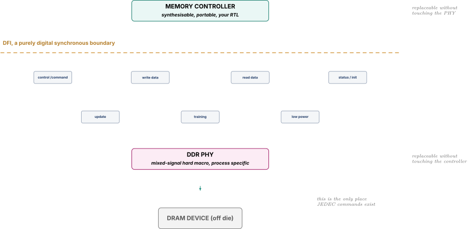
The signal groups are the useful thing to know by name, because they map onto the controller's internal structure almost one to one.
The control interface carries the command and address that the PHY will drive onto the DRAM's pins: the address bus, the bank and bank-group selects, chip select, clock enable, and the command encoding bits, all as ordinary digital signals in the controller's clock domain.
The write data interface carries write payload with an enable and a mask, and the key parameter here is tphy_wrlat, the number of DFI cycles from the controller asserting the write-data enable to the PHY actually launching data on the DQ pins. The controller must know that number to place its write data correctly relative to the WRITE command it already sent.
The read data interface is the mirror. The controller asserts a read-data enable to tell the PHY when to expect returning data, the PHY captures it and returns it with a valid signal after a further latency. The read-latency parameter and the enable timing are the pieces the controller must configure correctly, and getting them wrong produces data that is present but shifted, which is a memorable bring-up failure.
The update interface handles periodic maintenance where either side may need to pause traffic. dfi_ctrlupd_req is the controller telling the PHY it may perform an update now. dfi_phyupd_req is the PHY asking the controller for a window because it needs to retrain or recalibrate. Both are handshakes with an acknowledge, and the PHY-initiated direction matters because delay lines drift with temperature and the PHY is the only thing that knows.
The status and initialisation interface carries reset and initialisation start and complete, plus the frequency ratio configuration.
The low-power interface is the handshake by which the controller tells the PHY to enter or leave its own low-power states, with dfi_lp_ctrl_req and dfi_lp_data_req and their acknowledges, coordinated with the DRAM power states of Part 9.2.
The training interface is how the controller and PHY coordinate the calibration of 10.3. Its shape changed substantially in DFI 5.0, which moved to a PHY-independent training mode in which the PHY trains the memory interface itself without the controller participating in the sequence. The controller's job becomes granting the PHY a window and waiting, which is a considerably simpler contract and removes a large amount of protocol-specific knowledge from the controller.
DFI 5.0 also adds LPDDR5-specific machinery, including signals for frequency set points and for the WCK write clock of Part 9.1, with dfi_wck_en and dfi_wck_toggle communicating the write clock's state.
10.3 Training, and why an interface has to be measured before it works
This is the part that surprises people who have only done fully synchronous digital design, and it is worth stating starkly. A DDR interface does not work when you power it on. It has to be measured and adjusted before the first useful transaction, every time, and then re-measured periodically forever.
The reason is that the timing relationships depend on things nobody knew at design time: the actual board trace lengths, the actual package parasitics, this particular die's process corner, the current supply voltage, and the current temperature. At 3200 MT/s a data eye is 312 ps wide before you subtract jitter and skew, and the total uncertainty across those sources exceeds it. So the interface characterises itself.
Command and address training aligns the command bus to the clock at the DRAM, since a command sampled on the wrong edge is a random command.
Write leveling is the one worth understanding in detail because it is the clearest example of the principle. On a DIMM, the clock and command signals are routed fly-by, daisy-chained from one DRAM to the next, which is excellent for signal integrity because each device presents one small stub instead of a big multi-drop star. The cost is that the clock arrives at the last device meaningfully later than at the first. Data and its strobe DQS, meanwhile, are routed point to point, so if the controller launched every byte lane's DQS simultaneously, each device would see a different DQS-to-clock relationship and only one of them could be right. JEDEC's fix is elegant: put the DRAM into a mode where it samples the clock using DQS as the sampling edge and reports the result back on DQ. The controller sweeps the delay on that byte lane's DQS and watches the reported bit flip from 0 to 1, which is the moment DQS crossed the clock edge. That transition point is the alignment, and the controller programs the PHY's per-lane delay accordingly. The relevant JEDEC parameter is , the tolerance on the DQS-to-clock relationship at the device, which is specified as a fraction of a clock period, commonly .
Read gate training, also called DQS gate training, solves the opposite problem. On a read the DRAM sends DQS back along with the data, but DQS is not free running: it is tri-stated between bursts and floats to an indeterminate level. The PHY therefore has to open a gate at exactly the right moment, enabling its DQS receiver just before the preamble arrives and closing it after the postamble. Too early and it captures noise on a floating line, which looks like phantom data. Too late and it misses the preamble and the whole burst shifts. The correct gate position depends on the round-trip flight time, which is a board property nobody knew at tapeout, so it has to be measured by reading known patterns and sweeping the gate position.
Read and write DQ centring, sometimes called eye training, adjusts the per-bit delay on each DQ line so that the sampling point sits in the middle of that bit's eye rather than at its edge. It is done per bit because trace lengths and driver strengths differ bit to bit.
Reference voltage training sweeps the internal used to slice the incoming signal, since the optimal slicing level is not exactly mid-rail once you account for the actual channel.
ZQ calibration is the odd one out because it is not about timing at all. A precision external resistor, conventionally 240 Ω and referred to as RZQ, gives the device an absolute impedance reference. The device calibrates its output driver impedance and its on-die termination values against it. This must be redone periodically, because the transistors implementing the driver and the termination drift substantially with temperature and voltage, and an impedance mismatch produces reflections that close the eye. The commands are ZQCL for a long initial calibration and ZQCS for a short periodic one, and issuing them is the controller's job.
Two consequences of all of this are worth stating because they change how you think about the block.
Training is periodic, not one-off. Temperature drifts during operation, so the delays drift, so the interface must be retrained or incrementally recalibrated on an ongoing basis. That is what the dfi_phyupd_req handshake is for, and it means the controller must be able to quiesce traffic on demand at any moment.
Training is where bring-up fails. When a new board does not boot, the memory interface is the usual suspect and the training log is the first thing anyone reads. Being able to say that, and to name write leveling and gate training as the two that fail most visibly, is a credible thing to know without claiming to have owned a PHY.
10.4 What the split means for the controller RTL
Three concrete consequences, and all three are logic-design work rather than analogue work, which is exactly why the DDR-PHY knowledge is listed as a plus rather than a requirement on a controller role description.
The frequency ratio. The controller usually cannot run at the memory clock, because a 1.6 GHz clock through a wide arbiter will not close timing in a reasonable power budget. DFI therefore supports frequency ratios of 1:1, 1:2, and 1:4, meaning the controller runs at half or a quarter of the memory clock and issues multiple commands per controller cycle. That is why DFI signals come in phase-indexed sets, with a separate copy of the address and command bus per phase. The consequence for the RTL is significant: the arbiter must select two or four commands per cycle rather than one, and it must check the JEDEC timing constraints between the commands within a single cycle as well as across cycles. A pair of activations issued in phases 0 and 1 of the same controller cycle are one memory clock apart, and still applies. That intra-cycle checking is a genuinely tricky piece of logic and is a good thing to have thought about.
Clock domain crossing. The fabric side of the controller runs at the interconnect clock, the DFI side runs at the controller clock derived from the memory clock, and those are asynchronous to each other. So there is a real domain crossing in the middle of the block, carrying wide data in both directions, which means asynchronous FIFOs with gray-coded pointers and multi-flop synchronisers exactly as in Clocking Reset and Domain Crossing. It is also a place where the crossing must survive one side's clock stopping, because self-refresh entry lets the memory clock stop entirely, and a synchroniser whose destination clock has stopped never resolves. That is the deadlock case from Part 4.4 of Power Fundamentals and Clock Gating arriving in a new context, and the wake path has to be built accordingly.
Latency accounting. The controller knows the JEDEC latencies and the PHY adds its own, so every timing calculation in the controller is really a JEDEC parameter plus a configured PHY latency. The read-data enable in particular has to be asserted a configured number of cycles after the READ command, and if that configuration is wrong the data is captured in the wrong window. Those PHY latency values are configuration registers, not constants, and the controller's timing model must be parameterised on them.
11.Part 11, ECC on main memory
11.1 Why main memory needs it, and what the codes are
The coding theory is all in Part 7 of SRAM Arrays and ECC and is not repeated here. What matters is that the standard code for memory is SECDED, an extended Hamming code correcting one error and detecting two, at 8 check bits per 64 data bits for 12.5 percent overhead, and that its limits are exactly the ones that note describes: it is helpless past two errors and will silently miscorrect three.
The reason main memory needs protection at all is a combination of scale and exposure. A single machine may hold hundreds of gigabytes of DRAM cells, each one a leaking capacitor holding tens of femtofarads of charge, exposed to particle strikes, retention failures at the tail of the distribution, and disturbance from neighbouring rows. Multiply any small per-bit rate by bits and you get events per day. And unlike a cache, main memory usually holds the only copy.
What changed recently is that the raw error rate inside the DRAM die rose to the point where the devices could not ship without internal correction. That is the origin of on-die ECC, and it is the fact that reorganised this whole topic.
11.2 The four schemes, and what each one covers
The confusion in this area is almost entirely about coverage, meaning which part of the path a given scheme protects, so organise the answer around that rather than around the codes.
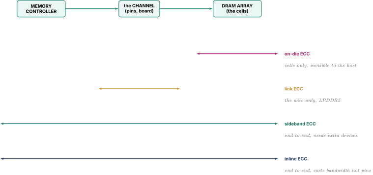
Sideband ECC is what "ECC memory" traditionally means. The rank is widened, so a 64-bit channel becomes 72 bits by adding an extra x8 device, and those extra eight bits per beat carry the check bits. The controller generates them on write and checks them on read. Coverage is end to end, from the controller's own logic all the way through the array and back, because the check bits travel with the data over the same wires at the same time. The cost is one extra device per rank, which is 12.5 percent of capacity, cost, and pin count, plus the board and package width to route it.
Inline ECC stores the check bits in the same DRAM devices as the data, in a region of the address space reserved by the controller and hidden from software. No extra pins and no extra devices. Coverage is also end to end. The cost moves from pins to bandwidth and latency, because the check bits are additional data that must be fetched, and unless the layout is arranged carefully they may require a second access to a different address. Good implementations place a granule's check bits so they can be fetched in the same burst or the same open row, which limits the penalty. Naive ones can cost far more than 12.5 percent. Inline ECC is the scheme used where widening the bus is impossible, which is exactly the LPDDR case and also FPGA and automotive designs.
On-die ECC lives entirely inside the DRAM die and is mandated in DDR5. Public descriptions put it at roughly 8 check bits per 128 data bits, correcting single-bit errors within the array before data leaves the device. Its coverage stops at the DRAM's own pins. It exists because raw cell error rates at current densities are too high to ship without it, and the crucial thing to understand is that it is a yield and reliability measure for the DRAM vendor, not a data-integrity feature for the system. It does not protect the link, and in its base form it does not report corrected errors to the host in a way system software can act on. DDR5 adds error check and scrub to address the accumulation problem, but the fundamental limitation stands.
Link ECC is an LPDDR5 feature protecting the channel only. On a write the controller computes check bits and sends them alongside the data on designated bits. The DRAM checks and corrects. On a read the direction reverses. It exists because at LPDDR5 data rates the dominant error source on a mobile part is signalling on the wire, not retention in the cell, and it is much cheaper to protect the wire than to widen the bus.
11.3 The sentence that ties it together
Say this and you have answered the whole family of questions at once. On-die ECC protects the cells, link ECC protects the wire, and neither of them protects the system, because a system-level guarantee requires that the check bits the controller generated are the check bits the controller checks. Only sideband and inline ECC have that property, because only they carry the controller's own code all the way to the array and back. On-die and link ECC each cover one segment and hand off in the middle, and a fault in the handoff is invisible to both.
The practical consequence, which is the standard follow-up: a DDR5 system without ECC DIMMs is not an ECC system, even though every DDR5 chip on it contains ECC. The industry consensus reflected in vendor documentation is that on-die and sideband ECC are complementary rather than alternatives, and servers still require ECC DIMMs.
11.4 The controller-side consequences
Four of them, and the first is the one that separates people who have implemented ECC from people who have read about it.
Partial writes force a read-modify-write. If the ECC granule is 64 bits and a client writes 8 of those bits, the controller cannot compute the new check bits, because they depend on all 64. It must read the granule, merge the new bytes, recompute the check bits, and write the whole granule back. That converts a write into a read plus a write, roughly triples its cost, and does so on traffic that looks trivially small to whoever generated it. Every ECC-protected memory system has a story about a driver doing byte writes into a large buffer and destroying memory performance. The mitigations are the data-mask pin where the device supports masked writes, write coalescing in the controller so that adjacent partial writes merge into a full granule before draining, and telling software to write whole lines.
Note the wrinkle that DDR5 introduces here: because on-die ECC has the same problem inside the device, a masked write requires the DRAM itself to do an internal read-modify-write, and the treatment of the data mask changed in DDR5 relative to DDR4. I would check the exact rules for a given device organisation in JESD79-5 rather than assert them, but the direction is clear and the reason is exactly the granule argument above.
ECC sits on the read latency path. Every read must be checked before it can be forwarded, and the syndrome computation plus correction is real logic. The standard technique is the same as in a cache: forward the data speculatively and signal an error a cycle or two later, which trades a small amount of recovery complexity for not adding latency to the common case. That is the same design decision, for the same reason, as the speculative-forward pattern in SRAM Arrays and ECC.
Scrubbing. Errors accumulate. A word with one corrected error is one particle strike away from an uncorrectable double. Patrol scrubbing walks memory in the background at a low rate, reading each location, correcting any single error, and writing it back, so that corrected errors are cleaned up rather than accumulating. It costs a small, tunable fraction of bandwidth and it is the direct analogue of the cache scrubbing argument in SRAM Arrays and ECC. The scrub rate is chosen so that the whole array is covered in well under the expected time between errors in a single word.
Reporting. Corrected errors must be counted and reported, because a rising corrected-error rate on one address is the early warning of a failing device, and replacing it before it produces an uncorrectable error is the entire operational value of ECC. A controller that corrects silently and reports nothing has thrown away half the benefit.
12.Part 12, the interview questions, with answers
Fifteen questions of the kind actually asked for a memory-controller logic-design role, each with a model answer written the way a strong candidate would speak it rather than the way a textbook would write it, the follow-up the interviewer will reach for next, and the trap where there is one. Read the answers out loud. They are calibrated to be spoken in one to three minutes, which is the real constraint.
Q1. Walk me through what happens when a load misses the last-level cache.
Model answer. The miss allocates an MSHR in the last-level cache and the request goes out onto the fabric as a read of one cache line, tagged with an ID so the response can be matched back. It crosses the interconnect to the memory controller, where the first thing that happens is a domain crossing into the controller's clock, then it is accepted into the transaction queue if there is room and if it does not overlap an in-flight write.
The controller then decodes the physical address into channel, rank, bank group, bank, row and column. That mapping is a configuration choice, not a fixed one, and it decides most of what happens next. It looks up that bank's state and gets one of three answers. If the bank already has that row open it just needs a column read. If the bank is idle it needs an activate then a read. If the bank has a different row open it needs a precharge, then an activate, then a read.
Those commands go into a command queue and wait for two things: for the JEDEC timers on that bank to allow them, and for the arbiter to choose them over everything else in flight. At DDR4-3200 the device part of this is roughly fourteen nanoseconds if it hits, twenty-eight if the bank was idle, forty-one if it conflicts. Then the data comes back through the PHY, gets ECC checked, gets reassembled into a line, goes back over the fabric, and fills the cache.
The thing I would emphasise is that the DRAM device is usually the smaller half of the total. On a modern part, idle memory latency measured from the core is somewhere in the sixty to ninety nanosecond region and the device accounts for maybe a third of it. The rest is fabric in both directions, controller queueing, and the fill path. Under load the queueing term can dominate everything else, because a queue near full utilisation has an unbounded wait.
The follow-up. "Where would you spend effort to reduce it?"
Answer by which term you are attacking. If the device term dominates, you attack the row-hit rate, which means the address map and the scheduling policy. If the queueing term dominates, you are bandwidth-limited rather than latency-limited and the answer is more banks in flight, better bank-level parallelism, or more channels. If the fabric term dominates, that is a floorplan and interconnect problem and no scheduler will help. Saying "I would measure which term it is first" is the correct opening and it is not a dodge.
The trap. Answering with CAS latency and stopping. The number people quote from a memory module's sticker is one of three terms in the device latency, which is itself one of three terms in the total. Anyone who answers "CL 22, so 13.75 nanoseconds" has told the interviewer they have never measured a memory system.
Q2. What are a row hit, a row miss, and a row conflict, and what does each cost?
Model answer. A DRAM bank has one row buffer, which is physically the strip of sense amplifiers, and only one row can be in it at a time. A hit means the row I want is already there, so I just issue a read and wait CAS latency. A miss means the bank is idle with nothing open, so I activate and then read, which is plus CL. A conflict means the wrong row is open, so I have to precharge first, which is plus plus CL.
At DDR4-3200 twenty-two-twenty-two-twenty-two those are 13.75, 27.5 and 41.25 nanoseconds, so roughly one, two and three. The distinction between miss and conflict is the one that matters, because a policy that produces lots of misses can easily be better than one that produces lots of conflicts, and that is the entire open-page versus closed-page argument.
The follow-up. "So should you always leave rows open?"
No, and there is a clean break-even. If is the probability that the next access to this bank hits the currently open row, open page costs and closed page costs a flat 27.5. Setting them equal gives . So open page wins if more than half of subsequent accesses hit, and falls as the number of independent streams sharing a bank rises. That is why single-threaded workloads want open page and heavily multi-threaded or GPU workloads often want closed page, and why real controllers use an adaptive policy with a timeout instead of choosing.
The trap. Treating miss and conflict as the same thing, or saying a conflict is "a miss plus a precharge" as if that were a small addition. It is a fifty percent increase over a miss and it is the case every scheduling and mapping decision is trying to avoid.
Q3. Why do bank groups exist, and what do they change in your controller?
Model answer. By DDR4 the external data rate got fast enough that a burst only occupies the bus for a couple of nanoseconds, but the internal path from a bank's sense amplifiers through the column mux and the serialiser to the pins could not recycle that fast. So JEDEC replicated that shared path. A bank group is a set of banks with their own local readout path, and two column accesses to different groups can go back to back at full rate while two to the same group have to be spaced further apart.
That is why almost every parameter has a short and a long form. versus , versus , versus .
Two things change in my controller. The address map should put the bank-group bits low enough that a sequential stream naturally walks across groups, because then the scheduler gets to use the short timings for free. And the arbiter should treat bank group as a tiebreak: given two commands that are both legal and both row hits, prefer the one in a different group from the last command I issued, because that keeps the data bus full.
The follow-up. "What happens if you ignore bank groups entirely?"
You can lose a large fraction of peak bandwidth on a perfectly sequential stream that has no row misses at all, which is the counterintuitive part. Every access hits, the hit rate report looks perfect, and the bus is half idle because every column command is waiting on . That is a failure mode you only find by looking at bus utilisation rather than at hit rate, and it is a good argument for having both counters in your performance monitors.
The trap. Saying bank groups exist "for more parallelism." Banks exist for parallelism. Bank groups exist because the internal readout path could not keep up with the external data rate, and the giveaway that you understand this is being able to explain why the constraint is on column commands to the same group and not just on activations.
Q4. Explain . Why does it exist?
Model answer. says no more than four activate commands in any rolling window, which for DDR4-3200 with a one-kilobyte page is around twenty-one nanoseconds. It applies device-wide regardless of which banks you target.
It exists because of current, not because of anything logical. An activate raises a wordline and fires several thousand sense amplifiers simultaneously, and each of those drives a few hundred femtofarads of bitline from mid-rail to a full rail, all within the same few nanoseconds. That is a large charge moving very fast through the package inductance, and the device's power delivery cannot supply more than a certain number of those per unit time without the internal rails collapsing. So JEDEC caps the rate.
The evidence that this is the right explanation is that is indexed by page size. At DDR4-3200 JEDEC gives thirteen nanoseconds for a half-kilobyte page, twenty-one for one kilobyte and thirty for two. A logical or pipeline constraint would not care how wide the row is. A charge budget has to care, because twice the page is twice the sense amplifiers and twice the charge. I would be careful not to claim it scales linearly, since twenty-one to thirty is not a doubling, but the direction is unambiguous and it is the direction that makes the argument.
The follow-up. "Quantify what it costs you."
Four activates per twenty-one nanoseconds is one every 5.25 nanoseconds. Under fully random access each activation yields exactly one 64-byte column read, so that is 64 bytes per 5.25 nanoseconds, about 12.2 gigabytes per second, against a channel peak of 25.6. So alone caps random-access bandwidth at roughly forty-eight percent of peak before you count refresh or turnaround or anything else. And that agrees with the other way of computing it: you need a column access every 2.5 nanoseconds to saturate the bus, and is the same forty-eight percent.
The design conclusion is that adding banks past a point buys nothing under random access, because binds before the bank count does. What buys something is more column accesses per activation, which is locality, which is the address map.
The trap. Describing as a bank-conflict or array constraint. It is explicitly about power delivery, and it is one of the few places where a physical supply constraint appears directly in a digital protocol specification. Getting that right is a strong signal.
Q5. Design the address mapping for a memory controller.
Model answer. First I would ask what the traffic looks like, because there is no universally best map and any answer that does not depend on the workload is wrong. But the default shape I would start from, from the bottom up, is: byte offset within the line, then column bits, then bank and bank-group bits, then row bits, then rank, then channel at the top or interleaved at a coarse granularity.
The reasoning is that a sequential stream should walk columns of one open row first, which gives me hits. When it runs off the end of a row it should land in a different bank, so that the next activation overlaps with what is still in flight rather than serialising behind it. And bank bits must never be at the top, because then an entire contiguous region lives in one bank and every stream in it serialises.
Then I would add an XOR. Real address streams are full of power-of-two strides, page-aligned buffers, matrix rows, per-thread stacks. Any of those can put two hot streams into the same bank with a plain field split. Folding a few high-order bits into the bank index with an XOR scatters them for a handful of gates.
Let me make it concrete with small numbers. Take four banks, eight rows, eight columns of 64 bytes, so sixteen kilobytes and fourteen address bits. Two clients stream sequentially, one from address zero and one from address 4096. With a plain row-bank-column split, address 0 is bank 0 row 0 and address 4096 is bank 0 row 2, so the two streams fight over one bank and every access after the first is a row conflict. Sixteen conflicts at 45.75 nanoseconds each is about 730 nanoseconds for a kilobyte. If I XOR two row bits into the bank index, the second stream moves to bank 2, both streams get one activation and seven hits, and the same traffic takes something like seventy nanoseconds. An order of magnitude, on the same silicon, from rewiring the bank decoder.
The follow-up. "How would you actually choose one on a real design?"
Make it a configuration register, collect traces from the real workloads, and simulate candidate maps against them. That is what commercial controllers do, and it is not a cop-out, it is the only honest method, because the answer is a property of the software rather than of the hardware.
The trap. Answering with one fixed map and defending it. The interviewer is checking whether you understand that this is workload dependent. The second trap is forgetting the debug cost of the XOR: once you fold bits, an engineer can no longer look at a physical address and know which bank it is in, which makes lab debug and post-silicon triage harder, and a good answer mentions that you would keep a bypass mode.
Q6. Implement FR-FCFS. What does the RTL look like?
Model answer. The policy is two rules. Among commands that are legal right now, prefer a row hit. Among equally preferred, take the oldest. The word "legal" is carrying most of the weight, because legality is the timer state, so really it is a three-level filter: legal, then hit, then age.
Structurally I have a queue of entries, each holding the decoded bank, row, column, direction, age, and a registered ready bit. The ready bit comes from the per-bank timing tracker, which is a set of down-counters per bank plus the device-wide ones for and a four-deep timestamp structure for . Ready is registered, not computed in the selection cycle, because I cannot afford to evaluate timers and then select in the same cycle.
The selection itself is where the timing problem is. A flat sixty-four-way priority pick with an age comparison will not close at a memory-derived clock. So I would do it in two levels: pick the best candidate within each bank, which is a small select over a few entries, then pick among the per-bank winners, which is a select over the bank count. And I would pipeline it, selecting one cycle and issuing the next, accepting that the state I selected against is one cycle stale, which means I need a suppression path for the case where the winner became illegal in between. Losing an occasional issue slot is far cheaper than dropping the clock.
I would also approximate the age rather than comparing full counters. Two or three bits of age bucket, or a round-robin pointer with a starvation override, gets nearly all the benefit for a fraction of the logic.
The follow-up. "How do you stop it starving somebody?"
FR-FCFS is unfair by construction, and the mechanism is specific: a client with excellent row locality produces a continuous supply of hits, and every one of those outranks every miss from a client with poor locality, forever. So the latency-sensitive client is starved not because it is slow but because it is irregular.
The fix I would implement first is an age cap: every request carries an age, and past a threshold it is promoted above hit status. That converts unbounded starvation into a bounded worst case and the threshold is a direct latency-versus-throughput dial. Beyond that, a cap on consecutive hits to one open row, and per-client bandwidth accounting, which is where this turns into the quality-of-service story.
The trap. Describing the policy and stopping. The policy is in every textbook. The interviewer for a logic design role wants the datapath, the pipelining, and the timing closure story, and specifically wants to hear that you know a wide one-cycle priority select over a deep queue is the thing that will not close.
Q7. Open page or closed page?
Model answer. Neither, in a shipping design, but the analysis is clean. If is the probability the next access to a bank hits its open row, open page costs and closed page costs a flat 27.5, and they cross at . So the question reduces to whether more than half of the next accesses hit, and the driver of is not the workload's locality in isolation, it is the number of independent streams sharing a bank, because each one keeps evicting the others.
Single-threaded sequential code has well above 0.9 and wants open page. A GPU with thousands of concurrent threads destroys locality by concurrency alone and often wants closed page. Many-core servers sit in between and it depends on the mix.
In practice I would implement adaptive open page: leave the row open but start a timer, and precharge if nothing hits within the window. That captures most of the open-page benefit while bounding the conflict exposure, and the timer becomes a tunable. I would also use the auto-precharge bit in the read and write commands rather than issuing a separate precharge when I know I want closed-page behaviour, because that saves a command-bus slot.
The follow-up. "How would you make the policy adaptive at runtime rather than by configuration?"
Count hits and conflicts per bank over a window and switch policy per bank when the ratio crosses a threshold, with hysteresis so it does not oscillate. There are published predictors that do this at finer granularity, keyed on the requesting client or on the program counter that generated the access. The thing to be careful about is that any adaptive scheme has a warm-up cost and a mis-prediction cost, so a simple timeout that is roughly right is often better than a clever predictor that is occasionally very wrong.
The trap. Answering absolutely in either direction. Both answers are right for some system, and the interviewer is checking whether you know what the deciding variable is.
Q8. Why do writes hurt, and what do you do about it?
Model answer. Three separate reasons and they compound.
First, the data bus is bidirectional, so every switch between reading and writing costs a turnaround bubble where the driving end goes high-impedance, the line settles, and termination reconfigures. JEDEC gives that as in one direction and it comes out of CL, CWL and the burst length in the other. Nothing is transferred during it.
Second, a write finishes in the array rather than at the pins. runs from the end of the write data burst to when the bank may be precharged, because the sense amplifier still has to charge the cell capacitor through the access transistor. So a write occupies the bank long after the data has gone by, and that occupancy is invisible if you only look at bus utilisation.
Third, with ECC, a partial write forces a read-modify-write, because the check bits depend on the whole granule.
What I do about it is buffer and drain. Writes are posted so nobody is waiting on them. I accept them into a write buffer, acknowledge immediately, and serve reads preferentially because reads have a core stalled behind them. When the write buffer hits a high watermark I switch to drain mode, pay one turnaround, drain back to back until I reach a low watermark, pay one turnaround back, and return to reads. That amortises one turnaround over many transfers instead of one per transfer.
The follow-up. "How do you pick the watermarks?"
Against the read-latency tail, not against average bandwidth. Too low a high watermark means you drain often and pay many turnarounds. Too high means that when a drain finally happens it is long, and any read arriving during it sees an enormous latency spike. This is usually the single largest contributor to memory latency tail on a well-built system, so I would size it by measuring the read latency distribution's high percentiles rather than the mean. I would also allow the drain to be interrupted for a high-priority read, and forward from the write buffer when a read hits an address the buffer holds.
The trap. Thinking about write latency. Nobody is waiting for a write. The cost of writes is entirely what they do to reads, and framing the answer that way immediately signals that you have thought about it.
Q9. How much bandwidth does refresh cost, and what would you do about it?
Model answer. It is the ratio of to , and both come from physics rather than convention. is the retention window divided by the 8192 refresh commands JEDEC requires inside it: 64 milliseconds over 8192 is 7.8 microseconds for DDR4 at normal temperature. Worth being precise that 8192 is a command count and not a row count, since a bank on an 8 Gb part holds 65,536 rows and each command refreshes eight of them. is how long the device is unavailable, which is 550 nanoseconds for a 16-gigabit DDR4 part.
So 550 over 7812 is seven percent, permanently, on the resource that is already the bottleneck. Above 85 degrees the interval halves and it becomes fourteen percent. And it is getting worse, not better: an 8-gigabit part is 350 over 7812, which is four and a half percent, so one density step took it from four and a half to seven.
What I would do about it is exploit the word "average" in the specification. JEDEC lets me postpone up to eight refreshes and pull in up to eight, so I keep a credit counter and schedule refreshes against load rather than on a metronome. Defer while a burst of well-scheduled row hits is in flight, spend the credit opportunistically when the queue is empty, and promote hard when the credit approaches the limit, because missing it is data loss and not a performance bug.
I would also account for the second cost, which people forget. A refresh forces every bank to precharge, so it does not only cost me , it throws away every open row and converts my next access to each bank into a miss. On a well-scheduled workload that second cost can exceed the first.
The follow-up. "What does per-bank refresh buy you and what does it cost?"
Per-bank refresh, which LPDDR has, and same-bank refresh, which DDR5 has, refresh a subset of banks at a time and leave the rest available. The interval shortens proportionally, so total array work is identical, and aggregate efficiency actually gets slightly worse because each command amortises its fixed overhead over less work. What you buy is the tail: the maximum stall any single request can suffer drops from a full 550 nanosecond to something several times smaller. On a system with a real-time client that is unambiguously the right trade. On a throughput-oriented server it is arguable, which is roughly why the two families made different choices.
The trap. Saying refresh is negligible. Seven percent of your scarcest resource is not negligible, and the interviewer asked precisely because the arithmetic is easy and most people have never done it.
Q10. You have a display, a CPU, and a GPU sharing one memory controller. Design the quality of service.
Model answer. They want opposite things and I would name what each one actually needs before designing anything.
The display is real time with a hard deadline. A 4K panel at sixty hertz needs about two gigabytes per second, which is under eight percent of a DDR4-3200 channel, so on an average-bandwidth basis it is a rounding error. But if its line buffer runs dry the user sees a visible artefact on a shipping product. With a thirty-two kilobyte buffer draining at two gigabytes per second it empties in about sixteen microseconds, and refilling it takes about one. So there is enormous slack and a hard wall, which means this is a tail-latency problem disguised as a bandwidth problem. That framing drives everything else.
The CPU is latency sensitive with small bursty demand and an out-of-order window stalled behind every miss. The GPU is bandwidth hungry and latency tolerant with hundreds of threads to hide behind.
So: traffic classes carried on the fabric, and separate queue resources per class, because if one shared transaction queue fills with best-effort requests then no downstream priority scheme can help, the high-priority request cannot even be accepted. Head-of-line blocking in the queue defeats every priority mechanism below it and that is the failure people find in silicon rather than in review.
Then urgency escalation for the display, driven from its own FIFO watermarks. Normal priority most of the time, escalate below a warning level, absolute top priority below a panic level. That way it is just another client for the ninety-nine percent of the time it has slack, and only becomes selfish when it is genuinely in danger.
Then token buckets for the rest. Each client gets tokens refilled at its allocated rate with bounded depth. Out of tokens means you drop to best-effort. That gives everyone a guaranteed minimum and lets them exceed it only when nobody else wants the bandwidth.
And finally, make the housekeeping deadline aware. A controller that starts a 550-nanosecond refresh or a long write drain right after the display escalates has defeated its own scheme with its own maintenance.
The follow-up. "How do you prove the display never underruns?"
Honestly, you do not prove it in the mathematical sense unless you are doing a formal worst-case-execution-time analysis, which is done in safety-critical automotive designs and is very conservative. What you do is bound the worst case under assumptions about the other clients, then verify with worst-case traffic generators that hammer the shared resources adversarially, plus stress tests that deliberately align refresh and drain with the display's critical window. And you add hardware counters for underrun-near-misses so that the margin is observable in silicon rather than assumed. Being clear that the guarantee is empirical rather than formal is the mature answer.
The trap. Reaching for static priority. Static priority has a collapse mode: a high-priority client that becomes unexpectedly busy starves everything below it completely, with no warning and no graceful degradation. Rate-based or latency-target schemes degrade gracefully, and knowing why that matters is the difference between having read about QoS and having debugged it.
Q11. What is DFI and why does it exist?
Model answer. DFI is the DDR PHY Interface, a published specification from the DFI group that standardises the digital boundary between a memory controller and a DDR PHY. It is not a JEDEC standard and, importantly, it is not a memory protocol. Nothing about DFI appears on any pin that leaves the package.
It exists because a DDR subsystem is really two completely different objects. The controller is synthesisable RTL: address decoding, timers, arbitration, queues, all portable across processes. The PHY is a mixed-signal hard macro: per-bit delay lines with picosecond resolution, DLLs, calibrated drivers, trainable termination, all hand-designed for one process node. Different teams, often different vendors, entirely different verification methods. Without a standard boundary every controller only works with one PHY.
The interface splits into groups that map onto the controller's own structure: control and command, write data, read data, an update interface for the periodic recalibration handshake, status and initialisation, low power, and training. The parameters that matter to me as a controller designer are the PHY latencies, tphy_wrlat from asserting the write enable to data appearing on DQ, and the corresponding read latency and read-data-enable timing, because those are configuration values my timing model has to be parameterised on rather than constants.
DFI 5.0 is the DDR5 and LPDDR5 version. Its biggest change is moving to PHY-independent training, where the PHY runs the whole training sequence itself and the controller just grants it a window. That takes a lot of protocol-specific knowledge out of the controller.
The follow-up. "What is the frequency ratio and what does it do to your RTL?"
The controller usually cannot run at the memory clock, because a wide arbiter at 1.6 gigahertz will not close in a sane power budget. So DFI supports one-to-one, one-to-two and one-to-four ratios, meaning the controller runs at half or a quarter rate and issues multiple commands per controller cycle. That is why the DFI signals come in phase-indexed sets, a separate copy of the command and address bus per phase.
The consequence for my RTL is real. The arbiter has to select two or four commands per cycle rather than one, and it has to check JEDEC constraints between the commands within a single cycle as well as across cycles. Two activates issued in phase zero and phase one are one memory clock apart and still applies to them. That intra-cycle checking is the awkward piece of logic in a ratio design, and it is where I would spend review time.
The trap. Describing DFI as though it were a DRAM protocol, or confusing it with the JEDEC command encoding. It is an internal chip boundary. The second trap is not knowing that the frequency ratio exists, because it changes the shape of the arbiter fundamentally and is one of the first things a DDR controller designer meets.
Q12. What is write leveling, and why is it necessary?
Model answer. On a DIMM the clock and command signals are routed fly-by, daisy-chained from one DRAM to the next, because that gives much better signal integrity than a multi-drop star: each device presents one small stub. The cost is that the clock arrives at the last device meaningfully later than at the first. The data and its strobe, DQS, are routed point to point, so if the controller launched every byte lane's DQS at the same moment, each device would see a different DQS-to-clock relationship and at most one of them could be correct.
JEDEC's fix is neat. There is a mode where the DRAM samples the clock using DQS as the sampling edge and reports what it saw back on a DQ pin. The controller sweeps the delay on that lane's DQS and watches the reported bit flip from zero to one, and the flip point is exactly where DQS crossed the clock edge. It then programs the PHY's per-lane delay to that. The relevant JEDEC parameter is , the tolerance on the DQS-to-clock relationship at the device, typically specified as a fraction of a clock period.
The broader point is that a DDR interface does not work when you power it on. At 3200 megatransfers per second the eye is about 312 picoseconds wide before jitter, and the uncertainty from board traces, package, process corner, voltage and temperature exceeds it. So the interface has to measure itself.
The follow-up. "What else has to be trained?"
Command and address training, so commands are sampled on the right edge. Read gate training, which is the opposite problem to write leveling: on a read the DRAM sends DQS back but DQS is tri-stated between bursts and floats, so the PHY has to open a receive gate at exactly the right moment. Too early and it captures noise on a floating line. Too late and it misses the preamble and the whole burst shifts. The right gate position depends on the round-trip flight time, which nobody knew at tapeout. Then per-bit read and write DQ centring, to put each sampling point in the middle of that bit's eye. Then training for the slicing level.
And ZQ calibration, which is not about timing at all. An external precision resistor, conventionally 240 ohms, gives an absolute impedance reference, and the device calibrates its driver impedance and its on-die termination against it. It has to be redone periodically because those values drift substantially with temperature and voltage, and a mismatch produces reflections that close the eye. ZQCL for the long initial calibration and ZQCS for the short periodic one.
The thing to add is that training is not one-off. Temperature drifts, so delays drift, so the PHY needs periodic recalibration windows, which is what the PHY-update handshake on DFI is for, and my controller has to be able to quiesce traffic on demand at any moment.
The trap. Confusing write leveling with DQ centring. Write leveling aligns DQS to the clock at the device, one delay per byte lane, and exists because of fly-by routing. DQ centring aligns each individual data bit to its own strobe, one delay per bit, and exists because bits differ from each other. Mixing them up is the standard tell that someone has read a list rather than understood the problem.
Q13. How would you verify a memory controller?
Model answer. In four layers, and I would say which technique fits which layer rather than reaching for one.
Assertions on the JEDEC constraints. Every timing parameter is a temporal property of the form "command X shall not be issued within N cycles of command Y on this bank," and I would write one per parameter per bank. The wrinkle worth naming is that the parameter values are runtime-configured registers rather than compile-time constants, so the cycle-delay ranges in SystemVerilog do not accept them directly and you end up writing counter-based checks. The important discipline there is that the checker's counter must be independent of the design's counter, or a bug in the design's timer hides itself, which is the same independence argument as a reference model versus RTL.
Formal on the control. This is where formal genuinely wins by the criteria in note 19: small state, intricate behaviour, astronomically many input orderings. The per-bank timing state machine, the refresh credit counter never leaving its legal window, the low-power entry and exit sequencing, the arbiter's fairness and no-double-grant properties, and the guarantee that the controller never issues a column command to a bank whose open row does not match. Those are all provable and simulation is bad at them.
Simulation against a behavioural DRAM model. Vendors publish Verilog behavioural models that check protocol legality themselves and print errors, so the model becomes a second independent checker. On top of that a constrained-random traffic generator with scenarios for the corner cases: refresh landing in the middle of a burst, write drain colliding with a high-priority read, bank thrashing patterns, and the maximum-outstanding case.
Performance verification, which is separate and often forgotten. A memory controller can be functionally perfect and half the speed it should be. So I would build regression checks on bandwidth utilisation, row-hit rate, bus turnaround count, and refresh-induced stall, run against a set of representative traces, with thresholds that fail the regression if they regress. That is the check that catches the address-map or scheduler change that was functionally invisible.
The follow-up. "What would you prove formally on the QoS logic specifically?"
That every client with a pending request eventually receives a grant, which is a liveness property and exactly the class random simulation is worst at. And that a client which is within its token budget cannot be delayed beyond its bound by any behaviour of the other clients, which is the property the whole scheme exists to provide. The honest caveat is that the second one usually needs an assumption about the other clients' arrival rates, and the assumption is where over-constraining hides, so I would cover-check it.
The trap. Answering "UVM" and stopping. The interesting content is which technique goes where, and specifically that the performance layer exists at all. Also, if you have not built a UVM environment, do not imply you have, because the first follow-up about the build phase will end badly.
Q14. What ECC would you use on a mobile memory subsystem, and what does DDR5 on-die ECC actually protect?
Model answer. On mobile you cannot use sideband ECC, because sideband means widening the rank to carry check bits on extra devices, and an LPDDR system has no spare devices and no spare pins. So it is inline ECC: the controller stores the check bits in the same DRAM in a region reserved from software, which costs bandwidth and capacity rather than pins. If the layout is done well the check bits sit where they can be fetched in the same open row or the same burst. If it is done badly it costs far more than the nominal twelve and a half percent.
On what on-die ECC protects, the answer is narrower than most people assume. On-die ECC lives entirely inside the DRAM die, roughly eight check bits per 128 data bits in DDR5, and it corrects single-bit errors in the array before data leaves the device. It exists because raw cell error rates at current densities are too high for the vendor to ship without it. It is a yield and reliability measure for the DRAM manufacturer, not a data-integrity feature for the system. It stops at the DRAM's own pins, so it protects nothing on the channel, and in its base form it does not give system software actionable reporting of what it corrected.
Link ECC in LPDDR5 covers the other segment, the wire, because at those data rates the dominant mobile error source is signalling rather than retention. The controller computes check bits over write data and the DRAM checks them, and the reverse on reads.
The sentence that ties it together is that on-die ECC protects the cells, link ECC protects the wire, and neither protects the system, because a system-level guarantee needs the check bits the controller generated to be the check bits the controller checks. Only sideband and inline have that property. So a DDR5 machine without ECC DIMMs is not an ECC machine even though every chip on it contains ECC, and that is the industry consensus, not my opinion.
The follow-up. "What does ECC do to your write path?"
It forces a read-modify-write on any partial write, because the check bits depend on the whole granule and a client writing eight bytes into a sixty-four byte granule has not given me enough to compute them. So the controller reads the granule, merges, recomputes, and writes back, which roughly triples the cost of traffic that looked trivially small to whoever generated it. The mitigations are the data-mask pin where the device supports masked writes, coalescing adjacent partial writes in the write buffer until they form a full granule, and pushing back on software to write whole lines. I would also note that DDR5 has the same problem inside the device because of on-die ECC, so masked-write handling changed relative to DDR4, and I would check the exact rules in the standard for a given organisation rather than assert them from memory.
The trap. Saying DDR5 "has ECC built in, so you do not need ECC memory." That is a common misreading and it is exactly the misconception the question is testing.
Q15. Your controller passes every simulation, but silicon fails only at high temperature after several hours of running. How do you attack it?
Model answer. The time-and-temperature signature is informative before I touch anything, because very few mechanisms produce that shape.
Refresh. Above 85 degrees halves. If the controller's temperature monitoring or its mode-register update is wrong, or the temperature threshold is read but never acted on, the part is under-refreshed at high temperature and cells at the tail of the retention distribution lose data. That produces errors that are temperature dependent, data dependent, and appear only after the machine has been hot long enough, which matches exactly. This is my first hypothesis.
Drift in the trained delays. Delay lines and driver impedances move with temperature. If periodic retraining or ZQ recalibration is not happening, or the PHY's update request is being denied because the controller never grants a window under sustained load, the eye closes gradually and errors start after some time at temperature. That also matches, and it is testable by forcing a retrain and seeing whether the failure clears.
Accumulated single-bit errors. If ECC is present but scrubbing is not, corrected errors pile up, and a word that already carries one is one strike away from an uncorrectable double. That gives a failure rate rising with uptime.
So the plan is: read the correctable-error counters and the refresh and training statistics first, because if any of them is already telling the story I am done. If they are not instrumented, that is the first bug. Then bisect by varying one thing at a time: hold temperature and vary refresh rate, hold refresh and force periodic retraining, run with ECC reporting maximal. And in parallel I would look at the gate-level and power-aware simulation gaps, because the class of bug that survives RTL simulation and appears only in silicon is usually something the RTL model could not represent, which is the argument in note 19 for gate-level simulation.
The follow-up. "What would you have built in advance to make this debuggable?"
Counters for everything: correctable and uncorrectable errors with the last failing address, refresh deferrals and the maximum credit excursion, training passes and the final delay values so drift is observable, per-class latency histograms, and bus utilisation. Plus a way to trigger a trace buffer on a specific event and freeze it, so that a failure hours in leaves evidence. The general principle is that a memory controller failure in the lab is nearly impossible to reproduce, so the observability has to be designed in rather than added afterwards, which is the DFT and Silicon Debug argument applied here.
The trap. Jumping to a scheduling or arbitration bug. Logic bugs do not usually wait for temperature, and they do not usually wait for hours. The signature points at the analogue and the housekeeping, and saying so first shows you reasoned from the evidence rather than from your own comfort zone.
13.Part 14, check yourself
Answer out loud, in full sentences, as an interviewer would hear them. If you cannot, reread the section named.
- Derive the charge-sharing voltage on a DRAM bitline from the cell and bitline capacitances, and explain why the result forces both a sense amplifier and a destructive read. (1.2)
- Explain why exists, and describe exactly what fails if you precharge early. Say what kind of failure it is and when it becomes visible. (1.2, 4.5)
- Derive from the retention window and the mandated refresh-command count, for DDR4 and DDR5, and say why 8192 is not the row count. (1.1)
- A single bank can sustain one access per . Compute what fraction of a DDR4-3200 channel that is, and derive how many banks it takes to saturate the bus. Then say why the standards kept adding banks. (2.1)
- Why do bank groups exist? Why is the constraint on column commands and not only on activations, and what does that change in your address map and your arbiter? (2.2)
- Decompose a 14-bit address into row, bank, column and offset for a four-bank, eight-row, eight-column toy device, then show which bank addresses 0 and 4096 land in. (2.4)
- Price a row hit, a row miss, and a row conflict, and say precisely how a miss differs from a conflict. Then say why the device latency is the floor and not the answer. (3.1, 3.2)
- Explain from the power-delivery argument, give the evidence that the explanation is right, and compute the random-access bandwidth ceiling it imposes. (4.8)
- Two clients stream from addresses 0 and 4096 through the toy device. Work the row-hit rate under a plain field split and under an XOR-folded bank index, and explain the factor of ten. (5.2)
- Draw the per-bank timing tracker. Say which timers are per bank, which are device-wide, and why is not a counter. (5.3)
- State FR-FCFS, then describe how you would actually build the selection so it closes timing at a memory-derived clock. (6.2)
- Derive the open-page versus closed-page break-even, and say what variable actually drives which side of it you are on. (6.3)
- Give the three separate reasons writes hurt, describe write draining, and say what you would size the watermarks against and why. (4.7, 6.4)
- Explain how FR-FCFS starves a latency-sensitive client, and give three mechanisms that bound the damage. (6.5)
- Compute the refresh bandwidth tax for a 16 Gb DDR4 part hot and cold, and for DDR5. Then say what per-bank refresh buys and what it costs. (7.2, 7.3)
- Explain the refresh credit window, and give three scheduling policies it enables. What is the second cost of a refresh that most people forget? (7.4)
- A 4K display needs 2 GB/s out of a 25.6 GB/s channel. Explain why that is nevertheless the hardest client on the controller, with the buffer-drain arithmetic. (8.2)
- Design the QoS for a display, a CPU, and a GPU. Say why separate queue resources matter more than the priority scheme. (8.3)
- Give the difference between self-refresh and deep power-down, and say why that difference is one of kind rather than degree. (9.2)
- What is DFI, what is it not, and why does the controller/PHY split exist at all? (10.1, 10.2)
- Explain the DFI frequency ratio and the one genuinely awkward piece of RTL it creates. (10.4)
- Explain write leveling from the fly-by routing argument, then explain read gate training, and say precisely how the two differ from DQ centring. (10.3)
- Name the four ECC schemes, say which segment of the path each protects, and state why a DDR5 machine without ECC DIMMs is not an ECC machine. (11.2, 11.3)
- Why does ECC force a read-modify-write, and what are the three mitigations? (11.4)
- Silicon fails only when hot and only after hours. Give your three hypotheses in order and say what evidence you would look for first. (Q15)
14.Part 15, related notes
- Cache Organization and Prefetching for everything above the controller, for the memory wall that makes this note necessary, and for the MSHR limit that decides how many requests can be in flight at once
- SRAM Arrays and ECC for the sense amplifier this note reuses, and for all of the coding theory behind Part 11, including SECDED, interleaving, scrubbing, and the symbol codes behind chipkill
- Arbiters FIFOs and CAMs for the arbiter, the queue, and the address-overlap CAM that are most of what a controller physically is
- Interconnect and AMBA for the fabric the requests arrive on, the traffic classes the QoS scheme keys off, and the credit flow control that shapes the arrival pattern
- Load Store and Memory Ordering for the ordering rules that decide which reorderings the controller is allowed to perform, and for the store-to-load forwarding pattern the write buffer reuses
- Clocking Reset and Domain Crossing for the fabric-to-memory-clock crossing of Part 10.4, and for why a synchroniser whose destination clock has stopped never resolves
- Power Fundamentals and Clock Gating for the clock gating opportunity in the timing tracker, the power-sequencing discipline the DRAM power states reuse, and UPF, which the role description names
- DVFS Droop and Thermal for the droop mechanism behind the argument, and for the frequency-scaling context that makes LPDDR frequency set points necessary
- Verification Methodology for the assertion, formal, and coverage discipline Q13 applies to this block
- STA Synthesis and Physical Design for the timing closure vocabulary behind the arbiter problem in Q6, and for the constraints work the role description names
- DFT and Silicon Debug for the observability that makes the Q15 debug tractable at all
- SoC Integration and Interfaces for the integration contract around a hard macro, which is exactly what a DDR PHY is
- Performance Modeling for the trace-driven work that actually chooses an address map and a watermark
- DRAM and Memory Controllers for the vault's architecture-level treatment of the same subject