RISC-V, the ISA, the Privileged Spec, and the Vector Extension
September 8, 2026136 min readadvanced
That is all a processor ever receives. Not an instruction in any human sense, just thirty-two bits fetched from memory. Everything the machine does next is a consequence of how those thirty-two bits are agreed…
01.Part 1, what an instruction set actually is
1.1 One 32-bit number, decoded by hand
Here is a number.
That is all a processor ever receives. Not an instruction in any human sense, just thirty-two bits fetched from memory. Everything the machine does next is a consequence of how those thirty-two bits are agreed to be carved up.
Write it in binary and group the bits the way RISC-V agrees to group them.
Now read it right to left, because that is the order the hardware cares about.
The bottom seven bits, 0010011, are the opcode. In RISC-V that value means "integer operation with an immediate operand." Bits 14:12, called funct3, are 000, which within that opcode means "add." Bits 11:7 hold 00101 , the destination register, so the answer goes into x5. Bits 19:15 hold 00110 , the first source register, so one operand comes from x6. And bits 31:20 hold a twelve-bit two's-complement number, 111111101100. As an unsigned value that is 4076. Interpreted as a signed twelve-bit number it is .
So the whole instruction says: take the contents of x6, add , put the result in x5. Written the way an assembler writes it, addi x5, x6, -20.
Nothing about that carving is a law of nature. A different committee could have put the opcode at the top, made the destination register four bits, or used a fifteen-bit immediate. The carving is a decision, and the collection of all such decisions is an instruction set architecture.
1.2 The contract, and the two things it deliberately does not say
An instruction set architecture is the contract between the person who compiles a program and the person who builds the chip. It says exactly what state the programmer can see, which is the registers, the memory, and the privileged control state. It says exactly what each instruction does to that state. And it says exactly what the encoding of each instruction is, so that a compiler can emit bits and a decoder can read them back.
What it deliberately does not say is how fast anything is, or how it is built. Whether the add above takes one cycle or four, whether the machine is in-order or out-of-order, how many entries the branch predictor has, how wide the caches are, none of that is in the contract. All of it is microarchitecture, and every note from CPU Foundations Pipeline and Hazards onward in this set is about microarchitecture. This note is about the other thing, the contract, and it is worth being precise about the boundary because interviewers probe it constantly. "Is a store buffer part of the ISA?" No, but the memory ordering model that constrains what a store buffer is allowed to do is. That distinction is the whole of Part 4.
RISC-V made three structural choices about its contract that distinguish it from Arm A64 and from x86-64.
It is a small mandatory base plus optional extensions. The mandatory part, the base integer instruction set, is about forty instructions. Everything else, multiply, atomics, floating point, compressed encodings, vectors, bit manipulation, is separately specified and separately optional. Arm A64 and x86-64 both have a large mandatory core.
It is open and royalty-free, with a governed specification. Anyone may implement it without a license. That is the reason six different companies in one job search are building competing cores against the same document, which is a situation with no parallel in Arm or x86.
It is split across several documents rather than one manual. The unprivileged specification, formerly called the user-level ISA, defines the base and the unprivileged extensions. The privileged specification defines privilege modes, traps, control registers, and address translation. Separate documents define the Debug Specification, the Advanced Interrupt Architecture, and the profiles. When an interviewer says "the spec," ask which one. The split is real and the two main volumes are versioned independently.
1.3 The naming string, decoded
An implementation announces which parts of the contract it honors with a string. Decode one.
RV64GC
RV is RISC-V. 64 is XLEN, the width of an integer register in bits, so this is a machine with 64-bit registers. G is a shorthand meaning IMAFD plus Zicsr and Zifencei, the set that a general-purpose operating system expects. C is the compressed instruction extension. Expanded, RV64GC is RV64IMAFDC_Zicsr_Zifencei. The underscores are not decorative, because the naming convention requires one before every multi-letter extension and a toolchain will reject the string without them.
The individual letters are covered in Part 3. What matters here is that the string is the entire statement of what the hardware implements. There is no equivalent of "Armv8.2-A" as a single monolithic version number that pulls in a fixed bundle. You name each piece.
1.4 The problem that modularity created, and profiles
Modularity is wonderful for a microcontroller. A deeply embedded core can implement RV32I alone, roughly forty instructions, with no multiplier, no floating-point unit, no CSRs, and no address translation, and it is a legal RISC-V machine.
Modularity is a disaster for a Linux distribution. If every vendor picks a different subset, there is no single binary that runs everywhere, and the software ecosystem fragments into per-vendor builds. That is exactly the failure mode that made early Arm Linux painful and that RISC-V, being far more modular, would have suffered far worse.
The fix is a profile, which is a named bundle that says "if you claim this profile, you implement all of these extensions." RVA23U64 is the current application-class user-mode profile, and the change that matters most is that the V vector extension is mandatory in it, where it had been optional in the previous RVA22U64. Zicond for branchless conditional moves and the Zba, Zbb, Zbs bit-manipulation extensions are also mandatory. Zbc, carry-less multiply, is an option rather than a requirement.
Saying that sentence in an interview is worth more than it looks, because it demonstrates you understand that the ISA's headline virtue, modularity, has a real cost, and that the community had to build a second mechanism to contain it.
02.Part 2, the base integer ISA and why it is shaped this way
2.1 Thirty-two registers, and one of them is zero
RV64I gives the programmer 32 integer registers, named x0 through x31, each 64 bits wide, plus a program counter. x1 through x31 are ordinary read-write registers. x0 is different. It is hardwired to zero. Reads of x0 always return 0. Writes to x0 are discarded.
Start with why thirty-two, because the answer is arithmetic rather than taste. A register specifier for 32 registers needs bits. The most demanding instruction format names three registers, two sources and one destination, so that is 15 bits. The opcode is 7 bits and the funct3 field is 3 bits, which is 25. The remaining 7 bits become funct7. Total:
The register count and the instruction width fit each other exactly. Going to 64 registers would need 18 bits of specifier and would leave only 4 bits for funct7, which is not enough to encode the arithmetic operations. Going to 16 registers would waste encoding space and hurt the compiler. Thirty-two is the number that makes a three-address 32-bit instruction word come out even.
Now x0. Hardwiring one register to zero looks like throwing away a register, and it is, but it buys a startling amount. A large fraction of what other architectures need dedicated instructions for falls out of x0 for free:
| You want | RISC-V writes | Because |
|---|---|---|
move x6 to x5 | addi x5, x6, 0 | add zero |
| no-operation | addi x0, x0, 0 | write discarded |
| load a constant | addi x5, x0, 42 | add to zero |
| negate | sub x5, x0, x6 | subtract from zero |
| bitwise NOT | xori x5, x6, -1 | no x0 needed, but same spirit |
| unconditional jump | jal x0, offset | discard the return address |
| return | jalr x0, 0(x1) | jump to x1, discard link |
| branch if zero | beq x5, x0, target | compare against zero |
Every one of those would otherwise need its own opcode. x0 also removes the need for a "suppress the write" bit in the encoding, because writing to x0 is the suppression, which matters for instructions executed only for their side effects.
There is a microarchitectural consequence worth naming, because it is a good interview detail. In a register-renaming machine, per Out of Order Execution, x0 never needs a physical register or a rename table entry. The rename stage special-cases it. And an addi x0, x0, 0 can be killed at decode rather than allocated a reorder-buffer slot, though whether an implementation bothers is its own choice.
Arm A64 does something related but not identical. It has 31 general registers plus a special encoding in the 32nd slot that means either the zero register XZR or the stack pointer SP, depending on the instruction. RISC-V's version is cleaner. x0 is zero everywhere, and the stack pointer is just x2 by software convention with no architectural meaning at all.
2.2 The decision everything else bends around: register fields never move
Look again at the decode in 1.1. rs1 came from bits 19:15 and rd from bits 11:7. Here is the rule that shapes the entire encoding:
In every RISC-V instruction format that has an rs1, it is at bits 19:15. In every format that has an rs2, it is at bits 24:20. In every format that has an rd, it is at bits 11:7.
They never move. Not for loads, not for stores, not for branches, not for jumps.
Why this is worth a whole subsection is a timing argument, and it is the argument a logic designer will find most natural. Consider what the decode stage must do in one cycle. It must work out what the instruction is, and it must get the source operands out of the register file so that execute can use them next cycle.
If the register specifier's position depended on the opcode, the sequence would be serial: decode the opcode, then use the decoded opcode to select which instruction bits are the register number, then drive that number into the register file's address decoder, then read the array. From Digital Logic and Timing and SRAM Arrays and ECC, the register-file read itself is already a significant fraction of a cycle. Putting an opcode decode and a 5-bit mux in front of it is exactly the kind of serial chain that does not fit.
Because the fields never move, the sequence is parallel instead. At the instant the instruction word arrives, bits 19:15 and 24:20 are driven straight into the register file address decoders with zero logic in between. The opcode decode happens at the same time, off to the side, and its result is needed only later, to decide what to do with the values that came back. The register file read starts at of the decode cycle.
Put a rough number on it. At 3 GHz the cycle is 333 ps. A 5-bit 4-to-1 mux plus the opcode decode that controls it is easily 60 to 80 ps in a typical library. Removing that from the front of the register-file read recovers a fifth of the cycle. That is not a rounding error. That is the difference between closing timing and re-pipelining decode into two stages.
Now the consequence, and it is the whole point of the next subsection. If rs1, rs2, and rd are nailed to fixed bits, then the immediate has to live in whatever bits happen to be left over. Different instruction kinds have different leftovers. A store has no rd, so bits 11:7 are free. A branch has no rd either but needs a larger reach. A jump has no rs1 or rs2, so bits 24:15 are free too. The immediate is scrambled because the register fields refused to move.
2.3 The six formats, and three instructions decoded by hand
RISC-V has six base instruction formats. Rather than list them abstractly, decode one instruction of each of the three interesting kinds and let the pattern emerge.
An I-type, already done. addi x5, x6, -20 is 0xFEC30293. The twelve-bit immediate sits in one contiguous piece at bits 31:20.
An S-type. sw x7, -20(x6) stores the word in x7 to the address x6 - 20. This instruction needs two source registers, x6 for the address base and x7 for the data, and it has no destination register. Since rs1 must be at 19:15 and rs2 at 24:20, the twelve-bit immediate cannot fit above rs2 any more. Only bits 31:25 are left up there, which is seven bits. The other five go into bits 11:7, the slot a destination register would have used.
Check the immediate. Splice 1111111 and 01100 back together and you get 111111101100, which is again, the same twelve-bit value as before. The immediate was cut in two, but neither half was moved or rotated. Bits imm[11:5] are still at instruction bits 31:25, exactly where imm[11:5] was in the I-type.
A B-type. beq x5, x6, -20 branches back 20 bytes if x5 equals x6. Branch targets are always even, because instructions are two-byte aligned at worst, so the low bit of the offset is always zero and there is no reason to encode it. That frees one bit, so a B-type carries a thirteen-bit signed offset in twelve encoded bits, giving a reach of KiB rather than KiB.
Write as a thirteen-bit two's-complement number: 1111111101100. So , , , , and by construction. The encoding is
This is where it looks insane. has been yanked out of its natural place and stuffed into instruction bit 7, and sits alone at bit 31. Compare against the S-type: is at instruction bits 30:25 in both, and is at instruction bits 11:8 in both. The only bits that moved are the two ends. That is not an accident, and 2.4 is the reason.
Here are all six formats drawn together. Read it as a picture of which instruction bits each format claims.
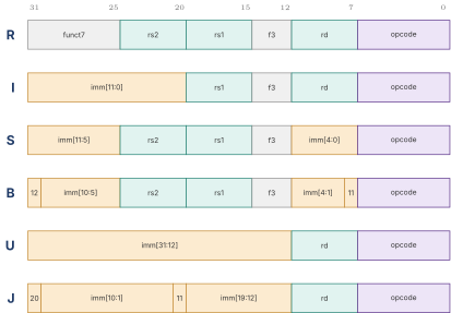
Read down the columns rather than across the rows and the design becomes visible. The rs1 column at bits 19:15 is teal in R, I, S, and B. The rs2 column at 24:20 is teal in R, S, and B. The rd column at 11:7 is teal in R, I, U, and J and amber in S and B, meaning the immediate stole exactly the field that was not needed. And bit 31 is amber in every single format that has an immediate at all.
2.4 Why the immediate is scrambled, from first principles
This is a classic interview question and it has a precise answer that most candidates get half right. The half most people give is "the sign bit is always at bit 31." That is true and it is one of three constraints. Here are all three, and then the arithmetic that shows what they are worth.
Constraint one: the sign bit is always instruction bit 31. Every RISC-V immediate is sign-extended to XLEN bits. Sign extension means replicating the top bit of the immediate across all the bits above it. In a 64-bit machine an I-type's twelve-bit immediate must be replicated into bits 63 down to 12, which is 52 copies of one wire. If the sign bit lived at a different instruction bit depending on the format, you would need a mux in front of that 52-way fanout, and that mux would sit at the head of the longest fanout in the decoder. By pinning the sign bit to instruction bit 31 in every format, the fanout driver's input is a single wire with no logic in front of it, so sign extension proceeds in parallel with the opcode decode instead of after it.
Constraint two: an immediate bit should come from as few different instruction bits as possible. The decoder ultimately produces one 64-bit immediate value regardless of format. Think of that as a function from instruction bits to immediate bits. In the worst imaginable design, any immediate bit could come from any instruction bit, and you would need a 32-to-1 multiplexer for each of 32 immediate output bits. RISC-V instead arranged that most immediate bits have only one possible source, and none has more than four.
Constraint three: never shift. Branch and jump offsets are in units of two bytes, so encoding them requires multiplying by two, which in hardware is a shift by one. A shift by a constant is free if you do it by wiring, and expensive if you do it with logic. RISC-V does it by wiring. The B and J formats place their immediate bits so that lands in the instruction bit that an I-type would use for , and so on. The spec's own rationale states that rotating the bits in the B and J encodings, rather than using dynamic multiplexers to multiply the immediate by two, reduces instruction signal fanout and immediate multiplexer cost by roughly a factor of two.
Now the table that makes all three visible at once. For each output immediate bit, this is where it comes from in each format.
| Immediate bit | I-type | S-type | B-type | U-type | J-type | Distinct sources |
|---|---|---|---|---|---|---|
| inst[31] | inst[31] | inst[31] | inst[31] | inst[31] | 1 | |
| inst[31] | inst[31] | inst[31] | inst[30:20] | inst[31] | 2 | |
| inst[31] | inst[31] | inst[31] | inst[19:12] | inst[19:12] | 2 | |
| inst[31] | inst[31] | inst[7] | inst[20] | 4 | ||
| inst[30:25] | inst[30:25] | inst[30:25] | inst[30:25] | 2 | ||
| inst[24:21] | inst[11:8] | inst[11:8] | inst[24:21] | 3 | ||
| inst[20] | inst[7] | 3 |
Count the rows carefully, because the shape of the distribution is the answer. One row, , has a single source and needs no mux at all. Five rows need only a 2-to-1 or a 3-to-1. And one single bit, , needs a 4-to-1. Everything above bit 31 is sign extension driven from that same one wire.
Count the two-input muxes that implies. A 3-to-1 costs two 2-to-1s and a 4-to-1 costs three.
Thirty-eight two-input multiplexers. Compare against the naive alternative where any of 32 immediate bits could come from any of 32 instruction bits, which is two-input muxes. That is a factor of roughly 26 in area, and, more importantly, the depth falls from five levels of mux to at most two. At 3 GHz, five levels of 2-to-1 mux at perhaps 25 ps each is 125 ps of a 333 ps cycle spent on nothing but shuffling immediate bits. Two levels is 50 ps. Those gate counts are illustrative rather than taken from a real library, but the ratio is the point and the ratio is robust.
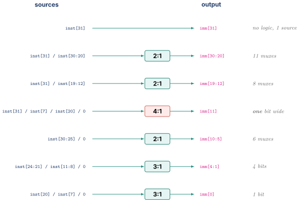
One honest caveat to add unprompted when you give this answer. The saving is real but it is a saving in the simplest implementations. A wide out-of-order machine that decodes six instructions per cycle has six immediate generators, so the area saving multiplies, but that machine also has separate dedicated adders for branch targets and load addresses and would not have been limited by an immediate mux anyway. The design was optimized for the cheap end of the range and costs the expensive end essentially nothing. Saying that shows you understand who the optimization was for.
The cost the design pays is entirely on the software side. A human reading a hex instruction dump has to reassemble a branch offset from four scattered pieces, and an assembler, a disassembler, and a linker relocation all have to implement the scramble. That is a one-time software cost paid by a handful of tool authors against a per-chip hardware saving paid by every implementer, which is the trade the committee made deliberately.
2.5 No condition codes, and what that costs
Here is how Arm A64 branches on a comparison.
| cmp x1, x2 // subtract, discard the result, set the NZCV flags | |
| b.lt target // branch if the N and V flags say "less than" |
cmp is not a separate opcode. It assembles to subs xzr, x1, x2, a subtract whose result is thrown into the zero register purely so the flags get written. Note that the destination is xzr and not x0. Unlike RISC-V, A64's x0 is an ordinary argument register, and the zero register lives only in the 32nd specifier slot as described above.
Two instructions, then, and a hidden piece of architectural state in between: NZCV, four condition flags for negative, zero, carry, and overflow. x86-64 has the same idea in EFLAGS with more flags.
Here is how RISC-V does it.
| blt x1, x2, target // compare and branch, one instruction |
RISC-V has no condition codes at all. There is no flags register. Branches read two registers, compare them internally, and branch. The six branch instructions are beq, bne, blt, bge, bltu, and bgeu, the last two being the unsigned comparisons.
Why, from a hardware point of view. A flags register is a piece of architectural state that a very large fraction of instructions write. That creates three problems, each of which is real in a high-performance implementation.
It is a serialization point unless you rename it. In an out-of-order machine, per Out of Order Execution, every write to a shared architectural resource creates a write-after-write dependency. If every arithmetic instruction wrote NZCV and NZCV were not renamed, the machine could have only one flag-setting instruction in flight. So high-performance Arm and x86 implementations rename the flags exactly like a register. That is extra rename ports, extra physical storage, and extra recovery machinery on a misprediction, all of which RISC-V simply does not build.
Partial writes are worse than full writes. On x86, inc updates some flags and leaves the carry flag alone. A subsequent instruction that reads the whole flags word therefore depends on two producers, the last instruction to write the non-carry flags and the last instruction to write carry, and the hardware must merge them. That partial-flag merge is a genuine and well-documented source of stalls in x86 implementations. RISC-V has no flags and therefore no merge.
It costs an instruction slot and a code-size increase in the common case. Arm's compare-then-branch is two instructions where RISC-V's is one. Arm compensates with CBZ and CBNZ for the compare-against-zero cases, which are the most common.
Now the honest cost side, because an interviewer will push here and "there is no downside" is the wrong answer.
The branch itself is longer. blt x1, x2, target must perform a 64-bit magnitude comparison and then decide taken or not-taken, all inside the branch resolution path. Arm's b.lt reads a pre-computed bit. The RISC-V spec's own rationale acknowledges this and argues that the comparison fits in a regular pipeline stage, but on a very deep, very high-frequency machine the comparator is real work sitting in the branch resolve loop, and it is a place where an aggressive implementation may need to pre-compute the condition earlier.
You cannot compare once and branch several times. A loop that tests the same condition at several points recomputes the comparison each time.
Branchless code lost its natural instruction. Arm has CSEL and x86 has CMOV, which select between two values without a branch. That matters enormously for unpredictable branches, per Front End and Branch Prediction, and for constant-time cryptographic code, per Security Side Channels and Speculation, where a data-dependent branch is a side channel. RISC-V originally had nothing. The Zicond extension eventually added czero.eqz and czero.nez, which conditionally zero a register and from which a select can be built in two instructions, and Zicond is mandatory in RVA23. The ISA had to add the capability back. Volunteering that is a strong move in an interview because it shows you can criticize the design you are being hired to implement.
2.6 PC-relative addressing with only two instructions
A 32-bit instruction cannot hold a 64-bit address, or even a 32-bit one. Every architecture needs a way to build a large constant or reach a distant address, and RISC-V's answer is unusually spare.
LUI rd, imm20, load upper immediate, places a 20-bit immediate into bits 31:12 of rd, zeroing the low 12 bits, then sign-extends bit 31 into the upper 32 bits on RV64. AUIPC rd, imm20, add upper immediate to PC, does the same but adds the result to the address of the AUIPC instruction itself.
Those two, paired with a 12-bit immediate on the instruction that follows, cover everything.
To build the constant 0x12345678, note that the low twelve bits, 0x678, are positive as a signed twelve-bit number, so no correction is needed:
| lui x5, 0x12345 // x5 = 0x12345000 | |
| addi x5, x5, 0x678 // x5 = 0x12345678 |
There is a subtlety worth knowing because it comes up in assembler questions. The addi immediate is signed, so if the low twelve bits have their top bit set, the addi subtracts and you must pre-compensate by adding one to the upper immediate. Assemblers do this automatically for the li pseudo-instruction, and forgetting it is the classic first bug when hand-writing RISC-V.
To reach a symbol anywhere within GiB of the current instruction:
| auipc x5, %pcrel_hi(sym) | |
| addi x5, x5, %pcrel_lo(sym) |
That GiB reach comes straight from the arithmetic: 20 bits of upper immediate shifted left by 12 gives a 32-bit signed range, which is bytes. It is the reason position-independent code on RISC-V is cheap. There is no global-offset-table indirection needed for local symbols and no literal pool sitting in the instruction stream the way Arm A32 needed one.
2.7 What RV64I changes, and the sign-extension rule
RV64I widens the registers to 64 bits and adds a set of instructions ending in W: ADDW, SUBW, SLLW, SRLW, SRAW, ADDIW, SLLIW, SRLIW, SRAIW. These operate on the low 32 bits and produce a 32-bit result.
The rule that governs them is worth memorizing because it is a favorite question. A W instruction sign-extends its 32-bit result into all 64 bits of the destination register. Not zero-extends. Sign-extends.
Concrete. If x6 holds 0x0000_0000_8000_0000 and you execute addiw x5, x6, 0, the 32-bit result is 0x8000_0000, whose top bit is 1, so x5 receives 0xFFFF_FFFF_8000_0000.
Why sign-extend? Because it means a 32-bit signed integer has exactly one canonical 64-bit representation, and therefore the 64-bit comparison instructions work correctly on 32-bit values with no conversion. blt on two sign-extended 32-bit values gives the right answer. If the convention were zero-extension, you would need separate 32-bit comparison instructions. Arm A64 took the other path, providing W-register forms of essentially everything with zero-extension into the X register, which is a larger encoding cost for a different convenience.
Here is the interview trap hiding in all of this. LWU exists and LW zero-extends nothing. LW loads a 32-bit value and sign-extends it. LWU loads a 32-bit value and zero-extends it. Likewise LB/LBU and LH/LHU. The sign-extending form is the default because signed integers are the common case in C.
03.Part 3, the extension mechanism
3.1 The standard extensions, and what each one costs to build
The base is I. Everything below is separately optional, and for each one the interesting question is not what it does but what it forces you to build.
M, integer multiply and divide. MUL, MULH, MULHU, MULHSU, DIV, DIVU, REM, REMU, plus W variants on RV64. MULH returns the upper XLEN bits of the full XLEN product, which is how you get a 128-bit result on a 64-bit machine in two instructions. Building it means a multiplier array and a divider, both from Arithmetic Hardware, and the divider is the expensive, iterative, rarely-used block that Part 5 of Power Fundamentals and Clock Gating uses as its canonical operand-isolation example. One detail with teeth: RISC-V integer division does not trap on divide by zero. Dividing by zero returns all ones for DIV and the dividend for REM. On signed overflow, meaning the most negative number divided by , DIV returns the dividend and REM returns zero, which is the arithmetically correct remainder and is worth getting right because the two cases have different answers. Software checks if it cares. That removes a whole exception class from the pipeline, which is a genuine simplification in an out-of-order machine where a late-arriving exception is expensive.
A, atomics. Two families. The AMOs are AMOSWAP, AMOADD, AMOAND, AMOOR, AMOXOR, AMOMIN, AMOMAX, and the unsigned min/max, each of which atomically reads a memory location, applies an operation, writes back, and returns the old value. The load-reserved / store-conditional pair, LR and SC, is the general mechanism: LR reads a location and establishes a reservation, SC writes it only if the reservation is still intact and returns zero on success. As of recent spec versions the two families are separable as Zalrsc and Zaamo, because a cacheless microcontroller can implement AMOs but cannot reasonably implement reservations.
F and D, single and double precision floating point. These add a separate 32-entry floating-point register file, f0 through f31, plus the fcsr control and status register holding the rounding mode and the accrued exception flags. That separate register file is the significant architectural cost: it is more state to save on a context switch, more rename resources in an out-of-order machine, and it needs its own load and store instructions. Note that F and D follow IEEE 754 and RISC-V, unlike x87, does not do arithmetic at an extended internal precision. Zfh adds half precision.
C, compressed instructions. 16-bit encodings for the most common operations. Gets its own subsection below because of what it does to the fetch unit.
V, vectors. Part 6.
B, bit manipulation. Ratified in 2024 as the union of three sub-extensions. Zba is address generation: sh1add, sh2add, sh3add compute rs2 + (rs1 << n) in one instruction, which collapses the shift-and-add that array indexing generates constantly, plus add.uw for unsigned-word indices. Zbb is basic bit manipulation: count leading and trailing zeros, population count, byte reverse, min/max, andn/orn/xnor, sign extension, and rotates. Zbs is single-bit set, clear, invert, and extract. Zbc, carry-less multiply, is separate and is optional in RVA23. It is the primitive for GCM and CRC, which is why it turns up in cryptography discussions.
Zicsr, control and status register access, and Zifencei, instruction-fetch fence. These were carved out of the base I set in 2019, and the carve-out is instructive. A tiny embedded core with no CSRs at all should not be required to implement CSRRW. Zifencei, meanwhile, provides FENCE.I, which makes previously executed stores visible to instruction fetch, needed by any self-modifying code or JIT.
3.2 The C extension, and what it costs the fetch unit
C provides 16-bit encodings for common instructions with common operands: a c.addi with a small immediate, a c.lw with a small offset off a common base register, a c.mv, a c.j. Roughly a quarter to a third of static code size is commonly quoted as the saving on general-purpose code, and the mechanism is straightforward. The most frequent instructions use a small number of registers and small immediates, so a restricted 16-bit encoding covers most dynamic instructions.
How a decoder tells 16-bit from 32-bit is elegant. If instruction bits 1:0 are anything other than 11, it is a 16-bit instruction. If they are 11 and bits 4:2 are not 111, it is a 32-bit instruction. Longer encodings extend the same pattern. So the length is determined by the two lowest bits, which is one 2-input decode away from the raw fetch data.
Now the cost, and this is the part that separates people who have built a front end from people who have read about one.
Instructions become 2-byte aligned, so a 32-bit instruction can straddle anything. With C enabled, a 32-bit instruction may begin at any even address. That means it can straddle a cache line boundary, in which case the fetch unit needs two cache accesses to assemble one instruction. Worse, it can straddle a page boundary, in which case the second half may take a page fault while the first half did not, and the machine must handle a fault reported partway into an instruction it has not finished fetching. Both cases must be built, both are rare, and both are exactly where fetch-unit bugs live. Front End and Branch Prediction covers the alignment machinery this forces.
Decode width becomes variable. A 4-wide decoder fed 16 bytes might see four 32-bit instructions, or eight 16-bit ones, or any mixture. The decoders must be preceded by length-decode and alignment logic that figures out where each instruction starts before the real decode can begin. That is a genuine serial dependency in the front end, and it is the same problem x86 has in a far worse form.
Branch target alignment gets murkier. With C, JAL and branches can target any even address, so the fetch unit cannot assume 4-byte alignment anywhere.
The honest summary to give is that C is close to free in code size and instruction-cache pressure, and it is not free in front-end complexity. An embedded core wants it unambiguously. A very wide superscalar core pays a real price and takes it anyway because instruction-cache footprint matters more.
3.3 The naming scheme, so a string is readable
Single letters are reserved for the historical extensions. Everything newer is a multi-letter name, and the first letter after the prefix tells you the category.
| Prefix | Meaning | Examples |
|---|---|---|
Z | unprivileged standard extension | Zicsr, Zifencei, Zba, Zbb, Zbs, Zicond, Zfh, Zk* for crypto, Zv* for vector sub-extensions |
S | supervisor-level extension | Sv39, Sv48, Svnapot, Svpbmt, Sstc, Ssaia |
H | hypervisor | the H extension itself |
X | non-standard, vendor-specific | anything a vendor invents |
Within Z, the second letter groups by area: Zi is base-adjacent infrastructure, Zb is bit manipulation, Zf and Zd are floating point, Za is atomics, Zk is scalar cryptography, Zv is vector. So Zvbb reads as "vector bit-manipulation" and Zknh as "scalar crypto, NIST hashing" without looking anything up.
Here is the practical point for an interview. When someone says "we implement RV64GCV_Zba_Zbb_Zbs_Zicond," you should be able to read that as "general purpose, compressed, vectors, the mandatory bit-manipulation set, and conditional zero," and immediately think "that is approximately an RVA23 target."
3.4 The encoding space, and the four custom opcodes
Return to bits 6:0 of a 32-bit instruction. Seven bits gives 128 major opcodes, but the low two bits must be 11 for a 32-bit instruction, so the real space is bits 6:2, which is 32 major opcodes. Most are allocated to standard use: OP, OP-IMM, OP-32, OP-IMM-32, LOAD, STORE, BRANCH, JAL, JALR, LUI, AUIPC, MISC-MEM, SYSTEM, the floating-point opcodes, and so on.
Four are reserved for you. They are named custom-0 through custom-3, and the spec states that future standard extensions will avoid them.
| Name | inst[6:0] | Hex | Note |
|---|---|---|---|
custom-0 | 0001011 | 0x0B | |
custom-1 | 0101011 | 0x2B | |
custom-2 | 1011011 | 0x5B | also marked for future RV128 |
custom-3 | 1111011 | 0x7B | also marked for future RV128 |
The last two carry a caveat. They are marked as reserved for a future 128-bit RISC-V, so a design expecting a very long life might prefer the first two.
Beyond whole major opcodes there is a second, finer resource. Within an existing major opcode such as OP, the funct7 and funct3 fields are not fully allocated, so unused combinations are available. The community vocabulary for these two approaches is worth knowing.
A greenfield extension takes one of the custom-* major opcodes and defines whatever encoding it likes inside it. You get the full 25 remaining bits to structure however you want, and you are guaranteed not to collide with a standard extension. The cost is that you burn one of only four such opcodes.
A brownfield extension reuses an existing major opcode and an unused funct combination inside it. It is far cheaper in encoding space, it can reuse the existing instruction format so the decoder and immediate generator need no changes at all, and it risks colliding with a future standard extension that claims the same combination.
For an interview, the useful judgment is: brownfield when the instruction fits an existing format exactly and you accept the collision risk, greenfield when you need a genuinely different operand structure or when you are building a product with a long lifetime and cannot take the risk.
3.5 Adding a custom instruction, the full checklist
Several of these roles screen on custom instructions and hardware/software co-design, so this deserves to be a rehearsed answer rather than an improvised one. The mistake almost everyone makes is to answer only the first item.
One, pick the encoding. Greenfield or brownfield per 3.4. Decide the format: does it need two sources and one destination, an immediate, a wider result? If it fits an existing format, say R, the decoder change is a handful of new funct7/funct3 decodes and nothing else.
Two, work out what it does to the pipeline. How many cycles? Is it pipelined or iterative? If iterative, it needs a stall or a scoreboard interlock, which touches hazard logic per CPU Foundations Pipeline and Hazards. Does it need a new bypass path, per Part 4 of Execution Units? In an out-of-order machine, does it fit an existing issue port or does it need its own, per Part 3 of Execution Units?
Three, decide what exceptions it can raise, and whether it is precise. This is where custom instructions go wrong. If the instruction touches memory it can page fault, and the fault must be precise, meaning the machine can be restarted at that instruction with all architectural state as it was before. If the instruction is long-running and updates state incrementally, you either make it restartable from the beginning, which wastes work, or you add architectural state recording partial progress, which is exactly what the vector extension's vstart register does and it is not a small addition.
Four, count the architectural state you are adding. This is the item that kills more proposals than any other. If the instruction reads or writes any state that is not an existing x register, that state is now part of the context and the operating system must save and restore it on every context switch, and on every signal delivery, and ptrace and the debugger and the core-dump format must know about it. That is a kernel patch, a libc patch, and an ABI change. An instruction that operates purely on existing general-purpose registers costs the software stack almost nothing. An instruction with a private accumulator costs it a great deal.
Five, get it through the toolchain. Take the levels in ascending order of effort. Hand-encoding with the assembler's .insn directive works today with no toolchain change. Adding assembler mnemonic support comes next. Then compiler intrinsics, so C code can call it. Then teaching the compiler's instruction selector to generate it automatically, which is the hardest and often is never done. Be realistic about which level you are proposing, because "the compiler will just use it" is usually false.
Six, arrange discovery. How does software know the instruction exists? The misa CSR reports only the single-letter extensions and is coarse. For anything else the practical answers are the device tree or ACPI tables at boot, and on Linux a hwprobe-style system call for user space. A binary that unconditionally executes your custom instruction will take an illegal-instruction trap on every other implementation.
Seven, verify and debug it. It needs to appear in the disassembler or every trace and core dump is unreadable. It needs a reference model, per Verification Methodology, and if it has any interesting arithmetic that reference model is real work. If it is at all subtle, formal is the right tool.
The strong version of this answer names all seven and says which are cheap and which are not. The cheap ones are encoding and toolchain assembly support. The expensive ones are precise exceptions, added architectural state, and OS enablement, and the last two are the reason most proposed custom instructions never ship.
3.6 Deciding whether to add one at all
Before any of that, there is an arithmetic question, and answering it first is the difference between an engineer and an enthusiast.
Suppose profiling shows a cryptographic inner loop takes 30 percent of total runtime, and a custom instruction would make that loop four times faster. Amdahl's law:
A 29 percent speedup for a new instruction, a decoder change, a toolchain change, a verification effort, and a kernel patch. That is probably not worth it.
Change one number. Suppose the loop is 70 percent of runtime and the instruction gives ten times:
A 2.7 end-to-end speedup is worth a great deal of engineering.
The asymptote is the other half of the argument. Even an infinitely fast custom instruction on the 30-percent kernel caps out at . Knowing the ceiling before you start is the whole point, and quoting it unprompted is a strong signal. It also connects directly to Performance Modeling, which is where the profile that produces the 30 percent comes from in the first place.
04.Part 4, RVWMO, the memory model, in its own terms
4.1 Two harts, four instructions, one outcome that should not happen
A hart, hardware thread, is RISC-V's word for an independent instruction stream. One physical core with two-way multithreading has two harts.
Two harts share memory. Locations data and flag both start at 0.
| Hart 0 Hart 1 | |
| li t0, 42 spin: lw t2, 0(a1) # read flag | |
| sw t0, 0(a0) # data = 42 beqz t2, spin # wait for flag | |
| li t1, 1 lw t3, 0(a0) # read data | |
| sw t1, 0(a1) # flag = 1 |
Hart 0 writes the data, then raises a flag. Hart 1 waits for the flag, then reads the data. This is the message-passing pattern and it is how essentially every producer-consumer queue, every lock release, and every "the DMA finished" handshake is written.
The question: can hart 1 observe flag == 1 and then read data == 0?
Every intuition says no. Hart 0 wrote data before flag. Hart 1 read flag before data. If hart 1 saw the second write, surely it must see the first.
Under RVWMO, yes, it can happen, and for two independent reasons. As written, this code is broken.
Reason one, on hart 0. Nothing in RVWMO orders two stores to different addresses. Hart 0 may make flag = 1 visible to other harts before data = 42. Physically this happens in a store buffer that retires entries out of order, or in a non-blocking cache where the flag line was already in the modified state and the data line had to be fetched.
Reason two, on hart 1. Nothing in RVWMO orders two loads to different addresses either, and, crucially, the branch between them does not help. A control dependency from a load to a later load is not preserved. Hart 1's machine can speculate past the branch and issue the lw of data before the lw of flag has even returned. If it does, it reads data from a moment before hart 0 wrote it, and the value 0 is sitting in a register long before the branch resolves.
The fix requires a fence on each side.
| Hart 0 Hart 1 | |
| sw t0, 0(a0) # data = 42 spin: lw t2, 0(a1) # read flag | |
| fence w, w beqz t2, spin | |
| sw t1, 0(a1) # flag = 1 fence r, r | |
| lw t3, 0(a0) # read data |
fence w,w on hart 0 says: every store before me becomes visible before any store after me. fence r,r on hart 1 says: every load before me is performed before any load after me. With both, the outcome is forbidden. With only one, it is not.
That worked example is the whole memory model in miniature. Everything below is machinery for saying it precisely.
4.2 Global memory order, and the shape of the definition
RVWMO's definition has an unusual shape and understanding the shape is most of the battle.
Start with memory operations. A load or store instruction generates one or more memory operations. RVWMO reasons about the operations, not the instructions, which matters because a misaligned access or a vector access may generate several.
RVWMO then posits a global memory order: a single total order over all memory operations from all harts in a given execution. Every store appears somewhere in this order, every load appears somewhere, and a load reads the value written by the latest store to the same address that precedes it in the global order, or the latest store from its own hart that precedes it in program order, whichever is later.
The trick is that the global memory order is not required to agree with program order. It is required to agree with program order only where preserved program order says it must.
So the entire content of RVWMO is the definition of preserved program order. Everything else is bookkeeping. A concurrent program is correct if and only if every global memory order consistent with preserved program order yields acceptable results.
Two properties of that framing are worth naming because they distinguish RVWMO from some other relaxed models. Memory operations are ordered with respect to a single global order, so RVWMO is a multi-copy-atomic model. There is no execution in which two different harts disagree about the order in which two stores became visible. Use the precise term if you are pushed on it, because both the RISC-V and the Arm specifications do. The property is other-multi-copy atomicity. A store becomes visible to every other hart at the same instant, but the hart that issued it may see it earlier than anyone else, because it can forward the value out of its own store buffer. Arm A64's model became other-multi-copy atomic as of Armv8, and Power's is not multi-copy atomic at all, which is why Power reasoning is harder. And the model is defined in terms of syntactic dependencies rather than semantic ones, which is 4.4 and is the single subtlest thing in the whole specification.
4.3 The thirteen rules of preserved program order
Two operations and from the same hart, with before in program order and both accessing regular main memory, are in preserved program order if any of thirteen rules applies. They group into four families.
Overlapping addresses, rules 1 through 3. Rule 1: is a store and and access overlapping addresses. Rule 2: and are both loads, some byte is read by both, no store to that byte lies between them in program order, and the two loads return values written by different memory operations. Rule 3: is generated by an AMO or a successful SC, is a load, and returns the value written by .
Rule 2 deserves a sentence in plain language because it is easy to misread. It does not say two loads of the same address are always ordered. It says that if they return values written by different stores, they must be ordered, which is exactly the constraint that forbids reading backwards in time. A younger load of a location may not return an older value than an older load of the same location returned. In hardware that is the coherence-of-read-read check that a load queue performs, per Load Store and Memory Ordering.
Explicit synchronization, rules 4 through 8. Rule 4: a FENCE instruction orders before . Rule 5: carries an acquire annotation. Rule 6: carries a release annotation. Rule 7: and both carry RCsc annotations. Rule 8: and are a paired LR and SC.
Syntactic dependencies, rules 9 through 11. Rule 9: has a syntactic address dependency on . Rule 10: has a syntactic data dependency on . Rule 11: is a store and has a syntactic control dependency on .
Rule 11 is the one that explains the message-passing failure in 4.1. The control dependency rule covers only the case where is a store. A control dependency ending in a load is not preserved. That is deliberate. Forbidding speculation past a branch to a load would forbid the single most important optimization a modern front end performs. Arm A64 makes exactly the same choice for exactly the same reason.
Pipeline dependencies, rules 12 and 13. Rule 12: is a load, some store between and in program order has an address or data dependency on , and returns the value written by . Rule 13: is a store and some instruction between and in program order has an address dependency on .
These two exist because real machines forward from a store buffer, and forwarding creates an ordering that the earlier rules do not capture. They are the least intuitive rules and the least likely to be asked about. Knowing they exist and that they exist because of store-to-load forwarding is enough.
Here is the single most useful summary to have memorized. Under RVWMO, none of load-load, load-store, store-store, or store-load to different addresses is ordered by default. Ordering comes only from fences, from acquire/release annotations, or from a syntactic dependency.
4.4 Syntactic dependencies, and why the word "syntactic" carries the weight
A syntactic address dependency of instruction on instruction means that uses some register to compute its address, and 's value is produced through a chain of register writes reaching back to . A syntactic data dependency is the same with being the source of the data being stored. A syntactic control dependency means some branch or indirect jump between and depends on .
The word syntactic is doing an enormous amount of work, and here is why. Consider:
| lw a0, 0(s0) # i | |
| xor a1, a0, a0 # a1 is always 0 | |
| add a2, s1, a1 # a2 == s1, always | |
| lw a3, 0(a2) # j |
The value in a2 does not actually depend on the value loaded into a0, because a0 XOR a0 is zero regardless. Semantically there is no dependency at all. Syntactically there is, because there is an unbroken chain of register writes from a0 to a1 to a2, and a2 is j's address register.
RVWMO says is ordered after . The dependency counts even though the value does not.
Why define it this way? Because the alternative is unusable. A semantic definition would require the memory model to specify exactly which value-flow optimizations a compiler or a processor is allowed to see through, and there is no clean place to draw that line. A syntactic definition is mechanically checkable. A tool can look at the register dataflow graph and decide, and so can a person.
The hardware consequence is the interesting part, and it is worth saying out loud in an interview. A machine that optimizes away a false dependency must not thereby break the ordering. If your rename stage recognizes xor a1, a0, a0 and breaks the dependency by producing a zero immediately, you have removed the ordering RVWMO promised. In practice implementations either do not perform that optimization on the address path, or they enforce the load-load ordering by another mechanism such as a load-queue check. Value prediction is the sharper version of the same problem. Predicting a loaded value and using it to compute an address before the load returns removes the dependency entirely. I would want to check the current spec's exact discussion before asserting a definitive answer here. What I am confident of is that the tension is real, the spec acknowledges it, and it is a legitimate thing to raise as a question rather than to answer glibly.
The historical contrast is the best way to remember why RISC-V preserves address dependencies at all. Alpha did not. On Alpha, a load whose address came from a previous load could execute before that load, which broke pointer chasing so badly that Linux grew a dedicated barrier for it. Every subsequent architecture, Arm and RISC-V included, preserves address dependencies to loads, and that is why the read-copy-update discipline in the kernel works without an explicit barrier on the read side.
4.5 The FENCE instruction, bit by bit
FENCE is encoded in the MISC-MEM major opcode and is the only base instruction whose whole meaning lives in a bitmask.
| Field | Instruction bits | Meaning |
|---|---|---|
fm | 31:28 | fence mode, 0000 for a normal fence |
PI | 27 | predecessor set includes device input |
PO | 26 | predecessor set includes device output |
PR | 25 | predecessor set includes memory reads |
PW | 24 | predecessor set includes memory writes |
SI | 23 | successor set includes device input |
SO | 22 | successor set includes device output |
SR | 21 | successor set includes memory reads |
SW | 20 | successor set includes memory writes |
The semantics are one sentence: every operation in the predecessor set that precedes the fence in program order is ordered before every operation in the successor set that follows the fence in program order.
So fence rw, rw sets PR, PW, SR, SW and is the full barrier. fence w, w sets PW and SW and orders only store-to-store. fence r, r orders only load-to-load. fence rw, w is the release-style fence you place before a flag store. fence r, rw is the acquire-style fence you place after a flag load.
Four bits on each side gives sixteen possible sets per side, so 256 combinations, of which a handful are useful. The finer granularity is the point. On Arm A64 you get DMB SY, DMB LD, and DMB ST and their inner-shareable variants, which is a coarser menu. Whether the extra granularity buys real performance depends entirely on the implementation, and an honest answer says so. A simple machine may implement every fence as a full drain and lose nothing. An aggressive machine can implement fence w,w as a store-buffer ordering constraint that does not stall loads at all, which is a genuine win.
The I and O bits are the separate device-ordering axis, and they exist because RISC-V distinguishes ordering of accesses to regular main memory from ordering of accesses to I/O regions, where a read can have a side effect. fence io, io is the device fence. Conflating the two is a common error. A driver that uses fence rw, rw where it needed fence iorw, iorw can be subtly wrong.
FENCE.TSO is a special encoding, fm = 1000 with predecessor and successor both rw. It orders load-to-load, load-to-store, and store-to-store, but leaves store-to-load unordered. That is precisely the x86-TSO ordering, and it exists so that code translated from x86 does not need a full barrier where TSO gave it three-quarters of one for free.
Finally, FENCE.I is a different instruction in a different extension, Zifencei. It orders instruction fetch with respect to data writes on the same hart, and you need it after writing code you intend to execute. It says nothing about other harts, which is why making a JIT work across harts requires an IPI to every hart that might have stale instruction-fetch state.
4.6 Acquire, release, and the atomics
The AMO instructions and LR/SC carry two bits in their encoding, aq and rl.
Setting aq gives the operation an acquire annotation, meaning no memory operation after it in program order may be reordered before it. Setting rl gives it a release annotation, meaning no memory operation before it may be reordered after it. Setting both makes it a full barrier for that hart.
The vocabulary to have straight is RCpc versus RCsc, and the difference is invisible until you look at one specific pair of instructions, so look at that pair first. Put a releasing operation and then an acquiring operation back to back on the same hart, which is exactly what a thread does when it drops one lock and immediately takes another.
| amoswap.w.rl x0, x0, (a0) # release lock A | |
| amoswap.w.aq t1, t0, (a1) # acquire lock B |
Read what each annotation promises on its own. The rl says "nothing before me sinks below me." The aq says "nothing after me floats above me." Neither one says anything whatsoever about the other instruction, because the release's constraint looks backwards and the acquire's looks forwards, and there is no rule stitching them together. So under RCpc, release consistency with processor-consistent synchronization, those two operations are not ordered against each other, and another hart may observe lock B being taken before lock A was dropped.
Under RCsc, release consistency with sequentially consistent synchronization, they are ordered, and all the annotated operations across all harts appear in one total order.
RISC-V's aq and rl on AMOs and LR/SC are RCsc, and preserved program order rule 7 is the rule that says so. Two RCsc-annotated operations are ordered against each other, which is precisely the stitch the pair above was missing. That is a stronger and simpler guarantee than the RCpc alternative and it is the reason an amoswap.w.aqrl works as a general lock acquire. Arm made the same choice for LDAR and STLR, and then added an explicitly RCpc load, LDAPR, in Armv8.3 for code that does not need the stronger form and would rather not pay for it.
A lock, written out, makes the annotations concrete.
| acquire: | |
| li t0, 1 | |
| 1: amoswap.w.aq t1, t0, (a0) # swap 1 into the lock, acquire | |
| bnez t1, 1b # if the old value was 1, someone holds it | |
| ret | |
| release: | |
| amoswap.w.rl x0, x0, (a0) # store 0, release | |
| ret |
The aq on acquire prevents anything inside the critical section from floating up above the lock acquisition. The rl on release prevents anything inside from sinking below the lock release. Remove either annotation and the critical section leaks.
Plain loads and stores cannot carry aq or rl in the base model. That was a real gap. A C11 atomic_load_explicit(..., memory_order_acquire) on a plain word had to be compiled as a load followed by fence r, rw, which is heavier than Arm's single LDAR, and a store-release had to become fence rw, w followed by a store.
The gap has since been closed, and this is a place where a stale answer will cost you. Zalasr, the atomic load-acquire and store-release extension, is ratified. It adds lb.aq, lh.aq, lw.aq, and ld.aq on the load side and sb.rl, sh.rl, sw.rl, and sd.rl on the store side, with aqrl forms of each, and the annotations are RCsc exactly like the ones on the AMOs. LLVM and QEMU support it and the Linux kernel has picked it up. It is not in RVA23, which was ratified before it, so a binary that has to run on any RVA23 machine still emits the fence sequence. The useful thing to say is therefore the whole arc: the base model has no load-acquire, the fence sequence is the portable fallback, and the ISA has since grown the single-instruction form as a separate ratified extension that profiles have not yet absorbed.
LR/SC and forward progress. LR establishes a reservation on a reservation set containing the addressed word. The set may be larger than the word, and how much larger is implementation-defined, which is why two threads doing LR/SC on adjacent words can livelock each other on some implementations. SC succeeds only if the reservation is still valid, returning 0, and fails returning nonzero.
The spec places a real obligation on the implementation. A constrained LR/SC loop, meaning at most 16 instructions laid out sequentially in memory, containing between the LR and SC only base-I instructions and excluding loads, stores, backward jumps, taken backward branches, JALR, FENCE, and SYSTEM instructions, is guaranteed to eventually make progress. Concretely, the execution environment must guarantee that eventually either this hart's SC succeeds, or some other hart performs a store or AMO to the reservation set, or some device writes it. Meeting that guarantee is a hardware design obligation with teeth. It means your reservation mechanism must not be able to be starved indefinitely by another hart's traffic, and it constrains how aggressively a cache can steal a line away from a hart that has just taken a reservation. The 16-instruction limit exists so the hardware can bound how long a reservation must be held.
4.7 Where RVWMO sits, against x86-TSO and Arm A64
Now the comparison, and the discipline is to have described RVWMO first in its own terms, which Parts 4.1 through 4.6 did, so that the table is a summary rather than a definition.
| Reordering of, different addresses | Sequential consistency | x86-TSO | Arm A64 | RVWMO |
|---|---|---|---|---|
| load then load | no | no | yes | yes |
| load then store | no | no | yes | yes |
| store then store | no | no | yes | yes |
| store then load | no | yes | yes | yes |
| address dependency to a load preserved | n/a | n/a | yes | yes |
| data dependency to a store preserved | n/a | n/a | yes | yes |
| control dependency to a load preserved | n/a | n/a | no | no |
| control dependency to a store preserved | n/a | n/a | yes | yes |
| other-multi-copy atomic | yes | yes | yes (Armv8) | yes |
The table's shape is the headline. RVWMO and Arm A64 agree on every row. That is not a coincidence. RVWMO was designed to be close enough to Arm's model that concurrent software written and reasoned about for Arm, including the Linux kernel's entire memory-model discipline, transfers without rethinking. The differences are in the instructions provided rather than in the ordering permitted. Arm had LDAR and STLR as single instructions from the start where RISC-V's base model needed fences around plain accesses, a gap Zalasr has since closed but no profile yet requires, and RISC-V has a much finer fence bitmask where Arm has a small menu of DMB variants.
The Linux kernel's barrier mappings are worth memorizing because they make the model tangible: smp_mb() is fence rw, rw, smp_rmb() is fence r, r, smp_wmb() is fence w, w.
Against x86-TSO the difference is one row that matters enormously in practice. Under TSO, store-then-load is the only reordering permitted, which is why so much x86 concurrent code is accidentally correct and why so much of it breaks when ported. Under RVWMO everything is reorderable. A candidate who has only ever debugged concurrency on x86 will underestimate this. Saying so is a good way to show you understand the porting hazard.
4.8 What a weak model buys the hardware
The last question, and the one that ties the model back to the reader's own discipline. Why not just build TSO and make everyone's life easier?
Store buffer drain. Under TSO, stores must become visible in program order. That constrains the store buffer to retire in order, so one store missing in the cache blocks every store behind it. Under RVWMO, a store buffer may retire out of order, so a store that hits can pass a store that missed. The cost of a store miss stops being a serialization point.
Load speculation without recovery. Under TSO a load may not be reordered with a later load, so a machine that issues loads out of order must detect when a coherence invalidation exposes the reordering and roll back. That is real hardware: a load queue entry per in-flight load, a snoop comparison against every entry, and a pipeline flush when it hits. Under RVWMO the reordering is architecturally legal, so the machinery needed for that particular case shrinks. It does not disappear, because rule 2 still requires the same-address coherence check, but the general different-address case does not need it.
Coherence and interconnect ordering. Cache Coherence Protocols and Interconnect and AMBA describe how much of an interconnect's complexity is about maintaining ordering guarantees end to end. A weaker model lets the interconnect complete transactions in whatever order is efficient over a much wider range of cases.
The counter-argument, which you should give in the same breath, is that x86 has shipped extremely high-performance TSO machines for decades, so a weak model is clearly not necessary for performance. What it does is make the same performance cheaper in area and verification effort, and it moves a burden onto software that software has largely learned to carry through language-level memory models such as C11 and the kernel's own discipline. That is the honest framing, and it is more convincing than "weak is faster."
05.Part 5, the privileged specification
5.1 Three modes, and which combinations are legal
RISC-V defines three privilege modes.
Machine mode, M, is the highest privilege and the only mandatory one. It has unrestricted access to everything. Firmware runs here.
Supervisor mode, S, is where an operating system kernel runs. It gets its own set of control registers and, crucially, control of address translation.
User mode, U, is where applications run.
Only three combinations are legal, and each corresponds to a real class of machine.
| Modes | Class of machine | Protection mechanism |
|---|---|---|
| M only | deeply embedded microcontroller | none |
| M, U | embedded with process isolation | PMP, physical memory protection |
| M, S, U | Unix-class | MMU, plus PMP for the M/S boundary |
The middle row deserves a paragraph because it is a genuinely RISC-V-flavored answer. Physical Memory Protection is a set of M-mode CSRs, pmpcfg0 and up plus pmpaddr0 and up, that define up to 64 physical address regions with read, write, and execute permissions and a lock bit. It is a range-based protection scheme with no translation and no page tables, and it gives you isolation on a machine with no MMU at all. It also protects M-mode firmware from a supervisor. A locked PMP entry cannot be changed even by M-mode until reset. That combination, isolation without translation, is exactly what a real-time controller wants, and it has no clean equivalent in the Arm A-profile world, though Arm's R-profile MPU is the same idea.
The H extension adds hypervisor support by splitting supervisor mode. HS is the hypervisor-extended supervisor mode where a hypervisor runs. VS and VU are virtualized supervisor and user, where a guest OS and its applications run. Two-stage address translation follows. The guest's page tables map guest virtual to guest physical, and a second set of tables under the hypervisor's control maps guest physical to real physical. Arm's equivalent is EL2 with stage-1 and stage-2 translation, and the structure is genuinely similar.
Against Arm A64's four exception levels, the mapping is close but not exact. EL0 is U, EL1 is S, EL2 is HS, and EL3 is a secure monitor with no direct RISC-V equivalent in the base privileged spec. RISC-V's M mode sits below everything as firmware rather than as a separate security world, and the security-world role is filled by a separate extension family.
5.2 CSRs, and the trick hidden in their addresses
Control and status registers are the privileged architecture's state. They are addressed in a 12-bit space, so up to 4096 of them, and they are read and written by six instructions from the Zicsr extension.
CSRRW rd, csr, rs1 atomically reads the CSR into rd and writes rs1 into it. CSRRS reads and then sets every bit that is 1 in rs1. CSRRC reads and clears. The three immediate forms, CSRRWI, CSRRSI, CSRRCI, take a 5-bit unsigned immediate instead of a register.
Two encoding rules make the set complete without extra opcodes. If rd is x0, CSRRW must not read the CSR at all, which matters because reading some CSRs has side effects. If rs1 is x0, CSRRS and CSRRC must not write the CSR at all. So csrr rd, csr, a pure read, is CSRRS rd, csr, x0, and csrw csr, rs1, a pure write, is CSRRW x0, csr, rs1. Both are pseudo-instructions over the same encodings.
Now the trick, and it is one a logic designer will appreciate immediately. Decode three CSR numbers by hand before reading any rule, the same way Part 1 decoded an instruction word.
mstatus is CSR number 0x300, which in binary is 0011 0000 0000. sstatus is 0x100, which is 0001 0000 0000. And cycle, the free-running cycle counter that user code is allowed to read but nobody is allowed to write, is 0xC00, which is 1100 0000 0000.
Pull bits 11:10 out of each: 00, 00, and 11. Pull bits 9:8 out of each: 11, 01, and 00. Now line those up against what you already know about the three registers. The first two are writable and the third is not, and 11 in bits 11:10 belongs to exactly the one that is not. The first is reachable only from M-mode, the second from S-mode down, the third from U-mode up, and bits 9:8 hold , , and , which are the privilege-mode numbers for M, S, and U.
Nothing about those three numbers was arbitrary. The 12-bit CSR address encodes its own access policy.
Bits 11:10 encode whether the register is read-write or read-only. The value 11 means read-only. Bits 9:8 encode the lowest privilege mode that may access it. So the entire permission check is a comparison of two bit-fields taken straight out of the instruction against the current privilege mode, with no lookup table and no per-CSR permission ROM. An access that violates either rule raises an illegal-instruction exception.
That is a decode-stage simplification of the same character as the fixed register fields in 2.2. Put the information the control logic needs into fixed bit positions so the control logic is a comparator instead of a table. The naming convention follows: mstatus and friends begin with m and live in M-accessible addresses, sstatus and friends begin with s.
One structural detail catches people. Several S-mode CSRs are restricted views of the M-mode ones. sstatus is a subset of mstatus reading the same underlying bits, and sie and sip are the supervisor-visible subsets of mie and mip. They are not separate storage. An interviewer asking "what happens if S-mode writes sstatus" is testing whether you know it modifies the same physical bits mstatus sees.
5.3 A trap, step by step
A trap is any transfer of control into a more privileged mode. RISC-V divides them into exceptions, which are synchronous and caused by the current instruction, and interrupts, which are asynchronous.
Take a concrete one. A user program executes lw a0, 0(a1) and the page containing that address is not mapped. Suppose no delegation is configured, so the trap goes to M-mode. Here is exactly what the hardware does, in order.
One. mepc receives the virtual address of the faulting lw. Not the next instruction, the faulting one, because a page fault is restartable and after the OS maps the page the instruction must run again. For an ECALL the OS must add 4 itself, which is a classic first-kernel bug.
Two. mcause receives the cause. The top bit, bit MXLEN, is 0 for an exception and 1 for an interrupt. The remaining bits hold the code. A load page fault is 13. Store or AMO page fault is 15, instruction page fault is 12, illegal instruction is 2, breakpoint is 3, and environment calls from U, S, and M modes are 8, 9, and 11.
Three. mtval receives the faulting virtual address. For an illegal-instruction exception it may instead receive the offending instruction bits, which saves the handler a fetch.
Four. mstatus updates its privilege stack. MPIE, bit 7, receives the old value of MIE, bit 3. Then MIE is cleared to 0, disabling interrupts. Then MPP, bits 12:11, receives the privilege mode we came from, which here is U.
Five. The privilege mode becomes M and the program counter becomes mtvec.
mtvec has a MODE field in its low two bits. MODE = 0 is Direct. All traps go to BASE. MODE = 1 is Vectored. Asynchronous interrupts go to , while exceptions still go to BASE. Four bytes per vector slot is exactly one instruction, so each slot must be a jump. Vectored mode removes the cause decode from the interrupt path, which matters for interrupt latency in a real-time system.
MRET reverses all of it. MIE receives MPIE, the privilege mode becomes whatever MPP held, MPIE is set to 1, MPP is set to the least-privileged supported mode, and the program counter becomes mepc.
The reason MPP is reset to the least-privileged mode on return is a security hardening. It makes it harder for a later bug to accidentally return to a higher privilege than intended. That is the kind of detail that reads as "has actually read the spec" when volunteered.
5.4 Delegation, and the cost it removes
There is a problem with what 5.3 just described. On a Unix-class machine, a page fault taken in user mode is the kernel's business, and the kernel runs in S-mode. But every trap goes to M-mode by default, so every page fault would enter M-mode firmware, which would then have to manufacture a synthetic trap into S-mode. Every syscall, every page fault, every timer tick would cost two trap entries and two returns.
Delegation removes that. Two M-mode CSRs, medeleg for exceptions and mideleg for interrupts, are bitmaps indexed by cause code. Setting bit 13 of medeleg means that a load page fault, when it occurs in S-mode or U-mode, is delivered directly to S-mode.
When a trap is delegated, everything in 5.3 happens against the S-mode registers instead. sepc, scause, stval, and stvec take the roles of their M-mode counterparts, and sstatus's SPP, SPIE, and SIE bits take the role of MPP, MPIE, and MIE. SPP is a single bit rather than two, because S-mode can only have come from S or U. SRET returns.
Two rules constrain delegation and both are worth stating. A trap is never delegated to a mode less privileged than the one in which it occurred. A page fault taken while already in S-mode is not delegated to U-mode. It stays in S. And traps taken in M-mode are never delegated at all, because there is nowhere higher to come from.
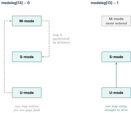
There is a real cost to naming here. Without delegation, a syscall-heavy workload pays two full trap entries per syscall, and a trap entry on a deep out-of-order machine is a pipeline flush plus a privilege change, which is easily on the order of a hundred cycles. Doubling that on every syscall is not a marginal effect. Delegation is not an optimization, it is the thing that makes M-mode firmware viable at all.
5.5 Sv39, worked with a real address
Now the concrete part. Take a specific virtual address and walk it all the way to a physical address, arithmetic included.
The address. .
Sv39's shape. A 39-bit virtual address, split into three 9-bit page-table indices and a 12-bit page offset. Bits 63 down to 39 must all equal bit 38, exactly like a sign extension. An address that violates that rule faults immediately, which is what makes the address space a valid low half and a valid high half with a huge hole in between. Here bit 38 is 0 and the upper bits are 0, so the address is legal.
Where do the numbers come from? A 4 KiB page needs 12 bits of offset. A page table is itself one 4 KiB page, and each entry is 8 bytes, so a table holds entries, needing index bits. Three levels gives bits. That is the entire derivation, and it also tells you Sv48 is the same thing with four levels and Sv57 with five.
Decompose the address. Write the low 39 bits of 0x8004_2AB8 in binary and slice it. Thirty-nine, not thirty-two, because VPN[2] runs from bit 38 up past the top of the low word. Bits 38 down to 32 are all zero here, which is why the hex looks like a 32-bit number.
So VPN[2] is 2, VPN[1] is 0, VPN[0] is 66, and the offset is 0xAB8, which is 2744 decimal. Small enough to keep in your head, which was the point of choosing this address.
The satp register. satp is 64 bits: MODE in bits 63:60, ASID in bits 59:44, and PPN in bits 43:0. MODE = 8 selects Sv39, 9 selects Sv48, 10 selects Sv57, and 0 means Bare, no translation at all. The ASID field is up to 16 bits and tags TLB entries so a context switch need not flush.
Say the root page table lives at physical address 0x8020_0000. Its physical page number is . With ASID 0:
The page table entry format. Each PTE is 8 bytes.
| Bits | Field | Meaning |
|---|---|---|
| 0 | V | valid |
| 1 | R | readable |
| 2 | W | writable |
| 3 | X | executable |
| 4 | U | accessible from U-mode |
| 5 | G | global, present in every address space |
| 6 | A | accessed |
| 7 | D | dirty |
| 9:8 | RSW | reserved for supervisor software |
| 18:10 | PPN[0] | |
| 27:19 | PPN[1] | |
| 53:28 | PPN[2] | |
| 60:54 | reserved | |
| 62:61 | PBMT | page-based memory type, with Svpbmt |
| 63 | N | NAPOT contiguity hint, with Svnapot |
The three PPN pieces are contiguous, occupying bits 53:10 as a single 44-bit physical page number, giving a 56-bit physical address space. And here is the rule that makes the walk work: if R, W, and X are all zero and V is one, the entry is a pointer to the next-level table. Otherwise it is a leaf. The combination R = 0, W = 1 is reserved and faults, because writable-but-not-readable is meaningless.
The walk, three memory accesses.
Level 2. The walker computes the PTE address as the root table's physical base plus the index times 8.
It reads eight bytes from there. Say the value is 0x2008_0401. Decode: bit 0 is 1, so valid. Bits 3:1 are 0, so R = W = X = 0, so this is a pointer. The PPN is bits 53:10, which is . So the next-level table is at .
Level 1.
Say it reads 0x2008_0801. Valid, RWX = 0, so another pointer, PPN , next table at 0x8020_2000.
Level 0.
Say it reads 0x22AC_04D7. The low byte is 0xD7 , so V = 1, R = 1, W = 1, X = 0, U = 1, G = 0, A = 1, D = 1. Readable, writable, not executable, user-accessible, already accessed and dirty. Since R is set this is a leaf. The PPN is .
The answer.
Note that the page offset passed through untouched, which is true in every paging scheme and is the reason the TLB lookup can proceed in parallel with an L1 cache access on a virtually-indexed cache, per Part 6 of Virtual Memory and Memory Ordering.
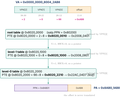
What this costs. Three dependent memory accesses on a TLB miss, each of which may itself miss in the data cache. That is why every implementation caches intermediate PTEs in page-walk caches, and why huge pages matter, which is Part 4 of Virtual Memory and Memory Ordering.
5.6 Superpages, the A and D bits, and SFENCE.VMA
Superpages come for free from the pointer-versus-leaf rule. If the level-1 entry has R, W, or X set, the walk stops there and the entry is a leaf mapping a 2 MiB page, because VPN[0] and the 12-bit offset together become a 21-bit offset. Stopping at level 2 gives a 1 GiB page. Sv39's three sizes are therefore 4 KiB, 2 MiB, and 1 GiB.
There is a constraint with a memorable failure mode. A superpage's physical address must be aligned to the superpage size, which means the unused low PPN fields must be zero. A 2 MiB leaf requires PPN[0] == 0. A 1 GiB leaf requires PPN[1] == PPN[0] == 0. If they are not, the hardware raises a misaligned superpage page fault rather than silently doing something reasonable. That is a real class of kernel bug and a fair interview question.
Unlike Arm, RISC-V has only a 4 KiB base page size. Arm A64 offers 4 KiB, 16 KiB, and 64 KiB granules. RISC-V's answer to the same problem is Svnapot, which sets bit 63 of a PTE to say "this entry and a naturally-aligned power-of-two run of neighbouring entries all map contiguous physical memory," letting a TLB store one entry instead of sixteen. It is a hint to the TLB rather than a different table geometry, which is arguably the cleaner mechanism and is certainly the cheaper one to add later.
The A and D bits. A records that the page has been accessed, D that it has been written. Historically the spec allowed two behaviors: either the hardware sets them during the walk, or the hardware raises a page fault when it finds them clear and lets software set them. That choice is unusual, and it meant portable kernel code had to handle both. The Svadu extension standardizes hardware updating. Hardware A/D update is not free. Setting a bit in a PTE is an atomic read-modify-write to memory performed by the page-table walker, which means the walker needs write capability and coherent access, which is a real design cost.
SFENCE.VMA rs1, rs2 is the TLB maintenance instruction. It orders page-table writes made by this hart before it against implicit page-table reads made after it. rs1 optionally names a virtual address and rs2 optionally names an ASID. x0 in either position means "all." So sfence.vma x0, x0 is the full flush, sfence.vma a0, x0 invalidates one address across all ASIDs, and sfence.vma x0, a1 invalidates one ASID entirely.
The critical property to state is what it does not do. SFENCE.VMA is local to the hart that executes it. There is no broadcast. Invalidating a mapping on a multi-hart system requires the software to send an inter-processor interrupt to every other hart and have each execute its own SFENCE.VMA, which is the notorious TLB shootdown. Arm A64 took the other path. TLBI instructions broadcast to the inner-shareable domain in hardware. That is one of the sharpest architectural differences between the two, it has a large software cost on RISC-V, and it is a fine thing to raise when asked to compare them.
5.7 Against Arm A64, the differences that matter
| RISC-V | Arm A64 | |
|---|---|---|
| privilege modes | M, S, U, plus HS/VS/VU with H | EL0 to EL3 |
| translation control | one satp per hart | TTBR0_EL1 and TTBR1_EL1, split by address |
| base page sizes | 4 KiB only, plus Svnapot hints | 4 KiB, 16 KiB, 64 KiB granules |
| levels at 39 bits | 3 | 3 at the 4 KiB granule |
| TLB invalidation | SFENCE.VMA, hart-local | TLBI, broadcasts |
| address space ID | ASID in satp | ASID in TTBR |
| trap vector | mtvec/stvec, direct or vectored | VBAR_ELn with a fixed 16-entry layout |
| isolation without an MMU | PMP | MPU in the R-profile |
The TTBR0/TTBR1 row deserves a sentence because its consequences reach further than it looks. Arm gives each address space two table base registers, one used for low addresses and one for high, so a kernel can install its own mapping in TTBR1 once and never replicate it. RISC-V has one satp, so the kernel's mapping must be present in every process's page table, which means kernel PTEs are duplicated across every address space and marked global. That has both a memory cost and a security consequence. Be careful with the security half, because the sloppy version of it is wrong. Meltdown was caused by a speculative load being allowed to use data it had no permission to read before the permission check retired. Having the kernel mapped into every user address space is not what created the vulnerability, it is what made the vulnerability worth exploiting, because it put the entire kernel within reach of a user-mode address. RISC-V's single satp reproduces that always-mapped structure, x86-64's single CR3 has it too, and Arm's split TTBR0/TTBR1 is the design that does not. The knock-on cost is on the mitigation side. Page-table isolation means swapping the root pointer on every kernel entry and exit, which is more disruptive when there is only one root pointer to swap. Security Side Channels and Speculation carries that argument.
06.Part 6, the vector extension
6.1 One loop, three machines, the same binary
Start concrete, and start with the problem rather than the solution.
You want to add two arrays of 32-bit floats, elementwise, with elements. Here is how you write it in RISC-V vector assembly. Registers on entry: a0 holds , a1, a2, a3 point at the two sources and the destination.
| loop: | |
| vsetvli t0, a0, e32, m1, ta, ma # t0 = how many elements this pass | |
| vle32.v v8, (a1) # load t0 elements from x | |
| vle32.v v16, (a2) # load t0 elements from y | |
| vfadd.vv v24, v8, v16 # add them | |
| vse32.v v24, (a3) # store t0 elements to z | |
| slli t1, t0, 2 # t0 elements * 4 bytes each | |
| add a1, a1, t1 | |
| add a2, a2, t1 | |
| add a3, a3, t1 | |
| sub a0, a0, t0 # elements remaining | |
| bnez a0, loop |
Read the first instruction as a question and an answer. vsetvli t0, a0, e32, m1, ta, ma says: "I have a0 elements left and I want to work on 32-bit elements. How many can you do?" The hardware writes its answer into t0 and into an internal register called vl, and every vector instruction that follows operates on exactly vl elements.
Now run that identical binary on three machines with different vector register widths, with .
| Machine | VLEN | Elements per pass | Full passes | Final pass | Total passes |
|---|---|---|---|---|---|
| A | 128 bits | 4 | 250 | 3 | 251 |
| B | 256 bits | 8 | 125 | 3 | 126 |
| C | 512 bits | 16 | 62 | 11 | 63 |
Three different machines. One binary. No recompilation, and no separate cleanup loop for the leftover elements, because the final pass is the same four instructions with a smaller vl.
Compare against how you write the same thing with x86 AVX, whose vector register is 256 bits wide and is named at that width in the instruction encoding. (The intrinsics below are AVX. AVX2 widened the integer operations to 256 bits, and people routinely say "AVX2" for the whole 256-bit generation, but the float add itself is AVX.)
    int i = 0;
    for (; i + 8 <= n; i += 8)                       // 8 floats, hard-coded
        _mm256_storeu_ps(z + i, _mm256_add_ps(_mm256_loadu_ps(x + i),
                                              _mm256_loadu_ps(y + i)));
    for (; i < n; i++)                               // scalar epilogue
        z[i] = x[i] + y[i];
The 8 is baked into the source. Running this on an AVX-512 machine gets you half the available width unless you recompile with different intrinsics. And the epilogue loop is not optional. With it runs three scalar iterations, and for small the epilogue can be most of the work.
That contrast is the whole case for vector-length agnostic programming, and it is worth being able to state in thirty seconds.
6.2 The four quantities, and the register that holds three of them
Four numbers determine what a vector instruction does. Keep them straight and everything else follows.
VLEN is the width in bits of one architectural vector register, v0 through v31. It is a property of the hardware, fixed at design time, and it does not appear anywhere in any instruction encoding. It must be a power of two and the spec caps it at bits. Software can read VLEN/8 from the read-only vlenb CSR.
ELEN is the widest element the implementation supports, at least 8 and a power of two. Also fixed hardware.
SEW, selected element width, is the size of each element right now, in bits: 8, 16, 32, or 64. Software sets it.
LMUL, the length multiplier, is how many vector registers are glued together into one logical register right now: 1, 2, 4, 8, or the fractions , , . Software sets it.
From those, the derived quantity everything depends on:
That is the largest number of elements a single instruction can process. Read it as: LMULVLEN bits of register space, divided into SEW-bit elements.
Work the table for VLEN = 256, because seeing the numbers move is worth more than the formula.
| SEW | LMUL | LMUL | LMUL | LMUL | LMUL |
|---|---|---|---|---|---|
| 8 | 16 | 32 | 64 | 128 | 256 |
| 16 | 8 | 16 | 32 | 64 | 128 |
| 32 | 4 | 8 | 16 | 32 | 64 |
| 64 | 2 | 4 | 8 | 16 | 32 |
SEW and LMUL, plus two policy bits, live in a CSR called vtype.
vtype bits | Field | Meaning |
|---|---|---|
| 2:0 | vlmul | LMUL, as a signed exponent: 000 1, 001 2, 010 4, 011 8, 101, 110, 111 |
| 5:3 | vsew | SEW: 000 8, 001 16, 010 32, 011 64 |
| 6 | vta | tail agnostic |
| 7 | vma | mask agnostic |
| XLEN | vill | this vtype is illegal |
The vlmul encoding is worth a glance because it explains the fractions. It is read as a signed three-bit exponent and LMUL . So 111 is and gives , 110 is and gives , 101 is and gives . 100 would be and is reserved. The fractions are not a bolted-on special case. They are the natural continuation of the encoding.
The fifth quantity, vl, the number of elements that will actually be processed, is its own CSR and is set by vsetvl.
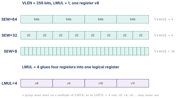
6.3 vsetvli, exactly
There are three forms. vsetvli rd, rs1, vtypei takes the requested element count from register rs1 and the new vtype from an immediate. vsetivli rd, uimm, vtypei takes both from immediates, useful for a fixed small count. vsetvl rd, rs1, rs2 takes both from registers, which is what you need when the vtype is computed at run time.
The requested count is called AVL, application vector length. The rules for turning AVL into vl are more subtle than "take the minimum," and the subtlety is a good interview question.
- If , then .
- If , then .
- If , then
vlmay be anything satisfying , at the implementation's discretion.
The middle case, where AVL sits strictly between VLMAX and twice VLMAX, looks like sloppiness and is the opposite. Suppose VLMAX is 8 and 9 elements remain. Under a strict minimum rule you would get vl = 8 then vl = 1, and the second pass wastes seven eighths of the machine. That freedom lets the implementation return vl = 5, then vl = 4, so both passes are nearly full. On a long-latency vector unit that is a real win, and it costs software nothing because the loop is written to handle whatever vl it is given.
Two special encodings complete the picture. rs1 = x0 with rd not x0 means "set vl to VLMAX," used when you want maximum width regardless of a count. rs1 = x0 and rd = x0 means "keep the current vl, change only vtype," which is what you want when switching element width mid-loop. Be exact about the guard rail on that one, because the spec is careful and a loose paraphrase is catchable. This form may only be used when the new SEW/LMUL ratio leaves VLMAX unchanged. Using it with a ratio that would change VLMAX is reserved, and implementations are permitted to set vill in that case but are not required to. Saying flatly "it sets vill" describes one implementation's choice, not the architecture's promise, and reserved-versus-required is exactly the distinction an ISA interviewer is listening for.
vill. If a vsetvl requests a configuration the implementation genuinely does not support, say SEW = 64 on a machine with ELEN = 32, the hardware does not trap. It sets vtype.vill, zeroes the rest of vtype, and zeroes vl. Any subsequent vector instruction that depends on vtype then raises an illegal-instruction exception. The indirection exists so that software can probe for support by executing a vsetvl and reading back vtype, without needing an exception handler to do feature detection.
6.4 LMUL, and why the fractions exist
LMUL greater than 1 is easy to motivate. It processes more elements per instruction. At VLEN = 256, SEW = 32, LMUL = 8 gives VLMAX = 64, so one vfadd.vv does 64 additions. The cost is register pressure. Grouping eight physical registers into one logical register leaves logical registers, and a group must start at a register number that is a multiple of LMUL, so at LMUL = 8 only v0, v8, v16, v24 may name a group. A kernel needing six live vectors cannot use LMUL = 8 without spilling.
So LMUL is a software-controlled trade between elements-per-instruction and architectural register count, made at run time by writing a CSR. Nothing in AVX or NEON has an analogue. It is genuinely the most unusual idea in the extension.
The fractions are less obvious and the motivation is worth working through, because it is a favorite follow-up.
Consider a widening operation: read 16-bit elements, produce 32-bit results. vwadd.vv does exactly this. The problem is that the destination elements are twice as wide, so if the source group is LMUL = 1 the destination needs LMUL = 2, and the two operands' element counts must match for the operation to make sense.
Now put it in a loop that processes 16-bit inputs into 32-bit outputs. You set SEW = 16 for the sources. You want the destination at SEW = 32. With VLEN = 256, SEW = 16, LMUL = 1 gives VLMAX = 16. The destination at SEW = 32 needs LMUL = 2 to hold 16 elements, which is fine. But you have now consumed three registers' worth of space for a two-register operation, and the arithmetic gets awkward when you chain several widening steps.
Fractional LMUL fixes this by letting the source occupy less than a whole register. Set SEW = 16 with LMUL and you get VLMAX elements occupying half a register. Widen to SEW = 32 at LMUL = 1 and you get 8 elements occupying one whole register. The element counts match, and no register group is larger than one register. That is what the fractions are for. They keep VLMAX constant across a change in element width, so mixed-width code does not have to renumber its registers.
The rule to remember and quote: VLMAX depends only on the ratio LMUL/SEW. Halve SEW and halve LMUL and VLMAX is unchanged. That ratio is sometimes called SEW/LMUL and it is the invariant mixed-precision code holds fixed.
6.5 Tail and mask policies, vstart, and the mask register
Masking. Any vector instruction can be predicated. The vm bit in the encoding, when 0, means "use v0 as the mask," and element is active only if bit of v0 is 1. The mask always comes from v0. There is no choice of mask register. That is a deliberate simplification versus SVE's sixteen predicate registers, and it costs software an occasional mask move.
Tail elements. Elements from vl up to VLMAX are the tail. They are not being computed this pass, so what happens to them in the destination register?
Inactive elements. Elements below vl whose mask bit is 0 are inactive. Same question.
vta and vma answer them. Set to 0 the policy is undisturbed. The destination register's existing contents at those positions are preserved. Set to 1 the policy is agnostic. The hardware may leave them alone or may overwrite them with all ones, at its discretion.
Why offer the agnostic option at all? Because undisturbed is expensive. Preserving the old contents means the destination register is a source operand of every masked instruction, which creates a read-after-write dependency on the previous value and forces the hardware to read a register it otherwise would not. Agnostic frees the implementation to write the whole register unconditionally. On a renaming machine it is the difference between needing a merge and not. Compilers emit ta, ma by default for exactly this reason, which is why the loop in 6.1 has it.
vstart. A vector instruction at LMUL = 8 with SEW = 8 on a wide machine may touch thousands of elements. If a load faults on element 900, restarting from element 0 wastes the work and, worse, may be wrong if the destination overlaps a source. vstart is a CSR recording the element index at which the next vector instruction should begin. A trap can set it, and the instruction resumes from there. Software normally does not touch it, but hardware has to implement it, and it is a genuine design cost. Your vector load/store unit must be able to report how far it got, and your vector instructions must be able to start in the middle.
6.6 Why this is not AVX with different names
Four differences, in descending order of how fundamental they are.
One, the register width is not in the instruction encoding. vfadd.vv v24, v8, v16 contains no width. The machine's VLEN supplies it at run time. In AVX, vaddps ymm0, ymm1, ymm2 names a 256-bit register in the encoding. Going to 512 bits required a new register file, zmm, a new prefix, EVEX, new mask registers k0 through k7, and hundreds of new opcodes. Every widening in the x86 SIMD lineage, from SSE to AVX to AVX2 to AVX-512, was an ISA extension with a full opcode set. RVV widens by building wider hardware and changing nothing in the ISA.
Two, vl eliminates the epilogue. The tail elements are handled by the same instructions with a smaller vl. Fixed-width SIMD needs a scalar cleanup loop or a masked final iteration written specially. That is not just source-code convenience. The epilogue is extra code in the instruction cache and extra branches for the predictor, and for short arrays it can dominate.
Three, LMUL is a run-time knob with no analogue. Software can decide, per loop, whether to trade register count for work per instruction.
Four, the front-end amortization is explicit and large. This is the point that matters most to a hardware designer and it is the one to lead with in an interview. VLEN is not the same as the datapath width. An implementation may have VLEN = 512 with a 128-bit execution datapath and simply take four cycles per vector instruction, processing one 128-bit chunk at a time. From the ISA's point of view nothing changed. From the front end's point of view, one fetch, one decode, one issue, one register-file access set, and one retire now cover four times as much arithmetic.
That is the classical Cray-style temporal vector machine, and it is why RVV is attractive for area-constrained designs in a way that fixed-width SIMD is not. Fetch, decode, rename, and issue are a large fraction of a modern core's power, per Part 2 of Power Fundamentals and Clock Gating, and amortizing them over four times the work is a direct energy-per-operation win. A machine that wants more throughput later widens the datapath to 256 or 512 bits and runs the same code faster with the same instruction count.
The honest counterpoint, which you should offer before being asked, is that the same decoupling means performance is not portable even though the binary is. Two RVA23-conformant machines with the same VLEN can differ by a factor of four in vector throughput because one has a wider datapath. Software that wants to tune has to measure, and library authors have found that harder than the "write once, run fast everywhere" story suggests.
6.7 Against Arm SVE
Arm's Scalable Vector Extension is the other production vector-length-agnostic design, so the comparison is the sharpest available.
| RISC-V V | Arm SVE / SVE2 | |
|---|---|---|
| vector-length agnostic | yes | yes |
| register width | VLEN, a power of two, up to bits | 128 to 2048 bits, in 128-bit steps |
| element count control | a vl CSR set by vsetvl | no vl, a predicate register per loop |
| loop idiom | vsetvli then work then sub and branch | whilelt generating a predicate, then work, then incb and branch |
| predication | one mask register, v0 | 16 predicate registers, p0 to p15 |
| register grouping | LMUL, run-time, to 8 | none |
| element width | SEW in vtype, run-time | encoded in the instruction |
| tail handling | smaller vl on the last pass | predicate false for the tail lanes |
The structural difference underneath the table is where the "how many elements" state lives. RVV puts it in an architectural CSR that one instruction sets and every subsequent instruction reads. SVE puts it in a predicate register produced by a compare-like instruction and consumed explicitly by each instruction that wants it.
Each choice has a cost. RVV's vtype and vl are implicit state that every vector instruction depends on, which means a renaming machine must track them and a vsetvl is effectively a barrier for vector instructions that follow. SVE's predicates are explicit operands, which costs encoding bits on every instruction but keeps the dependency visible to the renamer. SVE also encodes element width in the opcode, so it needs more opcodes than RVV but avoids the mode-switch dependency.
I would not claim SVE expertise in an interview beyond this level. The table above and the "where does the length live" framing is defensible. Anything deeper about SVE2 or SME I would flag as something I have read about rather than used.
6.8 What the hardware actually has to build
Because this is the part a design interview will push on, here is what implementing RVV commits you to beyond the arithmetic.
A second large register file. Thirty-two registers at VLEN bits each. At VLEN = 512 that is 2 KiB of state, versus 256 bytes for the integer registers. That is more state to save on a context switch, more area, and, if the machine renames, a physical vector register file substantially larger again.
Renaming at group granularity, if you rename. An instruction at LMUL = 8 reads and writes eight architectural registers. A renamer that allocates one physical register per architectural register must allocate eight, and a machine that renames the group as a unit must handle the case where LMUL changes mid-stream. This is one of the harder parts of putting RVV into an out-of-order core, and it is fair to say so.
vtype and vl as implicit dependencies. Every vector instruction reads them. Getting that wrong is easy and the failure is subtle.
Restartability via vstart. As in 6.5.
A load/store unit that handles unit-stride, strided, indexed, and segmented accesses. RVV's memory instructions include constant-stride loads, gather/scatter with a vector of indices, and segment loads that de-interleave structures of two to eight fields on the fly. The segment forms are wonderful for software and are a substantial load/store unit design problem, per Load Store and Memory Ordering.
A decision about chaining. A classical vector machine forwards elements from one instruction to the next as they are produced rather than waiting for the whole vector, which is chaining. Whether to build it, and how it interacts with the bypass network of Execution Units, is a real microarchitectural choice.
07.Part 7, interrupts, the CLINT, the PLIC, and debug
7.1 Three kinds of interrupt, and where each comes from
RISC-V defines exactly three interrupt sources per privilege level, and knowing why there are three rather than a hundred is the key to the whole area.
Software interrupts are one hart poking another. This is the inter-processor interrupt, used for TLB shootdowns and scheduler wakeups.
Timer interrupts come from a monotonic time counter reaching a per-hart compare value.
External interrupts are everything else in the system: a UART, a network controller, a storage device.
The mip and mie CSRs, machine interrupt pending and machine interrupt enable, hold one bit per source per level, at fixed positions.
| Bit | Name | Meaning |
|---|---|---|
| 1 | SSIP | supervisor software |
| 3 | MSIP | machine software |
| 5 | STIP | supervisor timer |
| 7 | MTIP | machine timer |
| 9 | SEIP | supervisor external |
| 11 | MEIP | machine external |
Three sources, two levels, six bits. The design decision is that the ISA does not specify how interrupts are generated, only how they are delivered. Everything about prioritizing dozens of device interrupts, masking them, and routing them to particular harts happens in a memory-mapped device outside the core, and the core sees only a single "external interrupt pending" bit. That is why the CLINT and the PLIC are separate specifications rather than part of the ISA.
7.2 The CLINT, and one bug it causes
The Core-Local Interruptor handles the software and timer interrupts. It originated as a SiFive design that became a de facto standard through adoption, and it has since been reworked into the ACLINT specification, which splits the same functionality into separate MSWI, MTIMER, and SSWI devices at separate base addresses while remaining layout-compatible with the old CLINT. I would hedge on the exact ratification status of ACLINT in an interview rather than assert it.
It exposes three kinds of memory-mapped register.
msip, one 32-bit register per hart. Writing 1 to bit 0 sets that hart's mip.MSIP. Writing 0 clears it. That is the entire IPI mechanism, a store from one hart into another hart's msip word.
mtime, a single 64-bit free-running counter shared by all harts, incrementing at a fixed frequency.
mtimecmp, one 64-bit register per hart. Hardware continuously compares and sets mip.MTIP for that hart whenever .
The conventional layout, which comes from the SiFive design and is what QEMU's virt machine implements, places the CLINT at base 0x0200_0000 with msip at offset 0, mtimecmp at 0x4000, and mtime at 0xBFF8. Those addresses are convention, not architecture, and a platform is free to put them elsewhere. Software finds them from the device tree.
Work an example. Suppose mtime ticks at 10 MHz, which is the common QEMU convention. To schedule an interrupt in 1 millisecond:
Now the bug that this design causes, which is worth naming because it catches essentially everyone writing their first RISC-V kernel. mip.MTIP is read-only and is not cleared by acknowledging the interrupt. It is a purely level-driven comparison. The only way to make it go away is to write a new, larger mtimecmp. A handler that services the timer and returns without touching mtimecmp re-enters immediately and forever. Clearing mie.MTIE masks it but does not clear it.
There is a second, subtler issue. On RV32 mtimecmp is 64 bits accessed as two 32-bit stores, and writing the low half first can transiently create a compare value in the past, firing a spurious interrupt. The standard fix is to write 0xFFFF_FFFF to the high half first, then the low half, then the real high half.
Sstc is the extension that adds stimecmp, a supervisor-level compare register. Without it, an S-mode kernel cannot program a timer directly and must call M-mode firmware through the SBI to do it, which is a trap and a return on every timer reprogram. With it, the kernel writes its own CSR. That is a real and easily-explained performance improvement and a good example of the privileged spec evolving in response to measured cost.
7.3 The PLIC, and the claim/complete handshake
The Platform-Level Interrupt Controller handles external interrupts. Its job is to take some number of wired interrupt lines from devices and decide which one, if any, a given hart at a given privilege level should be told about.
Four concepts.
Sources are numbered from 1 upward. Source 0 is reserved and means "no interrupt." That reservation is what makes the claim register self-describing. A read returning 0 means nothing was pending.
Priority is a per-source value. Priority 0 means "never interrupt," which is how a source is effectively disabled globally.
Contexts are the things that receive interrupts, and a context is a (hart, privilege level) pair. A four-hart machine supporting M and S mode has eight contexts. Each context has its own enable bitmap, one bit per source, and its own priority threshold. Only sources with priority strictly greater than the threshold are delivered.
Claim and complete is a single memory-mapped register per context that behaves differently on read and write.
Reading the claim register atomically does three things: it returns the ID of the highest-priority pending source that is enabled for this context, it clears that source's pending bit, and it marks the source as being serviced by this context. Writing that same ID back to the register signals completion, which allows the source to interrupt again.
Why an explicit two-step rather than an automatic acknowledge? Because the gap between claim and complete is exactly the window in which the device's own interrupt condition is cleared. If the PLIC re-armed the source at claim time, a level-triggered device that has not yet been serviced would immediately re-assert and the handler would spin. The completion write says "I have talked to the device and it has stopped asking."
Work a small example. Three sources: source 3 at priority 5, source 7 at priority 2, source 9 at priority 5. Hart 0's S-mode context has all three enabled and a threshold of 1. Sources 7 and 9 both go pending.
Source 9's priority, 5, beats source 7's, 2, so a read of the claim register returns 9. Both exceed the threshold of 1, so both are eligible. Source 7 stays pending and sip.SEIP remains set, so after completing 9 the handler will loop and claim 7. If the threshold had been 4, source 7 would never be delivered to this context at all.
If sources 3 and 9 were both pending, they tie at priority 5, and the PLIC breaks ties by lowest source ID first, so source 3 wins.
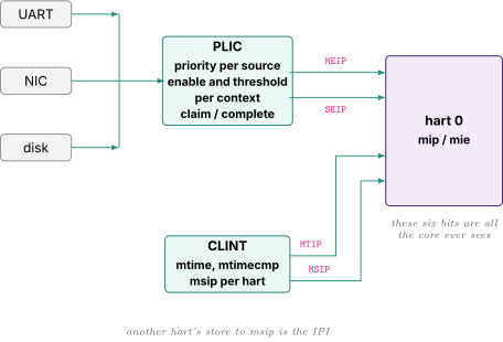
7.4 Why the AIA exists
The PLIC is simple and it does not scale. Two reasons.
The claim/complete register is a shared memory-mapped location. Every interrupt costs an uncached read and an uncached write to a single device somewhere on the interconnect. On a four-hart embedded part that is fine. On a hundred-hart server it is a hot spot in the fabric and it adds real latency to every interrupt.
It has no story for virtualization. A guest OS running in VS-mode cannot be allowed to write the PLIC's registers directly, because those registers control interrupts belonging to other guests and to the hypervisor. So every guest interrupt claim traps to the hypervisor, which emulates it. That is expensive and it is the standard motivation for hardware interrupt virtualization everywhere.
The Advanced Interrupt Architecture answers both with two new pieces. The IMSIC, incoming message-signalled interrupt controller, is a small per-hart device that receives interrupts as memory writes rather than wires, and holds separate interrupt files for M-mode, S-mode, and each virtual guest. Because a guest's interrupt file is its own address, a device can deliver an interrupt straight into a guest with no hypervisor involvement. The APLIC, advanced platform-level interrupt controller, replaces the PLIC for wired interrupts and can convert a wired interrupt into an MSI write to the appropriate IMSIC.
Arm's equivalent lineage is GICv2 to GICv3 to GICv4, and the motivations are strikingly parallel: message-signalled interrupts for scaling, and direct injection into guests for virtualization. Saying that the two architectures independently arrived at the same answer is a good way to show you understand the forces rather than the acronyms.
7.5 The Debug Specification
Debug is a separate RISC-V specification and it defines real hardware you have to build. Given the reader's DFT and silicon-debug background, this is a section where a little vocabulary goes a long way. DFT and Silicon Debug is the general treatment.
The structure is a chain. A Debug Transport Module, usually a JTAG TAP, is the physical connection to the outside world. It masters a bus called the Debug Module Interface, on which sits one or more Debug Modules. A DM controls one or more harts. The DMI uses between 7 and 32 address bits and each address is a single 32-bit register.
Debug Mode is effectively a fourth privilege mode, more privileged than M, that a hart enters when halted. Two CSRs exist only for it: dcsr, the debug control and status register, and dpc, holding the PC where execution will resume. dcsr contains bits ebreakm, ebreaks, and ebreaku that decide, per privilege mode, whether an EBREAK instruction enters Debug Mode or raises an ordinary breakpoint exception. That is how a debugger makes software breakpoints work. Patch an EBREAK into the code and set the corresponding bit.
There are three ways for a debugger to get work done, in increasing order of capability and hardware cost.
Abstract commands are the minimum. The command register plus data0 and up implement a small fixed set of operations, principally "read or write a general-purpose register." An implementation can service these with dedicated hardware and never disturb the hart's pipeline.
The Program Buffer, progbuf0 and up, is a small array of instruction words that the halted hart can be made to execute. Anything not covered by an abstract command, reading a CSR, reading memory through the hart's own MMU, is done by writing a short instruction sequence into the buffer and running it. Enormously flexible, and it means the hart must be able to fetch from the debug module.
System Bus Access lets the debugger read and write memory through the debug module directly, without using a hart at all. That is what lets you inspect memory while every hart is running, or when a hart is wedged.
Separately, the Trigger Module provides hardware watchpoints. tselect picks a trigger and tdata1 through tdata3 configure it. The main trigger type, currently mcontrol6, matches on an address or a data value for loads, stores, or instruction fetches, with a mode mask for which privilege levels it applies to. Other types include instruction counters and trap-on-exception triggers. This is the RISC-V equivalent of the breakpoint and watchpoint units that DFT and Silicon Debug covers generically, and the design question it raises is familiar: how many comparators, how wide, and do they sit in the load/store path where they cost timing.
Instruction trace is yet another specification family, covering branch-trace and full-instruction-trace encoders. I know less about the current state of those documents than about the debug module itself and would say so rather than guess.
08.Part 8, interview questions with model answers
Seventeen questions, each with an answer written the way you would actually say it out loud, the follow-up the interviewer will reach for next, and where relevant the trap.
8.1 Why are the immediate bits scrambled across the RISC-V instruction formats?
Answer. The scrambling is a consequence rather than a goal, and it comes from three constraints stacked on each other.
The first constraint is that the register fields never move. rs1 is always at bits 19:15, rs2 at 24:20, rd at 11:7, in every format that has them. That is because the register file read has to start at the top of the decode cycle, with no logic between the instruction bits and the address decoder. If the position depended on the opcode you would have an opcode decode plus a mux in front of an SRAM read, which is easily 60 to 80 picoseconds of a 333 picosecond cycle at 3 gigahertz.
Once the register fields are nailed down, the immediate has to live in the leftovers, and the leftovers differ by format. A store has no rd, so bits 11:7 are free. A jump has no source registers at all.
The second constraint is that the sign bit is always instruction bit 31. Every immediate is sign-extended, and on a 64-bit machine that is up to 52 copies of one bit. Pinning the source of that fanout to a fixed instruction bit means sign extension starts with zero logic in front of it.
The third is that branch and jump offsets are in units of two bytes, so they need a multiply by two, and rather than build a shifter they rotated the encoding so the bits land where a shift would have put them. The spec says that saves roughly a factor of two in immediate mux cost and instruction signal fanout.
The result is that most immediate output bits have exactly one possible source. Only one bit, imm[11], needs a four-way mux. If you count two-input muxes it comes to about 38, against 992 for a design where any immediate bit could come from any instruction bit. More importantly the depth is two levels instead of five.
Follow-up: "who pays for it?" Software, once. The assembler, the disassembler, and the linker relocations have to implement the scramble, and a human reading a hex dump has to reassemble a branch offset from four pieces. That is a one-time cost borne by a handful of tool authors against a per-chip saving borne by every implementer.
The trap. Do not stop at "the sign bit is at bit 31." That is one of three constraints and it is the one everybody knows. The fixed register fields are the cause. The sign bit and the no-shifter rule are refinements.
8.2 Why does RISC-V have no condition codes, and what does that cost?
Answer. A flags register is architectural state that a very large fraction of instructions write, and that creates three problems in a high-performance implementation.
It is a serialization point unless you rename it, because every write creates a write-after-write dependency. So Arm and x86 implementations do rename the flags, which is extra rename ports, extra physical storage, and extra misprediction recovery. RISC-V does not build any of that.
Partial writes are worse. On x86, inc writes some flags and leaves carry alone, so a later reader depends on two producers and the hardware has to merge them. That is a documented stall source. With no flags there is no merge.
And it saves an instruction in the common case, because blt x1, x2, target is one instruction where Arm needs subs then b.lt.
The costs are real and I would name them. The branch now contains a 64-bit magnitude comparison in its resolution path, where Arm reads a precomputed bit. You cannot compare once and branch several times. And the biggest one is that RISC-V originally had no conditional select, which matters for unpredictable branches and for constant-time cryptographic code where a data-dependent branch is a side channel. The Zicond extension eventually added czero.eqz and czero.nez, and Zicond is mandatory in RVA23. The ISA had to add the capability back.
Follow-up: "so was it a mistake?" No, but it was a trade whose cost showed up later and in a specific place. The core argument, that flags are shared state that every instruction writes, holds. The gap was that a select is not really about flags at all, and the fix was a two-instruction primitive that does not reintroduce a flags register.
8.3 Walk me through an Sv39 page-table walk for virtual address 0x8004_2AB8.
Answer. Sv39 is a 39-bit virtual address, three levels, nine index bits each, twelve bits of page offset. That falls straight out of the geometry: a 4 KiB page needs 12 bits of offset, a page table is one page of 8-byte entries so it has 512 entries and needs 9 index bits, and three levels gives 39.
Decomposing this address, the offset is the low twelve bits, 0xAB8. VPN[0] is bits 20:12, which comes out to 66. VPN[1] is bits 29:21, which is 0. VPN[2] is bits 38:30, which is 2.
satp gives the root table. Say satp.PPN is 0x80200, so the root table is at 0x8020_0000. Level two reads the PTE at 0x8020_0000 + 2 * 8, which is 0x8020_0010. If that entry has V set and R, W, and X all clear, it is a pointer, and the PPN in bits 53:10 gives the next table.
Level one reads at that table plus 0 * 8. Level zero reads at the next table plus 66 * 8, which is +528, so 0x8020_2210. If that entry has R set it is a leaf, and the final physical address is its PPN shifted left twelve, plus the untranslated 0xAB8.
Three dependent memory accesses, each of which can itself miss.
Follow-up: "how do you know a PTE is a leaf?" If V is set and R, W, and X are all zero it is a pointer to the next level. Anything else with V set is a leaf. And R = 0 with W = 1 is a reserved encoding that faults, because writable-but-not-readable is meaningless.
Follow-up: "what if you stop early?" Then you have a superpage. Stopping at level one is 2 MiB, at level two is 1 GiB. The constraint is that the unused low PPN fields must be zero, so a 2 MiB leaf needs PPN[0] == 0. If they are not zero the hardware raises a misaligned superpage fault rather than doing something plausible.
8.4 Under RVWMO, can this message-passing code fail? Fix it.
(The interviewer writes the four-instruction example from 4.1.)
Answer. Yes, and for two independent reasons, which is the thing worth saying because most people find one.
On the producer, nothing in preserved program order orders two stores to different addresses, so the flag store can become visible before the data store. Physically that is an out-of-order store buffer, or a flag line already in modified state while the data line is being fetched.
On the consumer, nothing orders two loads to different addresses either, and the branch does not help. A control dependency is preserved only when the second operation is a store. A control dependency ending in a load is explicitly not preserved, because forbidding speculation past a branch to a load would forbid the most important thing a front end does. So the consumer can issue the data load before the flag load has returned.
The fix needs a fence on each side. fence w, w between the producer's two stores, and fence r, r between the consumer's two loads. Fixing only one side leaves it broken.
Follow-up: "would fence rw, rw work?" Yes, and it is stronger than needed on both sides. The narrower fences let an implementation, for instance, order the store buffer without stalling loads. On a simple machine every fence is a full drain and the distinction buys nothing, but the encoding lets an aggressive machine exploit it.
Follow-up: "what if the consumer did a dependent load instead of a branch?" If the data load's address were computed from the flag load's value, that is a syntactic address dependency and rule 9 preserves it, so the consumer side would be safe without a fence. That is exactly the read-copy-update idiom. The producer side still needs its fence.
The trap. Answering "the branch orders them" is the standard wrong answer and it is wrong on both Arm and RISC-V.
8.5 What is a syntactic dependency, and why does the memory model use that rather than a real one?
Answer. A syntactic dependency is defined on the register dataflow written in the program, not on whether the value actually matters. If a load writes a0, and xor a1, a0, a0 writes a1, and a1 is used to compute the address of a second load, then RVWMO says the second load is ordered after the first, even though a0 XOR a0 is zero regardless of what was loaded.
The reason for the syntactic definition is that a semantic one is unusable. It would require the model to say exactly which value-flow reasoning a compiler or a processor is allowed to see through, and there is no principled place to draw that line. A syntactic definition is mechanically checkable by a tool or by a person reading the code.
The hardware consequence is the interesting part. An implementation that optimizes away a false dependency must not thereby break the ordering. If your renamer recognizes xor a1, a0, a0 and produces a zero immediately, you have removed an ordering the architecture promised. Value prediction is the sharper version. Predicting the loaded value and computing the address from the prediction removes the dependency entirely. I would want to check the spec's current discussion of that before claiming a definitive rule, but the tension is real and the spec acknowledges it.
Follow-up: "why do address dependencies get preserved at all?" History. Alpha did not preserve them, so a load whose address came from another load could execute first, which broke pointer chasing so badly that Linux grew a dedicated barrier for it. Every subsequent architecture preserves them, which is why lock-free read-side code works without an explicit barrier.
8.6 Explain vsetvli. What is LMUL and when would you use 8 versus 1?
Answer. vsetvli rd, rs1, e32, m1, ta, ma is a question and an answer in one instruction. rs1 holds the number of elements the program still wants to process, called AVL. The immediate names the element width, the register grouping, and two policy bits. The hardware writes back into rd and into the internal vl register the number of elements it will actually do. Every vector instruction after it operates on exactly vl elements.
The number it returns is bounded by VLMAX = LMUL * VLEN / SEW. If AVL is at most VLMAX you get AVL. If AVL is at least twice VLMAX you get VLMAX. In between, the implementation may return anything from ceil(AVL/2) up to VLMAX, which exists so that nine elements on an eight-wide machine can come back as five and four rather than eight and one, keeping both passes near full.
LMUL is how many physical vector registers are glued into one logical register. LMUL of 8 means one instruction covers eight registers' worth of elements, so eight times the work per instruction, but only four logical registers remain out of thirty-two and a group has to start on a multiple of eight. So the trade is elements per instruction against register pressure. A simple streaming kernel with two inputs and one output wants a large LMUL. A kernel with six live vectors cannot use LMUL of 8 without spilling and should use 1 or 2.
Follow-up: "why do fractional LMULs exist?" For mixed-width code. VLMAX depends only on the ratio LMUL over SEW, so if you widen from 16-bit to 32-bit elements you have to double LMUL to keep the element count matched. Starting the narrow side at LMUL one-half lets the wide side sit at LMUL 1, so no register group is larger than one register and the element counts still line up.
Follow-up: "what happens if I ask for something unsupported?" It does not trap. It sets vtype.vill, zeroes the rest of vtype and vl, and then any vector instruction that depends on vtype raises an illegal instruction. That indirection is what lets software probe for supported configurations by executing a vsetvl and reading vtype back, with no exception handler needed.
8.7 Why is VLEN not encoded in the instruction, and what does that buy the hardware?
Answer. Two things, one for software and a bigger one for hardware.
For software, one binary runs on a 128-bit machine and a 1024-bit machine with no recompilation and no separate epilogue loop, because the tail is handled by the same instructions with a smaller vl. Contrast x86, where SSE to AVX to AVX2 to AVX-512 each needed a new register file, new opcodes, and in the last case a new prefix and new mask registers.
For hardware, the important consequence is that VLEN is not the same thing as the datapath width. An implementation can have VLEN of 512 bits and a 128-bit execution datapath, and simply take four cycles per vector instruction. Architecturally nothing changed. From the front end's point of view, one fetch, one decode, one rename, one issue and one retire now cover four times the arithmetic.
That is the classical temporal vector machine, and it is why this model fits area-constrained designs in a way fixed-width SIMD does not. Fetch, decode, rename and issue are a large fraction of a core's power, so amortizing them over four times the work is a direct energy-per-operation win, not just an instruction-count win. Then when you want more throughput you widen the datapath and the same binaries run faster.
Follow-up: "so is performance portable?" No, and that is the honest cost. Two conformant machines with the same VLEN can differ by four times in vector throughput because one has a wider datapath and one takes more passes. The binary is portable. The tuning is not. Library authors have found that harder than the marketing suggests.
8.8 We want a custom instruction for a hot kernel. Walk me through what you would do.
Answer. I would start before the instruction, with the arithmetic, because that decides whether the rest is worth doing.
Profile first and get the fraction of runtime the kernel actually takes. If it is 30 percent and the instruction makes that part four times faster, Amdahl gives one over 0.70 plus 0.075, which is a 29 percent end-to-end speedup, and even an infinitely fast instruction caps at 43 percent. That is probably not worth a decoder change, a toolchain change, a verification effort and a kernel patch. If the kernel is 70 percent and the speedup is ten times, you get 2.7 times end to end and it is clearly worth it.
Assuming it passes that bar, seven things.
Pick the encoding. Brownfield, meaning an unused funct7/funct3 combination inside an existing major opcode, if it fits an existing format. That costs almost nothing in decode and risks colliding with a future standard extension. Greenfield, meaning one of the four custom-* major opcodes at 0x0B, 0x2B, 0x5B, 0x7B, if you need a different operand structure or cannot take the collision risk. The last two are also marked for a future RV128 so I would prefer the first two for a long-lived product.
Work out the pipeline impact: latency, pipelined or iterative, whether it needs a stall or scoreboard interlock, whether it needs a new bypass path, whether it fits an existing issue port.
Decide what exceptions it can raise and confirm they are precise. If it touches memory it can page fault, and the machine has to be restartable at that instruction.
Count the architectural state it adds. This is the one that kills proposals. Any new state has to be saved and restored on every context switch and signal delivery, and ptrace, the debugger and the core-dump format all have to know about it. An instruction that only touches existing x registers costs the software stack almost nothing. One with a private accumulator costs it a kernel patch and an ABI change.
Get it through the toolchain, and be honest about which level. .insn hand-encoding works today. Assembler mnemonics are easy. Intrinsics are moderate. Automatic instruction selection by the compiler is hard and often never happens.
Arrange discovery, so software knows it exists. misa only reports single-letter extensions, so realistically that is the device tree or ACPI at boot and a hwprobe-style syscall for user space.
And verify it. It needs a disassembler entry or every trace is unreadable, it needs an independent reference model, and if the arithmetic is at all subtle it wants formal.
Follow-up: "which of those do people forget?" Discovery and context-switch state, in that order. Both are invisible while you are building the RTL and both are blocking before anything ships.
8.9 What breaks in the fetch unit when you turn on the C extension?
Answer. The length decode itself is trivial. If instruction bits 1:0 are anything other than 11 it is a 16-bit instruction, so length is two bits away from the raw fetch data. Everything else is harder.
Instructions become two-byte aligned, so a 32-bit instruction can start at any even address. It can straddle a cache line, which means one instruction needs two cache accesses and a buffer to splice the halves. Worse, it can straddle a page, which means the second half can take a page fault when the first half did not, so the machine has to handle a fault reported partway into an instruction it has not finished fetching. Both cases are rare and both are exactly where front-end bugs live.
Decode width becomes variable. Sixteen bytes might be four 32-bit instructions or eight 16-bit ones or any mixture, so before the real decoders you need length decode and alignment logic to find where each instruction starts, and that is a serial dependency at the head of the front end.
And branch targets can be any even address, so nothing downstream can assume four-byte alignment.
Follow-up: "so would you implement it?" For an embedded core, unambiguously yes, the code-size saving is large and the front end is simple. For a wide out-of-order core it is a real cost and you take it anyway, because instruction cache footprint and fetch bandwidth matter more than the alignment logic. But I would want the alignment path designed and verified early rather than bolted on.
8.10 Explain M, S, and U mode and trap delegation. Why does delegation exist?
Answer. M mode is the only mandatory mode and it is where firmware runs with unrestricted access. S mode is where an OS kernel runs and it controls address translation through satp. U mode is applications. Only three combinations are legal: M alone for a deeply embedded part, M and U with physical memory protection for an embedded part that wants isolation without an MMU, and M, S and U for a Unix-class machine.
By default every trap goes to M mode. On a Unix machine that is wrong, because a user page fault or a syscall is the kernel's business and the kernel is in S mode. Without delegation, every page fault would enter M-mode firmware, which would then manufacture a second synthetic trap down into S mode. That doubles the cost of every syscall and every page fault, and a trap entry on a deep out-of-order machine is a pipeline flush plus a privilege change, so it is on the order of a hundred cycles. Doubling that is not marginal.
Delegation is two bitmaps, medeleg for exceptions and mideleg for interrupts, indexed by cause code. Setting bit 13 of medeleg means a load page fault occurring in S or U mode goes directly to stvec, and the S-mode registers sepc, scause, stval and the SPP, SPIE, SIE bits of sstatus take over from their M-mode counterparts.
Two rules constrain it: a trap is never delegated to a mode less privileged than where it occurred, and traps taken in M mode are never delegated at all.
Follow-up: "walk me through the trap entry sequence." mepc gets the address of the faulting instruction, not the next one, because a page fault is restartable. mcause gets the cause with the top bit indicating interrupt versus exception. mtval gets the faulting address. Then mstatus.MPIE takes the old MIE, MIE is cleared so interrupts are off, MPP records where we came from, and the PC becomes mtvec. MRET reverses all of it, and it also forces MPP back to the least privileged supported mode, which is a hardening measure so a later bug cannot accidentally return to a higher privilege.
8.11 What is the CLINT, what is the PLIC, and why are they two devices?
Answer. Because RISC-V defines only three interrupt sources per privilege level, software, timer and external, and puts everything about how interrupts are generated outside the core. The core just sees mip bits.
The CLINT handles software and timer. It is memory-mapped and has three things. There is a per-hart msip word, where another hart storing 1 into it is the entire inter-processor interrupt mechanism. There is a single free-running mtime counter. And there is a per-hart mtimecmp, where the hardware continuously sets mip.MTIP whenever mtime is at least mtimecmp.
The PLIC handles external interrupts, which is everything else in the system. It has numbered sources with source 0 reserved to mean "none," a priority per source, and per-context enable bitmaps and thresholds, where a context is a hart and privilege level pair. The handshake is claim and complete. Reading the claim register atomically returns the highest-priority pending enabled source and clears its pending bit, and writing that ID back re-arms it.
They are separate because they solve different problems. Timer and IPI are per-hart and need no arbitration, so a trivial memory-mapped device suffices. External interrupts need prioritization, masking, and routing among many harts, which is a much bigger device that nobody wants in a microcontroller.
Follow-up: "why two steps instead of an automatic acknowledge?" The gap between claim and complete is when the handler talks to the device and clears the device's own interrupt condition. If the controller re-armed at claim time, a level-triggered device would immediately re-assert and the handler would spin.
Follow-up: "any gotchas with the timer?" Yes, and it catches everybody. mip.MTIP is read-only and level-driven. Acknowledging the interrupt does not clear it. The only way to clear it is to write a new, larger mtimecmp. A handler that returns without doing that re-enters forever. And on RV32, mtimecmp is two 32-bit stores, so you write all-ones to the high half first to avoid transiently creating a compare value in the past.
8.12 You are building a two-wide in-order RV64 core for a Linux-capable SoC. Which extensions do you implement, and in what order?
Answer. Linux-capable sets the floor. I need I, M, A, Zicsr, Zifencei, S mode with Sv39, and C, which together is roughly RV64IMAC plus supervisor support. F and D if there is any floating point in the workload, which for general-purpose Linux there is, so realistically RV64GC.
Then I would target RVA23 rather than picking piecemeal, because the whole point of a profile is that a distribution can build one binary against it. That pulls in Zba, Zbb, Zbs, Zicond, and the V extension as mandatory.
Order of implementation I would drive by cost and by what unblocks software. I plus Zicsr plus M mode first, because that boots. Then M, then A, because the kernel needs atomics for locks. Then S mode and Sv39, which is the page-table walker and the TLB and is the largest single chunk of work. Then C, and I would want the fetch alignment path designed early rather than retrofitted, because that is where the bugs are. Then F and D. Then the bit-manipulation set, which is genuinely cheap. Zba's shift-add instructions and Zbb's count-leading-zeros and byte-reverse are small combinational blocks that fit the existing R-type format, so the decoder barely changes.
V last and largest, and I would want an honest conversation about whether it is in scope, because it is a second 32-entry register file, a vsetvl mechanism, vstart restartability, and a load/store unit that handles strided, indexed and segmented accesses. On a two-wide in-order core the sensible design is a modest VLEN with a datapath narrower than VLEN, taking multiple passes per instruction, which gets the front-end amortization benefit without the area.
Follow-up: "what would you leave out?" The hypervisor extension unless virtualization is a product requirement. Zbc carry-less multiply, unless there is a cryptographic workload, since it is optional in RVA23. And I would think hard about whether Zicond is worth it on an in-order core, since the branch misprediction penalty that motivates branchless code is much smaller there, though it is mandatory in the profile so the answer is that I implement it because the profile says so.
8.13 How does LR/SC differ from compare-and-swap, and what does the forward-progress guarantee demand of your hardware?
Answer. Compare-and-swap is a single instruction that atomically compares a memory location against an expected value and writes a new one if they match. LR/SC is a pair. The load-reserved reads the location and establishes a reservation, and the store-conditional writes only if the reservation is still intact, returning zero on success and nonzero on failure.
The practical difference is that LR/SC composes. You can compute anything you like between the two, so you can build compare-and-swap, fetch-and-add, or an arbitrary read-modify-write, from one primitive. Compare-and-swap also has the ABA problem, where a value changes and changes back and the comparison succeeds wrongly. LR/SC does not, because the reservation is broken by any intervening write regardless of value.
The hardware obligation is the interesting half. The spec defines a constrained LR/SC loop: at most sixteen instructions laid out sequentially, containing between the LR and SC only base-I instructions and no loads, stores, backward jumps, taken backward branches, JALR, FENCE or SYSTEM instructions. For such a loop the execution environment must guarantee eventual progress, meaning eventually either this hart's SC succeeds or some other hart or device writes the reservation set.
That constrains the design. Your reservation mechanism must not be starvable indefinitely by another hart's traffic, which usually means the coherence protocol cannot allow a line to be stolen away from a hart forever right after it takes a reservation. Some designs give a hart a short window of guaranteed ownership after LR. The sixteen-instruction limit exists precisely so the hardware can bound how long a reservation has to be honored.
Follow-up: "what is a reservation set?" It contains at least the addressed word but may be larger, and how much larger is implementation-defined. That has a visible software consequence. On an implementation with a coarse reservation set, two threads doing LR/SC on adjacent words in the same granule can knock each other's reservations down and, in a badly written loop, livelock. It is the atomics version of false sharing.
8.14 What does the Debug Specification require you to build into the core?
Answer. More than people expect, and it is real RTL rather than a software feature.
The structure is a chain. A Debug Transport Module, usually a JTAG TAP, masters a Debug Module Interface bus, on which sits a Debug Module that controls one or more harts. The DM can halt and resume harts through dmcontrol.
In the core itself, Debug Mode is effectively a fourth privilege level above M. It needs two CSRs that exist only for it, dcsr and dpc, and dcsr carries ebreakm, ebreaks and ebreaku bits that decide per privilege mode whether an EBREAK enters Debug Mode or raises an ordinary breakpoint exception. That is the mechanism software breakpoints ride on.
Then there are three ways the debugger gets work done, at increasing hardware cost. Abstract commands are a small fixed set, principally read and write a general-purpose register, which an implementation can service with dedicated hardware. The Program Buffer is a small array of instruction words that the halted hart executes, which is how you read a CSR or read memory through the hart's own MMU, and it means the hart must be able to fetch from the debug module. System Bus Access lets the debugger read and write memory without using a hart at all, which is what saves you when a hart is wedged.
Separately, the Trigger Module gives hardware watchpoints. tselect picks a trigger and tdata1 through tdata3 configure it, and the main type matches address or data for loads, stores or fetches with a privilege-mode mask.
Follow-up: "what is the design cost of the triggers?" The same cost as any watchpoint unit: comparators sitting in the load/store address path, which is usually timing-critical. How many, how wide, and whether they compare the virtual or the physical address are all real decisions, and they interact with the pipeline stage where the address is available.
How to handle this if debug is not your area. Say what you know about the structure, then pivot to what you have done. Post-silicon debug hooks and trigger logic are the same discipline whatever the ISA calls them.
8.15 Compare RISC-V's vector extension to Arm SVE.
Answer. Both are vector-length agnostic, which is the main thing, and both exist because fixed-width SIMD forced an ISA extension every time hardware got wider.
The structural difference is where the "how many elements" state lives. RVV puts it in architectural CSRs, vl and vtype, that one vsetvl instruction sets and every subsequent vector instruction implicitly reads. SVE puts it in a predicate register produced by something like whilelt and consumed as an explicit operand.
Each choice has a cost. RVV's implicit state means a renaming machine has to track vtype and vl as dependencies, and a vsetvl acts as a serialization point for the vector instructions after it. SVE's explicit predicates cost encoding bits on every instruction but keep the dependency visible. SVE also encodes element width in the opcode, so it needs more opcodes but avoids RVV's mode-switch dependency. And RVV has LMUL, run-time register grouping, which SVE has no analogue for at all. SVE has sixteen predicate registers where RVV has exactly one mask register, v0.
On widths, SVE is 128 to 2048 bits in 128-bit steps. RVV's VLEN is a power of two up to 2 to the 16.
The trap, and how I would handle it. I would be explicit that I have read the SVE specification rather than built against it, and that the comparison above is the level I am confident at. If pushed into SVE2 or SME I would say I do not know rather than guess. Getting caught inventing a detail about a competitor's ISA is much worse than the gap it covers.
8.16 RISC-V is a RISC ISA, so it must be simpler to implement than x86. Do you agree?
Answer. For a small core, unambiguously yes, and the reasons are concrete: fixed 32-bit encodings, three-address instructions with fixed register field positions, no condition codes, no addressing modes beyond register plus immediate, no instruction that both computes and accesses memory.
For a high-performance core the gap narrows a great deal, and I would rather give the honest version. Once you are building a wide out-of-order machine, the expensive parts are the branch predictor, the rename and scheduling machinery, the load/store queue, the cache hierarchy and the coherence protocol, and essentially none of that gets easier because the decoder is simpler. x86's decoder is genuinely awful and genuinely expensive, but it is a fixed cost that gets amortized by a micro-op cache, and it is not the reason a modern core is hard.
RISC-V also brings its own hard problems that x86 does not have. The compressed extension makes instructions two-byte aligned, so a 32-bit instruction can straddle a cache line or a page, which is real front-end complexity. The weak memory model shifts effort from hardware to verification, because you now have to prove your load/store queue implements exactly the preserved-program-order rules rather than the much simpler TSO invariant. SFENCE.VMA is hart-local rather than broadcasting, so TLB shootdown is a software protocol you have to get right. And the modularity means your verification matrix has more axes.
So the fair statement is that RISC-V removes a large fixed cost at the front of the pipeline and does not change the cost of the parts that dominate a high-performance design.
Follow-up: "then why does anyone care?" Licensing and extensibility, mostly, plus the ability to add custom instructions without negotiating with an IP vendor. Those are business and roadmap advantages rather than microarchitectural ones, and I think it is more credible to say that than to claim a performance-per-watt advantage falls out of the ISA.
8.17 If RISC-V is modular, why does RVA23 exist?
Answer. Because modularity and a software ecosystem pull in opposite directions, and the community had to build a second mechanism to contain the first.
Modularity is exactly right for embedded. A microcontroller can implement RV32I alone, about forty instructions, no CSRs, no multiplier, no MMU, and it is a legal RISC-V machine. That is a genuine advantage over Arm, where even the smallest profile carries more mandatory baggage.
It is a disaster for a Linux distribution. If every vendor picks a different subset there is no single binary that runs everywhere, and either the distribution ships many builds or it targets the intersection, which is the lowest common denominator. That is the fragmentation risk, and RISC-V had it far worse than any prior architecture because the extension space is far larger.
A profile is a named bundle that says "if you claim this, you implement all of these." RVA23U64 is the current application-class one, and the headline change from RVA22 is that the V extension became mandatory, along with Zicond and the Zba/Zbb/Zbs bit-manipulation set. Zbc stayed optional.
Follow-up: "does that not defeat the point?" It constrains one segment, not the architecture. Embedded parts do not claim RVA23 and are free to be as small as they like. What the profile does is create a stable target for the segment that needs one. I would also say that making V mandatory is a big commitment to force on every application-class implementer, since a vector unit is a large area and verification cost, and it is a bet that the software ecosystem needs it more than small implementers need to skip it.
09.Part 10, check yourself
Answer out loud, in full sentences, as an interviewer would hear them. If you cannot, reread the section named.
- Hand-decode
0xFEC30293into its fields and say what the instruction does. (1.1) - Why is the register count 32 and not 16 or 64? Give the arithmetic. (2.1)
- Give five things
x0buys you that would otherwise need their own opcodes. (2.1) - Why do
rs1,rs2, andrdoccupy fixed bit positions in every format, and what would it cost if they did not? Put a number on it. (2.2) - State all three constraints that produce the immediate scrambling, and count the two-input muxes the design actually needs versus a full crossbar. (2.4)
- Encode
beq x5, x6, -20by hand, showing where each immediate bit goes. (2.3) - Give three hardware reasons RISC-V omitted condition codes, and then three things that omission costs. What did
Zicondadd back and why? (2.5) - Explain the
Winstructions in RV64I and why the result is sign-extended rather than zero-extended. (2.7) - Name the four custom opcodes, say which two carry a caveat, and explain brownfield versus greenfield. (3.4)
- Walk the seven-item checklist for adding a custom instruction. Which two items kill most proposals? (3.5)
- A kernel is 30 percent of runtime and a custom instruction makes it 4 faster. What is the end-to-end speedup, and what is the ceiling at infinite speedup? (3.6)
- Write the message-passing litmus test and give both reasons it can fail under RVWMO. Fix it with the narrowest fences that work. (4.1)
- Group the thirteen preserved-program-order rules into four families and state what each family is for. Which rule explains why a branch does not order two loads? (4.3)
- What is a syntactic dependency, why is the definition syntactic rather than semantic, and what does that demand of a renamer that wants to break false dependencies? (4.4)
- Give the eight
FENCEbits and say whatfence rw, wmeans. What isFENCE.TSOand why does it exist? (4.5) - Write the release-then-acquire pair that RCpc leaves unordered and RCsc orders. Which preserved-program-order rule closes the gap, and what does
Zalasradd that the base model lacked? (4.6) - What obligation does the constrained
LR/SCforward-progress guarantee place on your coherence protocol? (4.6) - Which rows of the ordering table differ between RVWMO and Arm A64? Which differ between RVWMO and x86-TSO? (4.7)
- Derive Sv39's from the page size and the entry size. Then walk
0x8004_2AB8to a physical address. (5.5) - How does the hardware distinguish a pointer PTE from a leaf PTE, and what makes a superpage mapping fault? (5.5, 5.6)
- Why does trap delegation exist, and what does a syscall cost without it? (5.4)
- Why is
SFENCE.VMAhart-local, and what does that force software to do that Arm software does not? (5.6) - Decode CSR numbers
0x300and0xC00, and say what the permission logic learns from bits 11:10 and 9:8 without consulting a table. (5.2) - Compute VLMAX for VLEN = 256 across SEW and LMUL . (6.2)
- State the three rules turning AVL into
vl, and explain why the middle case is a range rather than a value. (6.3) - Why do fractional LMULs exist? Work a widening example. (6.4)
- What are
vtaandvma, and why would an implementation prefer agnostic? (6.5) - Explain why VLEN and datapath width are different things, and what that buys a small core. (6.6)
- Where does the "how many elements" state live in RVV versus SVE, and what does each choice cost? (6.7)
- Why is
mip.MTIPstill set after your timer handler returns? (7.2) - Describe the PLIC claim/complete handshake and say why it is two steps. (7.3)
- Name the two problems the AIA exists to solve. (7.4)
- Name the three ways a debugger gets work done through a Debug Module, in increasing order of hardware cost. (7.5)
10.Part 11, related notes
- CPU Foundations Pipeline and Hazards for the pipeline that the decode-timing argument in 2.2 is about, and for the precise-exception requirement that Part 3's custom-instruction checklist leans on
- Virtual Memory and Memory Ordering for why translation exists at all, for the TLB, for the consistency-model vocabulary that Part 4 assumes, and for the comparison table that holds the vault's only prior RVWMO mention
- Load Store and Memory Ordering for the load queue and store buffer that RVWMO's rules actually constrain, and for the same-address coherence check that preserved-program-order rule 2 demands
- Front End and Branch Prediction for the fetch alignment machinery that the C extension forces, and for why control dependencies to loads are deliberately not preserved
- Execution Units for ports, bypass networks, and the SIMD material that Part 6 contrasts against
- Out of Order Execution for renaming, which is where
x0, the absence of condition codes, and LMUL register grouping all show up as design consequences - Cache Coherence Protocols and Interconnect and AMBA for what a weak memory model lets the interconnect stop guaranteeing
- Security Side Channels and Speculation for why one
satprather than two table base registers has security consequences - Power Fundamentals and Clock Gating for the front-end energy that vector-length agnostic execution amortizes, and for the sequencing discipline that maps onto trap entry and exit
- Verification Methodology for where formal fits on decoders, CSR permission logic, and memory-model litmus tests
- DFT and Silicon Debug for the general treatment of the breakpoint, watchpoint, and trace hardware that 7.5 specializes
- SoC Integration and Interfaces for where a PLIC or an APLIC sits in a real SoC
- SRAM Arrays and ECC and Reliability Aging and Variation for the vector register file and TLB as arrays with reliability requirements
- Performance Modeling for where the profile that justifies a custom instruction comes from
- Programming and Tooling for the toolchain end of Part 3's checklist
- RISC-V: A Modern Open ISA for the vault's survey of the base ISA and the extension list
- ARM A64: The Mobile and Server Workhorse for the architecture every comparison in this note is drawn against
- Privilege, Exceptions, and System Instructions for the vault's cross-ISA treatment of privilege and exceptions
- Vector and SIMD Programming Models for the vault's vector chapter, including its own VLMAX worked examples
- Project: A Two-Pass Assembler for RV32IMC for the project that makes Part 2 permanent by forcing you to implement the immediate scramble both ways
- Project: Building a 5-Stage Pipelined RV32IM CPU in Chisel for a working core and a genuine Chisel data point
- Lab: Verification and Cycle-Accurate Simulation for
riscv-tests, Verilator, andriscv-formal - Case Study: Open-Source In-Order Cores and Case Study: BOOM (Berkeley Out-of-Order Machine) for real RTL implementing everything above