CXL and Coherent Memory Expansion
September 8, 2026133 min readadvanced
Do not start from the acronym. Start from two engineers, in two different buildings, each with a problem that has nothing obvious to do with the other. The value of this note is almost entirely in feeling…
01.Part 1, two problems that look unrelated, and one answer
Do not start from the acronym. Start from two engineers, in two different buildings, each with a problem that has nothing obvious to do with the other. The value of this note is almost entirely in feeling those two problems before meeting the mechanism, because CXL only makes sense as the answer to a question, and the question is what interviewers actually probe.
1.1 The first problem, a server that cannot hold enough memory
Build a concrete machine. One socket. Eight DDR5-4800 memory channels, which is a real and public configuration point. One DIMM per channel, because that is what runs at full speed. 64 GB registered DIMMs.
Capacity is GB. Bandwidth is the data rate times the bus width per channel, times the channel count,
Now the workload arrives and it wants one terabyte. Not because the programmer was careless, but because it is an in-memory database, or a recommendation model's embedding tables, or a virtual-machine host that has been asked to pack more tenants. There are four things you can do and every one of them is bad in a specific, countable way.
Buy denser DIMMs. Move from 64 GB to 128 GB parts. This works, and it is the first thing anybody tries. The cost is that the price per gigabyte at the top density point is materially higher than at the volume point, and it moves with the memory market rather than with physics. That is a purchasing fact, not an engineering one, and it is worth saying so plainly rather than pretending it is a law.
Put two DIMMs on each channel. The slots exist. Capacity doubles to 1 TB and you are done. Except that hanging a second module on a channel adds a second electrical load to a bus already running at 4800 megatransfers per second, and platforms respond by derating the supported data rate at two DIMMs per channel. The exact derate is platform and vendor specific and I will not invent a number, but the direction is not in doubt and it is the whole reason the option is unattractive. You bought capacity by spending bandwidth, on a machine whose bandwidth was already the scarce thing.
Buy a second socket. A second socket brings eight more channels, so 512 more gigabytes. It also brings a second processor's worth of cores you did not want, a second processor's worth of licence cost in software that charges per socket, a second processor's power, and a non-uniform memory architecture where half your memory is now a socket hop away. You wanted 512 GB and you bought a computer.
Page to storage. An NVMe SSD is enormous and cheap. Its access latency is in the region of tens of microseconds. Local DRAM is in the region of eighty nanoseconds. That is a factor of roughly a thousand, and Part 9 will show exactly what a factor of a thousand does to a program that was not written to expect it.
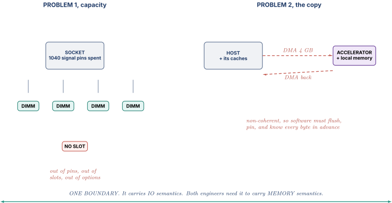
So the honest statement of the first problem is this. A socket's memory capacity is bounded by the number of DIMM slots you can hang off it, and that number is bounded by pins and by signal integrity, not by anything you can buy your way out of. Which brings the argument to the number that actually explains why a serial link is the answer.
1.2 The pin budget, counted, which is the real constraint
A processor package has a finite number of signal pins. Everything the socket does (memory, IO, socket-to-socket links, power delivery) competes for them, and power and ground take a large majority of the total before any signal gets a pin at all.
Count what a DDR5 channel costs, and count it for DDR5 specifically rather than reusing the DDR4 number, because the two differ in a way that matters here. A DDR4 channel was one 64-bit bus with 8 ECC bits bolted on the side, 72 DQ pins in total. DDR5 splits the same 64 data bits into two independent 32-bit sub-channels, and each sub-channel carries its own 8 ECC bits. So the arithmetic is DQ pins, not 72. The data width did not change but the ECC width doubled, because two independently commanded sub-channels each need their own protection.
Now add everything that travels with those 80 bits. Differential strobe pairs, roughly one pair per byte lane, so about 20 pins. A command and address bus per sub-channel, seven bits each. A differential clock pair per sub-channel. Chip selects per rank per sub-channel. Then the housekeeping signals (reset, alert, mirroring, and so on). The count for one channel lands somewhere around 130 signal pins. The exact figure depends on the DIMM type, the rank count, and whether ECC is present, so treat 130 as an order-of-magnitude figure rather than a datasheet value. Eight channels is therefore roughly 1040 signal pins, and those 1040 pins deliver 307 GB/s, shared between reads and writes, because a DDR bus is half duplex and every turnaround costs a bubble, as DRAM Controllers JEDEC and DFI works out in detail.
Now count a PCIe Gen5 x16 link. Each lane is two differential pairs, one per direction, so four signal pins per lane, 64 signal pins for the whole link. From the table in Part 7.1 of SoC Integration and Interfaces, Gen5 delivers 3.94 GB/s per lane per direction, so the link carries 63 GB/s each way, simultaneously, because a serial link is full duplex with dedicated wires per direction.
Compare them fairly and the answer is still decisive. If your traffic is one-directional, a serial pin is more than three times better than a parallel pin. If your traffic is symmetric, so that the full-duplex link's two directions are both busy, it is more than six times better. Either way the conclusion is the same and it is the structural fact underneath this entire note.
Per pin, a serial link carries several times more bandwidth than a parallel memory bus, and pins are the resource the socket is actually short of. That is why every high-bandwidth interface in a modern system except memory itself went serial two decades ago, and it is why the idea of putting memory behind a serial link is not perverse. It is the obvious thing to try once you have counted pins.
There is a price and it is latency, which Part 9 pays in full and in public.
1.3 The second problem, the copy
Different building, different engineer. She has an accelerator sitting on a PCIe Gen5 x16 slot. It might be a field-programmable part, a machine-learning engine, or a compression or cryptography offload, and the category does not matter. Her problem is not capacity. Her problem is that her device cannot touch host memory.
Follow what actually has to happen today, from SoC Integration and Interfaces Part 6.3. The host allocates a buffer. The driver pins it so the operating system cannot move it. If the device is not IO-coherent the driver must clean every cache line of that buffer to memory, because the fresh data is sitting dirty in the CPU's caches and DRAM holds stale bytes. It builds a descriptor, rings a doorbell, and the device's DMA engine reads the buffer over PCIe into its own memory. The device computes. The device DMAs results back. The driver invalidates the destination buffer's lines so the CPU does not read stale copies. An interrupt fires and software carries on.
Price the copy two ways, because both prices matter and only one of them is usually mentioned.
The bandwidth price. Say the working set is 4 GB. A Gen5 x16 link is 63 GB/s in theory, and sustained large DMA on a real platform is lower. Call it 50 GB/s and treat that as an illustration, since achieved DMA throughput varies widely with the platform, the descriptor size, and the IOMMU configuration. Then
Eighty milliseconds before the accelerator has done one useful operation, and roughly as much again to bring results back. If the kernel itself takes 20 ms, you have built a machine that spends 89 percent of its time moving data past itself.
The waste price, which is worse. Suppose the kernel is sparse. It touches one million scattered 64-byte lines out of that 4 GB structure. Useful data is MB. You copied 4 GB. You moved sixty-four times more data than the computation needed, because a bulk copy is the only tool available and a bulk copy cannot know which bytes will be touched.
The alternative is to have the device issue a separate PCIe read for each 64-byte line it actually wants, and that trades one disaster for another. A device-initiated read of host memory is a non-posted transaction whose completion has to come all the way back, and public measurements of that round trip on real platforms land in the region of one to two microseconds with wide variance. Even with 64 reads in flight,
and the device has burned its entire outstanding-transaction budget doing it.
The semantic price, which nobody mentions and which is the actual killer. Because the copy is not coherent, software must know in advance exactly which bytes the device will touch. Fine-grained sharing is impossible. Consider the smallest possible cooperation, a 64-byte descriptor that the host writes and the device polls. Without coherence, the device must DMA-read that descriptor on every poll, and the host must push its write out of its caches every time it updates one. Poll every microsecond across a 100-microsecond idle window and that is a hundred round trips to discover nothing changed. With coherence, the device caches the line, sits on it, and the host's eventual write triggers exactly one invalidation. One hundred transactions become one.
1.4 The two problems are the same problem
Set them side by side.
The first engineer has memory she cannot attach because the socket is out of pins. The second has memory she cannot reach because it is on the wrong side of a boundary that does not carry coherence.
Both are the same statement. The boundary between the processor and everything else carries IO semantics, and what both engineers need it to carry is memory semantics. IO semantics means explicit transfers, ownership by convention, software-managed consistency, and bulk granularity. Memory semantics means load and store at cache-line granularity, with hardware maintaining a single coherent view.
That is what Compute Express Link is. One sentence, and it is the sentence to open an interview answer with:
CXL is a set of protocols that carry cache-coherent memory semantics over a PCIe physical link, so that memory can live on the far side of a serial interface and still be loaded from and stored to like local DRAM.
Everything else in this note is mechanism. Three protocols in Parts 3 to 5, three device types in Part 6, one coherence-optimisation model in Part 7, a fabric in Part 8, an honest accounting of what it costs in Part 9, and in Part 10 the comparison to the coherence you already know, which is where the interview actually goes.
02.Part 2, riding on PCIe, and exactly what that buys and costs
2.1 The alternative, priced, so the decision looks like a decision
Suppose you set out to build a coherent memory interface from scratch. You would need a differential SerDes running at tens of gigabits per lane, equalisation to fight the channel, clock and data recovery, a link training state machine, a lane-reversal and polarity-inversion scheme, an error model, a connector, a mechanical form factor, board design rules, a retimer ecosystem for long channels, compliance test equipment, and interoperability plugfests. Part 7 of SoC Integration and Interfaces describes what most of those things are. The point here is how many of them there are.
Every one of those is years of work and, more damagingly, every one is a place where a device from vendor B fails to work with a host from vendor A. An interconnect standard's real product is not a protocol. It is an ecosystem in which parts from different companies plug together, and ecosystems take a decade to build.
So CXL made the decision that in hindsight looks obvious and at the time was the entire bet. Do not build a physical layer. Use the one that already exists in every server on earth. A CXL link is electrically a PCIe link. Same lanes, same signalling, same connector, same slot, same retimers, same cables, same test equipment, same board rules, same form factors including the EDSFF add-in-card shapes the storage industry already standardised.
Say that in an interview as a design judgement rather than a fact and it lands better: the physical layer is where the ecosystem cost is, and reusing it is what let a coherence protocol reach volume in a few years instead of a decade.
2.2 How a PCIe link becomes a CXL link
Here is the part that surprises people, and it is a good small answer to have ready because it shows you have read past the marketing.
A CXL link starts life as a PCIe link and negotiates itself into CXL mode during link training. PCIe's training sequences include ordered sets with vendor-defined bit fields reserved for exactly this purpose. The mechanism is generally referred to as alternate protocol negotiation, and the CXL and PCIe worlds call the port that supports it a Flex Bus port.
Here is the sequence, described at the level a logic designer needs and hedged where the details are specification territory. The link trains up in the ordinary way at the lowest rate, and while it is there the two ends exchange modified training ordered sets whose vendor-defined bits carry the request and the acknowledgement for CXL mode. Those bits also carry which of the three protocols to enable and which optional latency optimisations both ends support. Once agreed, the physical layer stops sending modified ordered sets, resumes ordinary training, and takes the link up to its full data rate, now running CXL rather than PCIe.
Three consequences that are worth knowing.
Fallback is graceful. Put a CXL device in a plain PCIe slot in a host that does not support CXL, and negotiation simply does not happen. The link comes up as PCIe and the device works as a PCIe device, presenting whatever its CXL.io function exposes. That is a large practical benefit and a good thing to mention.
Protocol selection is a link-time decision, not a per-transaction one. Which protocols run on this link is fixed once the link is up. A device does not decide per request whether to be a memory expander.
The negotiation happens before anything interesting is running, which means a bug in it is a bring-up bug that presents as "the link came up as PCIe and nobody knows why." That is the kind of failure that eats a week in a lab, and knowing where to look for it is worth more than knowing the bit positions.
2.3 The stack, and why CXL.cache and CXL.mem bypass most of PCIe
This is the structural picture and it is the one to be able to draw.
CXL.io rides the full PCIe stack, meaning the PCIe transaction layer producing TLPs, the PCIe data link layer adding sequence numbers and LCRC and running the ACK/NAK retry protocol, exactly as Part 8 of SoC Integration and Interfaces describes. It is PCIe. Nothing new.
CXL.cache and CXL.mem ride a separate, much thinner CXL link layer that shares nothing with PCIe's above the physical layer. Both then feed an arbitration and multiplexing block, universally written ARB/MUX, which interleaves the two streams onto one Flex Bus logical physical layer, which drives the ordinary PCIe electrical layer.
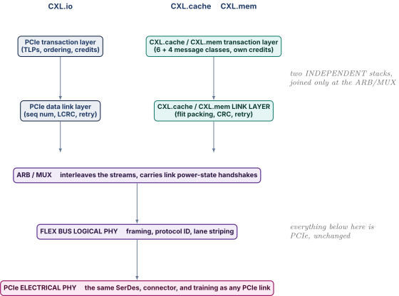
Why the split? Because PCIe's upper layers are the wrong shape for coherence, and being able to say why is a strong signal.
A PCIe TLP header is 12 or 16 bytes, and PCIe's transaction layer carries an elaborate producer-consumer ordering model with posted, non-posted, and completion classes and a set of rules about which may pass which. All of that exists to make a peripheral bus behave sanely for drivers. A coherence message is a different animal. It is small, it is frequently header-only, it has no useful ordering relationship with its neighbours except at the same address, and it lives or dies on latency. Wrapping a 12-byte snoop response in a 16-byte header and then running it through a retry protocol designed for 4-kilobyte payloads would be absurd.
So CXL.cache and CXL.mem get their own link layer optimised for exactly that traffic, and the two stacks meet only where they must, at the point where one set of wires has to carry both.
2.4 The flit, and where the packing pressure comes from
The unit that crosses the wire is a flit, a flow-control unit, the same word and the same concept as Part 3.1 of Interconnect and AMBA.
The original CXL flit, used for the data rates up to 32 GT/s, is 68 bytes, made of a 2-byte protocol identifier, a 64-byte payload, and a 2-byte CRC over the payload. The protocol identifier is what lets the receiver know whether this flit belongs to CXL.io, to CXL.cache/mem, or to the ARB/MUX's own link-management messages, and it carries deliberate redundancy so that a corrupted protocol ID is detectable rather than catastrophic.
The 64-byte payload divides into four slots of 16 bytes. That number is not decoration and it generates the whole packing problem. Work it:
A cache line is 64 bytes. Four slots of 16 bytes is 64 bytes. So a cache line exactly consumes an entire flit's payload, leaving no room in that flit for the header describing it. The header therefore has to travel in a different flit, and the link layer's job every cycle is to choose a legal assignment of pending messages to slots, with some slots carrying headers and some carrying data, subject to rules about which combinations are permitted.
That is a genuinely interesting piece of RTL and it is the same shape as every arbiter in Arbiters FIFOs and CAMs: a set of candidates, a legality mask, a fixed number of resources, and a selection that has to happen every cycle at a link-derived clock. Part 11 comes back to it.
Two further things about flits, both hedged because they are specification territory and the details move.
At the higher data rates introduced with the 64 GT/s generation, CXL adds a 256-byte flit format. The larger flit exists because at those rates the physical layer needs forward error correction (the same PAM4 signalling argument as PCIe Gen6 in Part 7.2 of SoC Integration and Interfaces), and FEC needs a block to work on. The published material also describes a latency-optimised variant of the 256-byte flit whose purpose is precisely to avoid paying the accumulation and decode delay that a large FEC-protected block would otherwise impose on latency-critical coherence traffic. The exact structure of that optimisation is the kind of detail to look up rather than assert.
The general principle is worth more than the format. A coherence protocol cannot afford to wait for a large block to accumulate before it starts processing, and it cannot afford a decode step that adds even one or two nanoseconds on the critical path. Every design decision in the CXL link layer is downstream of that, and if you can only remember one thing about flits, remember that one.
2.5 What riding on PCIe constrains
Reuse is never free and an interviewer will ask what it cost.
A latency floor you cannot design away. A SerDes has to serialise, drive, receive, equalise, recover the clock, and deserialise. Published figures for the round trip from the pin to the digital logic and back land in the region of twenty to twenty-five nanoseconds, varying with whether the two ends share a reference clock. That is before any protocol logic on either side has done anything at all. Part 9 builds the full budget, but this is the term you cannot attack. It is physics plus a standard, and no cleverness in the controller touches it.
A topology inherited from a peripheral bus. PCIe's structure is a tree rooted at a root complex, with switches fanning out and endpoints at the leaves, and configuration cycles flowing downward from a single owner. The early CXL generations lived inside that shape. Part 8 describes how later revisions of the standard grew a genuine switched fabric on top of it, but the starting point was a tree, and trees are a poor match for the "any node talks to any node" pattern that memory sharing eventually wants.
An error model built for a different failure. PCIe's data link layer answers a corrupted packet with a NAK and a retransmission from a retry buffer, which is exactly right when the consumer is a network card and the cost of a retry is microseconds nobody notices. When the consumer is a load instruction with a core stalled behind it, a retry is a latency event, and when the corruption is in the memory contents rather than in the wire, retrying does not help at all. CXL therefore needs its own error and poison story on top, a mechanism for saying "these 64 bytes are known bad" and propagating that fact to whoever consumes them, rather than pretending the transfer succeeded. That is territory the reader's error-correcting-code background speaks to directly, and Part 11 returns to it.
A per-lane bandwidth ceiling set by somebody else's roadmap. CXL's bandwidth is PCIe's bandwidth. When PCIe doubles, CXL doubles. Until then, it does not. That is the price of not owning your physical layer, and it is a fair trade only because the alternative was not having an ecosystem.
03.Part 3, CXL.io, the protocol that is deliberately boring
3.1 What it is and why it is mandatory
CXL.io is PCIe. Not "based on PCIe" in a hand-waving sense. It uses PCIe transaction-layer packets, PCIe configuration space, PCIe enumeration, PCIe interrupts, and PCIe error reporting. If you can describe PCIe from Part 8 of SoC Integration and Interfaces, you can describe CXL.io, and you should say so out loud rather than pretending it is new material.
It is mandatory on every CXL link, and understanding why is the actual content of this part.
A CXL device has to be discovered before anything else can happen. Somebody has to walk the topology, find the device, read what it is, learn how much memory it has and where its registers live, allocate address ranges, and hand a driver a handle. That is precisely the enumeration and configuration machinery PCIe already has, and it works. There would be no benefit and considerable cost in inventing a second one.
So the division of labour is clean and it is worth stating in exactly these words: CXL.io is how the device is found, configured, and managed. CXL.cache and CXL.mem are how it does its job.
3.2 A worked flow, from power-on to a memory range appearing
Take a simple memory expander, a Type 3 device from Part 6, with 128 GB of DDR5 behind a CXL controller. Follow the whole bring-up, because the sequence is the answer to a common opening question and it stitches this note to the PCIe note.
Step 1, the link trains and negotiates CXL mode. Part 2.2. At the end of it, CXL.io and CXL.mem are enabled on this link. CXL.cache is not, because this device does not cache host memory.
Step 2, enumeration finds the device. Platform firmware walks the topology with configuration reads exactly as in Part 8.4 of SoC Integration and Interfaces, reads the vendor and device identifiers, and finds a device it can identify.
Step 3, the device declares itself CXL through config space. PCIe's configuration space has an extensible capability-list mechanism, and CXL uses a designated vendor-specific extended capability, usually written DVSEC, as the structure through which a device advertises that it is a CXL device, which protocols it supports, and where its control registers live. Firmware follows the capability chain, finds the DVSEC, and now knows this is not an ordinary endpoint.
Step 4, firmware learns the memory size and programs the decoders. The device reports how much host-managed device memory it has. Firmware picks a region of the host physical address map (from the address-map discipline in Part 4 of SoC Integration and Interfaces) and programs the HDM decoder registers on the device with a base address and a size, and programs the matching decoders on the host side and on any intervening switch. After this, an address in that window routes to this device.
Step 5, the range appears to the operating system. Firmware describes the region in the platform's memory-description tables and the operating system typically presents it as a NUMA node that has memory and no CPUs. That representation is the single most consequential thing in this whole flow and Part 9 spends a section on it, because it means every piece of NUMA machinery the operating system already had (distance tables, allocation policy, page migration) applies to CXL memory on day one, with no new abstraction.
Step 6, ordinary loads and stores start working. From here nothing special happens. A core executes a load, the address decodes to the CXL window, the request goes out over CXL.mem, data comes back, the cache fills. No driver is in the path. No descriptor. No doorbell. That is the entire point of the technology and it is worth pausing on the contrast. The DMA flow in Part 1.3 needed a pinned buffer, a descriptor, a doorbell, two cache-maintenance passes, and an interrupt. This needs a load instruction.
3.3 What else rides on CXL.io
Three more classes of traffic use it, and none of them is exotic.
Register access. Every control and status register on the device (error counters, performance monitors, media status, the HDM decoders themselves) is reached by ordinary memory-mapped reads and writes carried as PCIe TLPs. The register-map discipline in Part 5 of SoC Integration and Interfaces applies unchanged.
Interrupts and error signalling. MSI and MSI-X for interrupts, and PCIe's advanced error reporting for link and protocol errors, both as described in Part 8.4 of SoC Integration and Interfaces.
Bulk non-coherent DMA, when a device still wants it. A Type 2 accelerator can perfectly well move a large buffer with a DMA engine over CXL.io while simultaneously doing fine-grained coherent access over CXL.cache. Those are not alternatives. A bulk sequential copy of a gigabyte does not benefit from coherence and does benefit from a wide streaming engine, so a well-designed device uses both, and saying so is a better answer than "CXL replaces DMA."
The sentence to have ready. CXL.io carries everything that has to work before coherence exists, plus everything coherence would be the wrong tool for.
04.Part 4, CXL.cache, the device caching host memory
4.1 The problem, worked before the mechanism
Return to the descriptor from Part 1.3, and this time count it properly, because the numbers are what make the case.
An accelerator and a host cooperate through a 64-byte work descriptor in host memory. The host writes a new descriptor when work is available. The accelerator wants to know as soon as one appears.
Without coherence. The accelerator polls. Every poll is a device-initiated read of host memory over PCIe, a non-posted transaction with a completion coming back, call the round trip 1.5 microseconds and treat that as illustrative rather than exact. Poll every 2 microseconds so that discovery latency is bounded, and over a 200-microsecond idle stretch that is 100 reads, 100 completions, 6.4 KB of pointless traffic, 150 microseconds of accumulated round-trip time sitting in somebody's outstanding-transaction budget, and a discovery latency that is still up to 2 microseconds even when work does arrive. Poll faster and the waste scales linearly. Poll slower and the latency does. There is no setting that is good.
With coherence. The accelerator issues one read for the line and keeps it in its own cache in the shared state. It then reads its own cache, at its own clock, as often as it likes, with zero link traffic. When the host writes the descriptor, the host's coherence logic sees that a remote agent holds the line shared, sends exactly one invalidation, and the accelerator's next read misses, fetches once, and sees the new value.
Count messages on both sides so the ratio is derived rather than asserted. Polling costs 100 requests plus 100 completions, so 200 messages. Coherence costs one snoop, one snoop response, one fetch request, and one data return, so 4.
Fifty to one, and the discovery latency got better rather than worse. That is CXL.cache in one example, and it is the example to lead with, because it shows the benefit is not bandwidth. It is the elimination of polling, which is the elimination of work that produces nothing.
4.2 The six channels
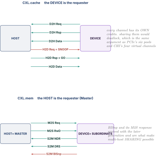
CXL.cache is defined as three message classes in each direction, six channels total, each with its own independent flow-control credits.
| Direction | Channel | What it carries |
|---|---|---|
| Device to host, D2H | Req | the device asking for a line, or evicting one |
| Rsp | the device answering a snoop | |
| Data | 64 bytes travelling upward | |
| Host to device, H2D | Req | snoops, the host telling the device to give a line up |
| Rsp | the host granting permission, the "global observation" message | |
| Data | 64 bytes travelling downward |
Two observations that carry most of the understanding.
H2D Req is snoops and only snoops. The host never asks a device for a line the way a device asks the host. The host's only request-direction message is "invalidate or downgrade what you hold." That asymmetry is Part 4.5 and it is the single most important structural fact about CXL coherence.
Six independent credit pools, not one. This is the deadlock argument from Part 4 of Interconnect and AMBA arriving off chip, and it is exactly the same argument, so recognise it rather than relearn it. If snoops and requests shared a credit pool, a device whose request queue is full and cannot drain because it is waiting for a response could block the very snoop whose completion would let it drain. That is a protocol-level dependency cycle, it deadlocks with no error indication, and the only structural fix is independent channels with independent credits. PCIe reached the same conclusion with its six separate credit pools for posted, non-posted, and completion traffic. CHI reached it with REQ, RSP, SNP, and DAT on separate virtual channels. CXL reaches it here. Three protocols, three eras, one argument.
4.3 A transaction walked end to end
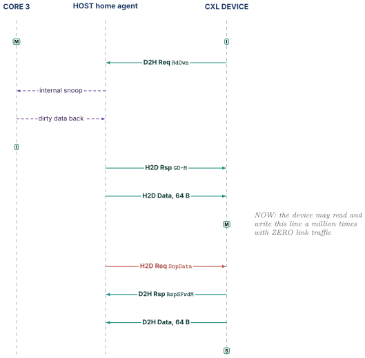
Concrete before abstract. The device wants to write a counter at host physical address , and the CPU currently holds that line dirty in its own cache. Walk every message.
1. The device misses in its own cache and issues a D2H Req. The opcode is RdOwn, which means "give me this line in a state where I may write it." The device also has RdShared for read-only access, and further opcodes for cases like reading a snapshot without keeping it. The request carries the address and a transaction identifier so the response can be matched back, exactly the AXI-ID role from Part 6.4 of Interconnect and AMBA.
2. The host's home agent resolves coherence internally. It consults its directory or snoop filter, sees that core 3 holds modified, and snoops core 3 over the on-chip fabric. Every mechanism in Cache Coherence Protocols executes here and none of it is visible on the CXL link. The device asked one question and the host did whatever its internal protocol requires to answer it. That encapsulation is the design, not an accident.
3. The host sends an H2D Rsp carrying a global-observation message. The family is written GO and it carries the state being granted, GO-M for modified, GO-E for exclusive, GO-S for shared, GO-I for none. Here it is GO-M. You own it, it is dirty, do as you like. The word "global observation" is worth unpacking because it is the semantic content. It is the host telling the device the rest of the system now agrees you have this permission, which is the moment the device's access becomes ordered with respect to everybody else's.
4. The host sends an H2D Data with the 64 bytes. Response and data are separate channels and can arrive in either order relative to each other, which means the device's transaction tracker must handle both orderings. That is a real piece of state-machine work and it is exactly the kind of thing formal verification is good at, which Part 11 returns to.
5. The device writes the line in its own cache and holds it in M. No further traffic. It may now increment that counter a million times at its own clock with the link completely idle.
6. Later, core 5 reads . The host's directory says the CXL device holds it. The host sends an H2D Req, a snoop. It is SnpData if a shared copy will do and SnpInv if the requester needs exclusivity.
7. The device answers on D2H Rsp and D2H Data. The response opcodes encode both the outcome and the resulting state, with names of the shape RspSFwdM, meaning "I have gone to Shared, and I am Forwarding you the data I held Modified." The 64 bytes ride the D2H Data channel.
8. The host supplies core 5 and updates its directory. Done.
4.4 Eviction, and the neat trick in the response
When the device wants to drop a line it holds, it does not simply push the data upward. It issues a D2H Req and waits. The opcode is CleanEvict if the line is unmodified and DirtyEvict if it is not.
The host responds with something in the GO_WritePull family, which means "acknowledged, and now send me the data." The device then puts the 64 bytes on D2H Data.
Why the extra round trip rather than just shipping the bytes? Because the host controls when it is ready to receive them, and folding that into the response makes the flow control implicit rather than requiring a separate credit scheme for evicted data. There is also a variant that tells the device to drop the data entirely, for cases where the host has determined the write-back is unnecessary. The host may already have the line, or the address may have been invalidated in between.
That is a small design idea and it is exactly the sort of thing worth noticing out loud in an interview. A response that carries a flow-control decision is cheaper than a response plus a credit.
4.5 The asymmetry, and why it is an interoperability decision
Here is the fact that separates candidates who have read a diagram from candidates who understand the protocol.
The coherence in Cache Coherence Protocols is symmetric. Every cache runs the same state machine. Every cache can be snooped by its peers. Every cache can answer a snoop with data. The protocol is a peer-to-peer agreement among equals.
CXL.cache is deliberately asymmetric. The host is the sole coherence authority. It owns the directory. It issues every snoop. It grants every permission. The device runs a reduced protocol. It may request, it may answer snoops, and it may evict. The device never snoops the host and never snoops another device. There is no message in the base protocol for it to do so.
Now the question an interviewer will ask, and the answer that separates you: why give up the symmetry?
The tempting answer is performance, and it is wrong. The right answer is interoperability.
A symmetric protocol requires both ends to implement the same coherence state machine, including its transient states, its race resolution, and its ordering guarantees. Those are the hardest and most vendor-specific parts of any processor design, they are frequently the subject of patents, and they differ substantially between one company's fabric and another's. Requiring a memory vendor's expander controller to implement a processor vendor's full coherence protocol would mean either publishing that protocol or restricting the ecosystem to one company. Both were unacceptable.
The asymmetric split is what avoids it. The host keeps its own internal protocol (MESI, MOESI, MESIF, whatever it happens to be, with whatever transient states and races it has) entirely private, and exposes a small, stable, publishable interface at the boundary. A device implements the small interface. It never needs to know what protocol the host runs internally, and the host never needs to disclose it.
Say exactly that in an interview and follow it with the consequence, which is the part that shows you have thought past the slogan: the price of the asymmetry is that everything routes through the host, so a device-to-device transfer that could physically go directly between two cards instead takes two hops through the root complex, and that is the cost the later peer-to-peer work in the standard is trying to claw back.
4.6 What implementing CXL.cache actually costs a device
Worth knowing because it explains why not every device wants it.
The device needs a real cache with real coherence states, at minimum M, E, S, and I, plus the transient states that cover the window between issuing a request and receiving both its response and its data. Part 7.1 of Cache Coherence Protocols describes exactly why transient states are where the bugs live, and nothing about that changes here except that the round trip is now hundreds of nanoseconds instead of tens, so there are far more transactions in flight and therefore far more transient state to track.
It needs an inbound snoop port that is always serviceable. This is the ACE lesson from Part 6.6 of Interconnect and AMBA restated. A device that can be snooped is no longer purely a requester, and it must be able to answer a snoop while its own requests are outstanding. If answering a snoop can be blocked by the device's own pending request, you have built a deadlock and it will find you under exactly the traffic pattern nobody tested.
It needs race handling for the case where a snoop and its own request cross on the wire. The device asks for a line. The host, before seeing that request, snoops the device for the same line. Both messages are in flight simultaneously in opposite directions. The protocol has rules for resolving that, and implementing them correctly is the single hardest part of a CXL.cache device.
None of that is cheap, and it is why Type 3 memory expanders (Part 6) do not implement CXL.cache at all. A memory expander never caches anything, so it needs none of this, which is precisely why memory expanders shipped first and in volume while coherent accelerators took longer.
05.Part 5, CXL.mem, the host reaching into device memory
5.1 Host-managed device memory, and the abstraction that matters
CXL.mem inverts the roles. Here the host is the master and the device is the subordinate, and the traffic is the host performing cache-line reads and writes against memory that physically lives on the device.
The memory involved is called host-managed device memory, universally abbreviated HDM. Three words, each load-bearing.
Host-managed means the host owns the address range, decides how it is mapped, and controls coherence over it. It is not a private device buffer that software reaches through a window.
Device means the physical media is on the far side of the link.
Memory means it appears in the host physical address map and is reached by ordinary loads and stores, not by a driver interface.
Now the abstraction that is easy to miss and is the best single insight in this part. The request that crosses the CXL link is not a DRAM command. It carries an address and asks for or supplies 64 bytes. It says nothing about rows, banks, columns, refresh, or timing. Everything in DRAM Controllers JEDEC and DFI happens on the device, behind the interface, where the host cannot see it and does not care.
The consequence is large. Because the interface is cache-line reads and writes rather than JEDEC commands, the media behind a CXL memory device does not have to be DDR at all. It can be DDR5, LPDDR, a stack of high-bandwidth memory, persistent memory, or something flash-backed with a DRAM cache in front. It can be a different generation of DDR than the host's own controller supports. A host built around DDR5 can have DDR4 hanging off a CXL port, which is a genuinely useful thing when you are trying to reuse a warehouse full of DIMMs.
That media independence is arguably a bigger deal than the capacity, and it is a strong point to make in an interview because most candidates only mention capacity.
5.2 The four channels, and the two that arrived later
CXL.mem's channels are named for the master-subordinate relationship.
| Direction | Channel | What it carries |
|---|---|---|
| Master to subordinate, M2S | Req | a request with no data: a read, an invalidate |
| RwD | request with data: a write, carrying the 64 bytes | |
| Subordinate to master, S2M | NDR | no-data response: a completion, an acknowledgement |
| DRS | data response: the 64 bytes coming back |
Notice the economy. A read is a request with no data and a response with data. A write is a request with data and a response with none. Splitting request-with-data from request-without-data into separate channels means a stream of small reads never queues behind a large write's payload, which is the same header-versus-data separation argument PCIe makes with its six credit pools in Part 8.2 of SoC Integration and Interfaces. Third time that argument has appeared in these notes. Notice it.
Two further channels came with the later generation of the standard and exist to let the device initiate coherence action: a back-invalidate snoop, written BISnp, and its response, written BIRsp. Get the directions from the meaning rather than memorising them. A back-invalidate snoop is the device telling the host to give a line up, so it travels upward, which on this protocol's naming is S2M BISnp. The host's answer travels back down, so it is M2S BIRsp. That is what the specification says, and deriving it from "who is talking to whom" rather than recalling a table is what stops you inverting it under pressure. Section 5.5 explains what the channel is for and why it changes what CXL can do.
5.3 A read walked, cycle by conceptual cycle
A core executes ld x1, [0x1_8000_0000] and that address falls in a CXL HDM window.
1. The load misses every level of cache. Ordinary business, all of Cache Organization and Prefetching.
2. The request reaches the host's home agent, which resolves coherence among the host's own caches first. If another core has the line, that is settled internally before anything crosses the link. This step happens identically whether the memory is a DIMM or a CXL device. That is worth stating because it is the reason CXL memory needs no new coherence model on the host side.
3. The home agent decodes the address to a CXL port using the HDM decoders programmed at boot in Part 3.2, and sends an M2S Req with the read opcode, the address, and a tag.
4. The request carries a small metadata field telling the device what coherence state the host is taking. This is how a device that keeps its own directory learns what the host holds. The public material describes this as a metadata field of a couple of bits with a selector. Treat the exact width as specification detail to confirm rather than quote.
5. The device's controller decodes and issues a media access. If the media is DDR5, this is where the entire content of DRAM Controllers JEDEC and DFI executes. The address mapping into bank, row and column. The row-buffer hit, miss or conflict. The JEDEC timers. The scheduler. A CXL memory expander contains a full DRAM controller and all of that note applies inside it. That is a genuinely useful thing to notice. The two notes compose rather than compete.
6. The device returns an S2M DRS carrying MemData with the 64 bytes and the matching tag. Depending on the flow it may also send an S2M NDR completion.
7. The host fills the cache and completes the load.
The whole thing is a request-response transaction with a tag, out-of-order completion, and credit-based flow control. If you have built an AXI master with outstanding transactions and IDs, from Part 6.4 of Interconnect and AMBA, you have built the shape of this. Say that.
5.4 A write, and why it still needs a completion
A write is an M2S RwD carrying the address and 64 bytes, answered by an S2M NDR completion.
Somebody always asks why a write needs a response when nobody is waiting for it. Three reasons and all three are real.
Resource reclamation. The host allocated a tracker entry when it issued the write. Without a completion it never knows when to free it, so the number of writes in flight would be unbounded, which means the tracker would have to be unbounded, which is not a design.
Ordering and fences. A memory barrier, or a persistence flush on a device with non-volatile media, has to know that a previous write reached a point of no return. That requires an acknowledgement from the device, not from the link.
Error reporting. A write can fail. The media can be bad, the address can be outside the configured range, or the device can be in an error state. Without a completion path there is nowhere for that to be reported, and a silently dropped write is the worst failure mode in computing.
Also note the partial write case, because it is the point where this note and DRAM Controllers JEDEC and DFI collide productively. A masked or partial write over CXL.mem, when the device protects its media with an error-correcting code, forces the device into a read-modify-write, because the check bits are computed over a whole granule and a partial write does not supply the whole granule. That is exactly the argument in Part 11.4 of the DRAM note and the mitigation is exactly the same. Coalesce partial writes until they form a full granule, or push back on whoever is generating them.
5.5 Who keeps the directory, and what back-invalidate changed
This is the part where the different flavours of HDM matter, and it is worth getting right because it is the natural follow-up to the bias question in Part 7.
For a plain memory expander, the situation is simple. Only the host caches that memory. The device never caches it, no other host has it mapped, so the host's own directory is a complete record of who holds what. Nothing on the device needs to track coherence at all. Public material labels this host-only-coherent HDM, usually written HDM-H.
For an accelerator that both exposes memory to the host and wants to use that memory itself, the situation is not simple, because two agents now cache the same lines. Something has to arbitrate. The original mechanism handled this through the bias model of Part 7, which borrows CXL.cache messages to do the coordination. That flavour is usually written HDM-D.
The later generation added a third path, and it is the interesting one. Give the device its own snoop filter or directory, and give it a channel on which to act, the BISnp back-invalidate snoop. Now the device can, on its own initiative, tell a host to invalidate a line it holds. The flavour is usually written HDM-DB, the B for back-invalidate.
Notice why that is a bigger change than it looks. With back-invalidate, a memory device becomes an agent that can initiate coherence rather than only respond to it. That is the enabling mechanism for genuine multi-host memory sharing in Part 8.4, because sharing requires that when host A takes a line for writing, hosts B and C are told to drop their copies, and the only party that knows all three hold it is the device.
The storage cost is the snoop-filter arithmetic from Part 5.3 of Cache Coherence Protocols, applied to a much larger memory. Work an illustration. A 256 GB device with 64-byte lines has billion lines. Even two bits of state per line is over a gigabyte of tracking metadata, which is why devices keep this in their own DRAM alongside the data rather than in SRAM, and why a directory lookup can itself cost a media access. That is a real and often-missed cost of device-side coherence, and mentioning it unprompted is a strong signal. The standard mitigation is the same one from the coherence note. Track coarser than a line, accept imprecision, and send some unnecessary invalidations.
Hedge this properly if pushed. The mapping of these flavours onto specific specification revisions is exactly the kind of detail that is easy to get subtly wrong, and a confident wrong version number costs more credibility than a hedge. The right thing to say is that the capability exists, describe what it does, and say you would check the revision.
06.Part 6, the three device types
6.1 The types fall out of the protocols, they were not invented separately
Do not memorise the three types. Derive them, because then you can never get them the wrong way round, and getting them the wrong way round is the most common self-inflicted wound in a CXL interview.
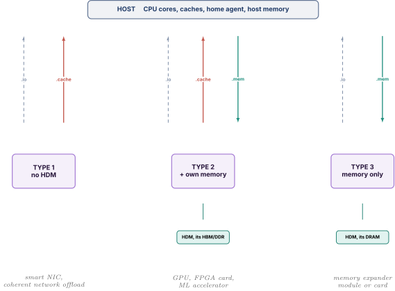
CXL.io is mandatory, so every device has it. That leaves two optional protocols and therefore four combinations. One of them, the combination with neither optional protocol, is just a PCIe device. The remaining three are the device types.
| CXL.io | CXL.cache | CXL.mem | What that combination means | |
|---|---|---|---|---|
| Type 1 | yes | yes | no | the device caches host memory, and has no memory of its own to expose |
| Type 2 | yes | yes | yes | traffic in both directions: the device caches host memory and the host reaches device memory |
| Type 3 | yes | no | yes | the host reaches device memory, and the device caches nothing |
Read the middle two columns as directions rather than features and it becomes obvious. CXL.cache is the device reaching up. CXL.mem is the host reaching down. Type 1 reaches up only. Type 3 is reached down into only. Type 2 does both.
6.2 Type 1, the coherent device with no memory to give
Protocols. CXL.io plus CXL.cache. No HDM at all.
What it is for. A device that needs to participate in host coherence but has nothing to contribute to the address map. The canonical example is a network interface or a network-offload engine that maintains queues, doorbells, and completion structures in host memory and wants to touch them coherently and atomically rather than through the DMA-plus-flush dance of Part 1.3.
Why the case is real, worked. A high-rate network device processing small packets must update a receive queue's producer index on every packet. At ten million packets per second, that is ten million updates to a small number of hot cache lines that the host's software is simultaneously reading. Without coherence, each update is a DMA write plus whatever cache maintenance the driver has to perform on the read side, and the two sides interfere. With CXL.cache, the device holds the line, performs an atomic update, and the host's read triggers exactly one snoop.
The honest caveat. Type 1 is the type with the fewest publicly identifiable shipping products, and the reason is Part 4.6. Implementing a coherent cache with transient states and snoop servicing is expensive, and for a lot of devices the DMA path is good enough. Say that plainly if asked. Naming a category is safer than naming a product you are not certain ships.
6.3 Type 2, the accelerator with its own memory
Protocols. All three.
What it is for. An accelerator that has substantial local memory (high-bandwidth memory on package, or a bank of DDR on the card) and wants two things at once. It wants to reach into host memory coherently, because the data structures it operates on live there. And it wants the host to be able to reach into its memory, because the host needs to fill inputs and collect results without a bulk copy.
Why both directions matter, concretely. Take a graph-analytics accelerator. The graph's edge list is 200 GB and lives in host memory. The accelerator streams and randomly probes it, which is exactly the case Part 1.3 showed bulk copy handles badly. The accelerator's working state (frontier sets, partial results) is 32 GB and lives in its own high-bandwidth memory, which it hammers at terabytes per second. The host wants to read the results as they emerge without stopping the kernel.
That is CXL.cache reaching up for the edge list and CXL.mem reaching down for the results, simultaneously, on the same link.
And that is exactly why Type 2 is the only type that needs a bias model. Two agents now have legitimate claims on the same physical memory. The device owns it locally, and the host has it mapped. Part 7 is entirely about resolving that.
Examples. The category is accelerators with attached memory, meaning programmable-logic cards, machine-learning engines, and graphics processors, with several vendors having publicly announced CXL support in these categories. Product-level specifics move quickly enough that the right posture in an interview is to describe the category and, if pressed for a name, say which company you believe has announced something and flag that you would check the current status.
6.4 Type 3, the memory expander, and why it shipped first
Protocols. CXL.io plus CXL.mem. No CXL.cache.
What it is. Memory, behind a controller, behind a CXL link. The device caches nothing. It answers reads and writes. That is the whole function.
Why it is the simplest device to build, and this is worth spelling out because it explains the market. Look back at Part 4.6's list of what CXL.cache costs a device. A coherent cache, transient states, an always-serviceable snoop port, race resolution between crossing messages. A Type 3 device needs none of it. It has no cache, so it has no coherence states, so it has no transient states, so it has no races. It is a request-response slave with a memory controller behind it. All of the genuinely hard protocol work disappears.
What is left is work the industry already knows how to do: a link layer, a decoder, a DRAM controller from DRAM Controllers JEDEC and DFI, an error-correcting-code path, and a set of management registers. That is why memory expanders were the first CXL products to reach volume, and it is a good answer to "why has CXL adoption been uneven across the device types."
Examples. Memory-expansion modules and add-in cards from the major DRAM vendors, plus a set of merchant controller chips from companies whose product is the CXL-to-DRAM controller itself rather than the module. Public announcements in this category include modules in the roughly 96 GB to 256 GB range using CXL 2.0-class controllers, and controller silicon sold to module makers. Capacities and generations move, so quote the shape and not the specification.
One nuance worth having ready. Because a Type 3 device presents a memory range and nothing else, and because that range appears as a CPU-less NUMA node, a Type 3 device is almost entirely a software-visible object with no software work required. No driver is in the data path. That combination of enormous system impact and near-zero device complexity is unusual and is most of why the category caught on.
07.Part 7, the bias model, which is the question you will be asked
7.1 The collision that creates the problem
Type 2 only. A Type 1 device has no memory to bias and a Type 3 device has no local compute to bias it for.
Set up the collision concretely. An accelerator has 16 GB of high-bandwidth memory. That memory is exposed as HDM, so the host has it in its address map and may load and store to it coherently. The accelerator also uses that memory as its own working store, at whatever rate its local port sustains. For an on-package high-bandwidth stack that is in the region of several hundred gigabytes to a couple of terabytes per second, depending on generation.
Now ask the naive question. If the host might have any of those lines cached, does the accelerator have to check with the host before every local access?
Count what "yes" costs. Take the accelerator's local memory bandwidth as 800 GB/s, which is a reasonable order of magnitude for a single modern high-bandwidth stack. In 64-byte lines that is
Every one of those would become a CXL transaction. The link carries 63 GB/s each way. Even ignoring headers entirely and counting only the data, the link would need
which is thirteen times more than the link can carry. And each access would take a link round trip (hundreds of nanoseconds from Part 9) instead of the tens of nanoseconds a local access takes.
So the naive answer destroys the machine. You attached high-bandwidth memory to an accelerator specifically so it could be accessed fast and locally, and then you routed every access through a link an order of magnitude narrower and an order of magnitude slower. You have built a very expensive way to be slow.
The bias model exists to make the common case not do that.
7.2 The two states, stated plainly
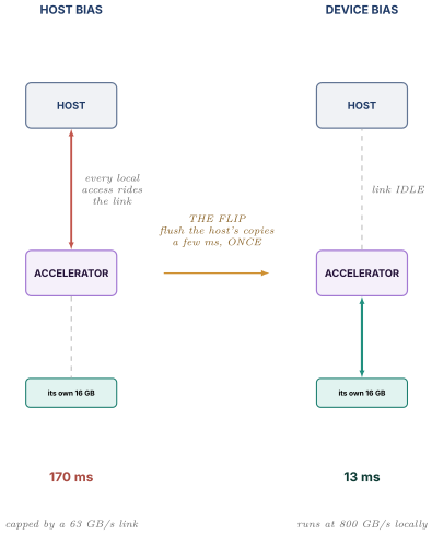
Host bias. The device's memory behaves like ordinary host memory. The host may cache it freely. When the device wants to access it, the device goes through the host. It sends a request up, the host resolves coherence, and the answer comes back. Correct, safe, and slow for the device. Fast and unremarkable for the host.
Device bias. The device is guaranteed the host does not hold those lines cached. The device therefore accesses its own memory directly, with no CXL traffic whatsoever. Fast for the device.
The two sentences to be precise about, because both are where people go wrong:
Bias is not a permission scheme. It does not say who is allowed to access the memory. In both states, both parties may access it, and coherence is preserved in both states. What bias changes is the path an access takes and therefore what it costs.
Bias is a property of a region of memory, not of the device. Different regions can be in different states at the same time. Public descriptions of the mechanism generally present it at page granularity with the device keeping a bias table, so a device might have one buffer in device bias while another is in host bias.
7.3 The scenario, worked, which is the answer to the interview question
This is the example to rehearse. It is small enough to do on a whiteboard in ninety seconds and it produces a number.
The setup. An accelerator runs a kernel that makes ten passes over a 1 GB input buffer held in its own memory. Accesses are 64 bytes.
Under host bias. Every access is a CXL round trip. The data alone is
crossing a 63 GB/s link, so at best
and that is the optimistic figure, ignoring request headers, ignoring that the accelerator needs enough outstanding transactions to fill a link with a several-hundred-nanosecond round trip, and ignoring that the link is now unavailable for anything else for the whole 170 ms.
Under device bias. Zero CXL traffic. The accesses go to local memory at 800 GB/s.
and the factor is not a coincidence, it is exactly the ratio of local memory bandwidth to link bandwidth, which is the honest way to state the whole benefit. Device bias is worth the ratio of the device's local bandwidth to its link bandwidth, and nothing more. On a device whose local memory is no faster than its link, bias buys you latency and not much else.
Now the flip cost, which is the half nobody works. Moving that 1 GB from host bias to device bias means guaranteeing the host holds none of it. If the host wrote the whole buffer while filling it, its last-level cache holds at most its own capacity of the buffer (say 256 MB, so 4 million lines), and every one has to be written back and invalidated. Even at a generous few nanoseconds per line amortised, that is a one-time cost in the low milliseconds, plus the page-table and bias-table bookkeeping.
Put the two together and the entire engineering content of the bias model falls out in one line.
Bias is a mode with a switching cost, so it pays exactly when the phase is long relative to the flip.
Amortised over ten passes, a few milliseconds of flip against 157 ms saved is obviously right. Amortised over one 64-byte access, it is catastrophic. A device that flips bias per access has built a machine that does nothing but flip bias.
And notice what shape that argument is. It is the break-even between a fixed switching cost and a per-unit running saving, which is exactly the inrush-current and break-even-idle-time argument in Part 6.3 of Power Fundamentals and Clock Gating, and exactly the open-page-versus-closed-page break-even in Part 6.3 of DRAM Controllers JEDEC and DFI. Three different domains, one piece of reasoning. Saying that out loud is worth more than the number, because it shows the reasoning is yours.
7.4 How the flip actually happens, hedged where it should be
Two paths are described in the public material and it is worth knowing both exist while being careful about the details.
Software-assisted. Software, typically the accelerator's driver or runtime, decides that a region is about to become device-private and requests the transition. The host flushes and invalidates its copies of the affected lines. The device updates its bias table for those pages. Afterwards the device may access them without asking. The reverse transition gives the region back. This is the path most commonly described in introductory material, at page granularity, and it fits the phase-based usage model naturally. A runtime that knows it is about to launch a kernel over a buffer knows exactly when to flip.
Hardware-autonomous. The device detects, on its own, that it is repeatedly having to go through the host for a region and initiates the transition itself, without software involvement. The attraction is obvious, since software does not always know the access pattern, and so is the risk, which is that an autonomous mechanism with a switching cost can oscillate if the workload alternates. Any implementation needs hysteresis for exactly the reason an adaptive page policy in a DRAM controller does.
Be careful here. The precise division of responsibility between the specification, the host, the device, and the driver in the bias-flip flow is a place where introductory summaries disagree with each other, and it is the sort of thing to describe by mechanism and hedge on detail. A good interview answer says what the two states are, why they exist, what the flip costs, and that the transition is coordinated between device and host with both software-directed and device-initiated paths described, and then offers to look up the exact message sequence.
7.5 Why back-invalidate changes the framing
Part 5.5 introduced the back-invalidate channel. Notice what it does to this part.
The bias model, in its original form, is a mechanism for a device to avoid asking permission by arranging in advance that permission is not needed. It is a coarse-grained, phase-oriented answer, and its coarseness is the source of both its benefit and its awkwardness.
Back-invalidate gives the device a different tool, the ability to reclaim a line from the host on demand, at line granularity, at the moment it needs it. A device with its own directory and a BISnp channel does not have to arrange anything in advance. It looks up its directory, sees the host holds the line, snoops it back, and proceeds.
That is a fine-grained answer to the same problem, and the honest framing for an interview is that the two coexist rather than one replacing the other. Coarse-grained bias remains the right tool when a whole buffer is about to be worked on privately for a long phase, because it eliminates per-line tracking entirely. Fine-grained back-invalidation is the right tool when access is genuinely interleaved and no phase structure exists to exploit. Saying that the newer mechanism does not obsolete the older one, and explaining when each wins, is a much stronger answer than declaring a winner.
08.Part 8, pooling, sharing, and the fabric
8.1 Stranded memory, counted
Start with the economics, because this part is the only one in the note whose motivation is not a hardware constraint.
Twenty servers in a rack. Each has 512 GB installed. Each was sized for its own peak, because a server that runs out of memory does not degrade, it fails. But peaks do not coincide. At any moment some servers are at 90 percent and others at 20 percent, and the average across the rack sits far below the provisioned total.
The gap is stranded, meaning installed, paid for, powered, and unusable by anybody except the one server it is bolted to. Published analyses from cloud operators have put the stranded fraction of fleet DRAM in a range with figures around a quarter appearing in the literature. Treat that as an order of magnitude from public studies rather than a precise constant, since it depends entirely on the fleet and the scheduling policy.
Now the alternative. Give each server 320 GB locally and put 2 TB in a shared pool the rack can draw from.
An 18 percent reduction in installed DRAM. More importantly than the percentage, any single server can now reach far above its local 320 GB when it needs to, which the old arrangement could not do at any price short of rebuilding the machine.
The mechanism is statistical multiplexing and it is the same argument as an airline overbooking, a shared thermal budget across cores, or a shared power budget across a rack. It works exactly to the extent that the peaks are uncorrelated, and it fails badly when they are not, which is the honest caveat and the right thing to volunteer before an interviewer raises it.
8.2 Switching, and the multi-logical device
Getting from "one host, one device" to "many hosts, a pool" requires two things.
A switch. CXL switches sit between host ports and device ports and route transactions, in the same structural role as a PCIe switch and reusing the same physical layer. A switch means a host port can reach many devices and a device port can be reached by many hosts.
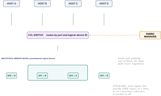
A way for one physical device to be divided among hosts. This is the multi-logical device, MLD. A single physical memory device presents itself as several independent logical devices, each with its own identifier, its own capacity, and its own assignment. Published material for the switching generation of the standard describes up to sixteen logical devices per physical device. A device that presents just one is a single logical device, SLD.
The identifier, the LD-ID, travels with transactions so the device can tell whose request it is servicing and enforce isolation between them. That is the same idea as a requester ID on PCIe or a source identifier on a network-on-chip, and it does the same three jobs: routing the response back, enforcing isolation, and attributing bandwidth for quality of service.
A fabric manager is the entity that decides the assignment: which logical device belongs to which host, when capacity is added or removed, and what happens on a hot-plug event. It is defined as a management entity with an interface rather than as a piece of hardware, and it can be implemented in a baseboard management controller, in the switch's own firmware, or in a rack-level orchestration service. The practical point for a hardware engineer is that binding and unbinding are management-plane operations happening out of band, not something the data path negotiates.
8.3 Pooling against sharing, which is a trap question
These two words are used loosely in trade press and precisely in the standard, and an interviewer who uses them precisely is testing whether you do.
Pooling. A region of the pool is assigned to exactly one host at a time. Reassignment is a management operation. Unbind from host A, and then it can be bound to host B. From the hardware's point of view there is no coherence problem at all, because there is never more than one cacher. Pooling is a capacity-allocation feature.
Sharing. Two or more hosts have the same region mapped simultaneously, and both may cache lines from it, and the hardware keeps them coherent. Now there is a genuine multi-host coherence problem. When host A takes a line for writing, hosts B and C must be made to drop their copies.
What sharing needs that pooling does not is exactly the mechanism from Part 5.5. The device must keep track of which hosts hold which lines, and it must be able to act on that knowledge by initiating an invalidation. That is a device-side directory plus the back-invalidate channel. Neither is required for pooling.
The trap. Calling pooling "shared memory." It is not. Pooling is time-shared capacity with a single owner at any instant. Sharing is simultaneous coherent access by multiple hosts. Getting this distinction right, unprompted, is one of the cheapest strong signals available on this topic, and getting it wrong tells an interviewer you learned CXL from a marketing deck.
A second trap is worth naming. Even with hardware coherence across hosts, sharing does not give you a distributed programming model for free. Two hosts running two operating systems with two separate page tables both mapping the same physical region still need to agree on what the data structures in it mean, who allocates, and what the failure semantics are when one host dies mid-update. Hardware coherence solves the visibility problem and leaves the agreement problem entirely to software. Saying that shows you have thought about the system and not just the wire.
8.4 The fabric direction, described as capability rather than version
The standard has moved steadily from "a link" toward "a fabric," and the specific capabilities are worth knowing while the version mapping is worth hedging.
Multi-level switching. Early switching support was a single switch level between hosts and devices. Later revisions allow switches to connect to switches, which is what turns a star into a network and lets a pool span more than one enclosure.
Port-based routing. Rather than routing purely by the tree structure PCIe inherited, transactions carry a destination identifier and are routed by it. Published material describes support for up to 4096 nodes in the fabric, with transactions carrying a destination identifier and, where needed, a source identifier. The practical consequence is that inter-switch links can carry traffic belonging to many different host-device relationships at once, which a strict tree cannot express.
Global fabric-attached memory. A memory device that is not bound beneath any one host's hierarchy but sits in the fabric as a shared resource, configured by one owner or by the fabric manager and then reachable by many hosts and devices. This is the structure that makes rack-scale disaggregated memory a thing you could build rather than a thing you could describe.
Peer-to-peer between devices. Part 4.5 noted that the base coherence model routes everything through the host, which means two accelerators on the same switch exchange data by two hops through the root complex. Later work in the standard addresses direct device-to-device paths. The details are exactly the sort of thing to look up.
How to talk about versions. The consortium has shipped a succession of revisions. A 2.0 generation brought switching and pooling. A 3.0 generation brought the 64 GT/s data rate, the 256-byte flit, back-invalidation and the fabric. Further 3.x revisions added fabric-management APIs, security, and manageability. A 4.0 specification released at the end of 2025 moves the link to PCIe 7.0's 128 GT/s while keeping the 256-byte flit. The 4.0 addition worth knowing by name is port bundling, which lets a host and a Type 1 or Type 2 device aggregate several physical ports into one logical attachment, so aggregate bandwidth to a single device can grow by adding ports rather than by waiting for the next PCIe generation. It also adds a native x2 link width and support for deeper retimer chains, which is a reach-and-topology change rather than a protocol one. Describe capabilities and hedge the mapping. "Switching and pooling came in around the 2.0 generation, back-invalidate and the fabric work came with 3.0, and 4.0 is the move to the 128 GT/s PCIe generation plus port bundling, but I would check the exact revision" is a completely acceptable and honest sentence. Asserting a wrong version number confidently is not, and it is the single easiest way to lose credibility on this topic, because the person asking almost certainly has the specification open in another window.
09.Part 9, latency, told honestly
9.1 Where the nanoseconds go, built up term by term
Every enthusiastic description of CXL eventually meets this section, and the candidates who handle it well are the ones who volunteer it rather than being cornered into it.
CXL-attached memory is slower than local DRAM. It is not close. It cannot be made close. Build the budget and see why.
Start from the reference point in Part 3.2 of DRAM Controllers JEDEC and DFI. Idle memory latency measured from a core on a modern local-DIMM system lands broadly in the 60 to 90 nanosecond range, of which the DRAM device itself is well under half and the rest is fabric, controller queueing, and the fill path.
A CXL read pays all of that, on the device side, and then adds:
| Term | Rough contribution | Can you attack it? |
|---|---|---|
| host fabric to the CXL port | tens of ns | floorplan, same as any fabric |
| host CXL controller and link layer | tens of ns | yes, this is design |
| SerDes out and back, pin to logic | roughly 20 to 25 ns round trip | no |
| a retimer, if the channel needs one | on the order of 10 ns each | avoid it, or shorten the channel |
| a switch, if present | another store-and-forward hop | avoid it for latency-critical memory |
| device link layer and controller | tens of ns | yes, this is design |
| the device's own DRAM access | the whole of the DRAM note | yes, scheduling and address map |
| return path | repeat the link terms | no |
Treat every one of those as an order of magnitude rather than a specification. The SerDes figure in particular comes from published controller-vendor material and varies with whether the two ends share a reference clock.
What the standard asks for. Widely quoted figures from the consortium's own material state target pin-to-pin latencies of under 50 nanoseconds for a snoop response and under 80 nanoseconds for a memory read. Note carefully what "pin to pin" excludes. It is the device's contribution measured at its own package boundary, not what a core sees. Quoting it as though it were the end-to-end number is a common and detectable mistake.
What is actually measured. Public figures disagree with each other by a lot, and the honest thing is to say so. Controller vendors have published adders in the region of tens of nanoseconds per direction. Early module measurements have been reported at figures such as around 130 nanoseconds of added latency, with expectations of improvement. Academic measurement work has reported CXL memory access latency at roughly 2.2 times an eight-channel local DDR5 configuration. Other summaries put typical controller-added latency at 100 to 200 nanoseconds, and some measurements of complete modules run considerably higher.
The defensible summary, and the one to say in a room: first-generation CXL-attached memory lands somewhere in the region of two to three times local DRAM latency for a directly attached device, more behind a switch, and the spread across published measurements is wide enough that I would measure the specific part rather than quote a number.
That sentence is worth more than any of the individual figures, because it is both true and checkable.
9.2 The latency ladder, and the one comparison that matters
Put CXL on a ladder with everything else and one fact jumps out.
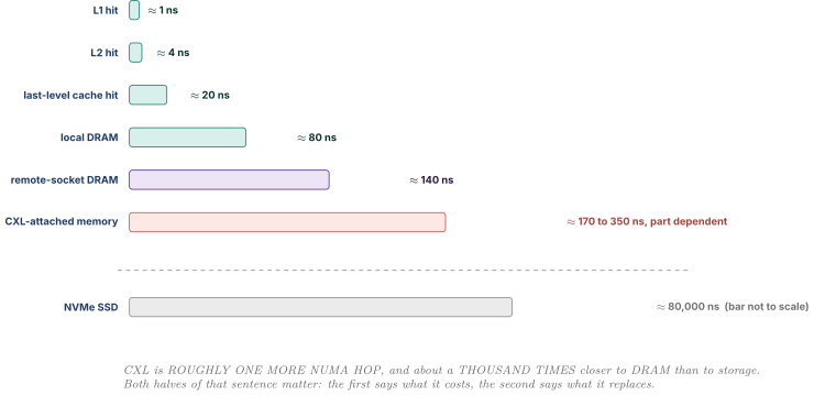
The observation to lead with: CXL memory sits next to a remote-socket NUMA access, not next to storage. That is why operating systems model it as a CPU-less NUMA node rather than inventing something new, and why every mechanism the kernel already had for NUMA (distance tables, allocation policy, migration, page reclaim) works on it from the first day.
9.3 Which workloads tolerate it, worked three ways
Do not answer "it depends." Do the arithmetic for three workloads and let the numbers answer.
Model a core at 3 GHz, so a cycle is 0.333 ns. Assume that without cache misses it retires 2 instructions per cycle.
Workload A, streaming with high memory-level parallelism. A large sequential scan. Misses are frequent but independent, so dozens are outstanding at once and their latencies overlap completely. Latency is irrelevant. Only bandwidth matters. That is the good news and it immediately becomes the bad news, because it means performance now tracks the one number CXL is worse at. One x16 Gen5 device carries 63 GB/s per direction. The eight local DDR5 channels of Part 1.1 carry 307 GB/s. Measured devices do worse than the link's headline figure. The MICRO 2023 characterisation of real CXL-ready parts found two local DDR5 channels delivering roughly 3.4 times a single CXL device's read bandwidth. Verdict: this workload does not care about the latency and cares enormously about where you put it. Move a bandwidth-bound scan wholesale onto one CXL device and it gets slower in proportion to the bandwidth ratio, which is the opposite of the usual claim about streaming workloads.
The real win for this workload is that CXL bandwidth is additive. Spread the scan across local DRAM and one or more CXL devices and the aggregate goes up, because the CXL link is a set of wires that were not carrying memory traffic before. That is the one workload class for which interleaving across the tiers is the right answer rather than the wrong one, which Part 9.6 comes back to.
Workload B, pointer chasing. A hash-table probe chain or a graph traversal where each load's address depends on the previous load's result. Memory-level parallelism is essentially one. Every miss is fully exposed. Say one dependent miss per 10 instructions.
Local DRAM. Ten instructions is 5 cycles of work plus cycles of stall.
CXL at 250 ns. cycles of stall.
Three times slower. Verdict: this workload cares enormously. Never put a pointer-chasing hot structure on CXL memory.
Workload C, a large in-memory dataset with a hot working set, and this is the one that matters. 500 GB of data. The hot working set that receives 95 percent of accesses is 20 GB. Put 128 GB in local DRAM and the rest on CXL.
An 11 percent average latency penalty in exchange for four times the memory. And if the fast-tier hit rate falls to 50 percent,
which is roughly double local DRAM. State the comparison as the penalty rather than the raw number and it is stark. The penalty went from 11 percent to 106 percent, so a hit rate that fell by half multiplied the penalty by ten. That non-linearity is the whole point. The average is dominated by the slow tier the moment the fast tier stops absorbing nearly everything. The entire question is the hit rate on the fast tier.
Now notice what that equation is. It is
which is exactly the average-memory-access-time equation from Cache Organization and Prefetching, with the local DRAM playing the role of the cache and the CXL memory playing the role of the backing store. That is not an analogy. It is the same equation, and tiering is a cache-management problem with pages as the block size. Say that in an interview and the rest of the tiering discussion writes itself, because every intuition about capacity, associativity, replacement policy, and working-set size transfers directly.
9.4 The comparison that actually justifies the technology
Workload C's 11 percent penalty looks like a cost. It is not. It is a saving, and framing it correctly is the difference between a defensive answer and a confident one.
The alternative to putting 380 GB on CXL was not putting it in local DRAM. If local DRAM could have held it, nobody would have bought a CXL device. The alternative was not having it in memory at all, which means those 5 percent of accesses go to storage.
CXL memory is not competing with local DRAM. It is competing with not having the memory. Against local DRAM it loses by a factor of three. Against storage it wins by a factor of forty-six. Which comparison is the right one is determined entirely by whether the data fits locally, and it usually does not, which is why the product exists.
That is the single most useful paragraph in this note for an interview. Rehearse it.
9.5 Tiering, and the break-even on a page migration
If tiering is a cache problem, the interesting engineering is the replacement and promotion policy, and here the block size (a 4 KiB page rather than a 64-byte line) changes everything.
Demotion. Cold pages move from the fast tier to CXL. The kernel already had this machinery. It used to move cold pages to swap, and a CXL node is simply a much better destination.
Promotion. Hot pages move back. The hard part is detecting which ones. The available signals are page-table access bits sampled periodically, deliberate access faults of the kind NUMA balancing uses, sampling-based access monitors, and hardware access counters where the platform provides them. All of them trade sampling overhead against detection accuracy and none is free.
Now the break-even, which is the number worth carrying. What does one page migration cost?
The copy itself is small, since 4 KiB at a few gigabytes per second effective is well under a microsecond. The expensive part is the translation-lookaside-buffer shootdown. Moving a page changes its physical address, so every core that might hold a translation for it must be told to discard it, which on a many-core machine is an inter-processor interrupt storm plus a synchronisation barrier. Published measurements of shootdown cost vary enormously with core count and kernel version, but the order of magnitude on a large machine is microseconds, not nanoseconds. Take 10 µs as an illustration and flag it as illustrative.
Each subsequent access to that page now saves ns. So the migration pays back after
A 4 KiB page holds 64 cache lines. So the page has to be touched roughly once per line before the migration breaks even. That is, read through about once. Any page hotter than that is worth promoting. Any page colder is not.
Two design conclusions fall straight out of that, and both are the kind of thing an interviewer is fishing for.
Promote on repeated hotness, never on first touch. A single access to a cold page is not evidence. It costs 59 accesses to be wrong. This is why promotion policies use multiple observations and hysteresis rather than reacting immediately, and it is the same reasoning as a branch predictor's two-bit counter refusing to flip on one mispredict.
Batch the shootdowns. Because the fixed cost is dominated by the shootdown rather than the copy, migrating 32 pages in one batch costs barely more than migrating one. That changes the policy from "promote this page" to "accumulate a promotion set and flush it periodically," which is the same amortisation argument as write draining in Part 6.4 of DRAM Controllers JEDEC and DFI. Pay one turnaround for many transfers rather than one per transfer.
And notice, again, the shape. A fixed switching cost, a per-unit running saving, a break-even. Bias flipping in Part 7.3. Power gating in Power Fundamentals and Clock Gating. Open page against closed page in the DRAM note. Four instances of one argument. An interviewer who hears you recognise the pattern rather than recompute it learns something real about how you think.
9.6 Interleaving, and a decision worth having an opinion about
The hardware can interleave addresses across CXL devices, and across CXL and local DRAM, in the same way a memory controller interleaves across channels.
Interleaving across several CXL devices is straightforward and usually right. It aggregates their bandwidth and spreads hot spots, exactly as channel interleaving does in DRAM Controllers JEDEC and DFI.
Interleaving local DRAM with CXL memory is a different and more interesting question, and it makes a good discussion point because there is a real argument on each side.
For. You get the sum of the bandwidths, automatically, with no software involvement, and no page ever needs migrating because every page is already spread across both tiers.
Against. You also get the average latency on every single access, permanently, with no way for software to opt out. The workload that would have kept its hot pointer-chasing structure entirely in local DRAM now finds half of it on the far side of a link. Hardware interleaving destroys the very locality that tiering exists to exploit.
Here is the defensible position, and the one to state. Interleave across devices within a tier, keep the tiers separate so that software can place data, and let the operating system's page placement do the tiering. Then add the honest caveat, that this depends on software actually doing the placement well, and that on a workload with no exploitable locality, hardware interleaving's guaranteed bandwidth may genuinely beat software tiering's failed attempt at locality. Workload A of Part 9.3 is exactly that case. A bandwidth-bound streaming scan has no locality for tiering to exploit and its whole benefit from CXL is the extra wires, so interleaving it across the tiers is right for precisely the reason interleaving Workload B would be wrong. Having a position and knowing its failure case is the answer. Having a position and defending it absolutely is not.
10.Part 10, how this compares to the coherence you already know
This part is where the interview goes, on the evidence of how the questions in Part 12 are shaped. The two notes it draws on are Cache Coherence Protocols and Interconnect and AMBA, and the value here is entirely in the mapping.
10.1 Against the multicore coherence of note 10
What is the same, and it is more than people expect. The states are MESI. The problem is the same problem. Multiple caches, one address, one coherent view. The two invariants from Part 1.4 of Cache Coherence Protocols (single writer or multiple readers, and data value propagation) hold unchanged. The transient states are transient states. The races are races. If you can reason about a MESI race you can reason about a CXL race, and you should say so.
What is different, in four points.
Symmetry. Note 10's protocols are peer-to-peer among equals. CXL.cache is host-authoritative. The host snoops, the device answers, and the device never snoops anybody. Part 4.5 argued that this is an interoperability decision rather than a performance one, and that is the framing to use.
Latency, by an order of magnitude. An on-chip snoop round trip is tens of nanoseconds. A CXL snoop round trip is hundreds. The consequence is not that things are slower, it is that far more transactions are in flight at once, so the tracker structures are deeper, the transient-state space is larger, and the race window is wider. A protocol that is easy to get right at 40 ns is materially harder at 400 ns for exactly this reason, and naming that consequence is a much better answer than "it's slower."
Where the point of coherency lives. On chip it is a home node or a shared last-level cache. Across CXL it is the host, always, in the base model, until back-invalidation gives a memory device a limited ability to initiate, which is a genuine change in the shape of the protocol and not just an added message.
Failure model. Two cores on one die do not become disconnected. A CXL device can be unplugged, can lose its link, can go into an error state, and can be hot-added. Coherence protocols designed for on-die use generally do not have a story for a participant vanishing. A link-based one must.
10.2 Against CHI, which is where the mapping is nearly exact
This is the most valuable single item in the note for an interview, because it converts material the reader already knows into material the interviewer is asking about.
From Part 6.7 of Interconnect and AMBA, CHI has request nodes, home nodes, and slave nodes, with four message classes on independent virtual channels. Lay CXL beside it.
| CHI | CXL | Both are |
|---|---|---|
| RN-F, a fully coherent request node with a cache | a Type 1 or Type 2 device | an agent that caches memory it does not own |
| HN-F, the home node: directory, snoop filter, point of coherency | the host | the sole coherence authority for an address range |
| SN-F, a slave node: memory, no coherence responsibility | a Type 3 device | a memory target that answers reads and writes |
| REQ, request node to home | D2H Req | "I want this line" |
| SNP, home to request node | H2D Req | "give this line up" |
| RSP | D2H Rsp / H2D Rsp | permissions and acknowledgements |
| DAT | D2H Data / H2D Data | 64 bytes |
| home node to slave node | CXL.mem, M2S / S2M | the coherence point talking to memory |
| four classes, four virtual channels | six or more channels, independent credits | the deadlock-avoidance argument of note 11 Part 4 |
Read the last two rows together and the whole architecture snaps into focus. Say it in one sentence:
CXL.cache is the off-chip version of the request-node-to-home-node link, and CXL.mem is the off-chip version of the home-node-to-slave-node link.
That sentence, delivered unprompted, tells an interviewer that you did not learn CXL as a list of acronyms. It is the highest-leverage thing in this note.
Where the mapping breaks, and say this too. CHI is symmetric among its request nodes and lives inside one coherent domain designed by one company. CXL is asymmetric by design and crosses a vendor boundary. CHI request nodes can be many and peer-like. CXL routes everything through the host in the base model. And CHI never has to worry about a node being physically removed.
10.3 Against a DRAM controller, which is a different kind of comparison
Worth one paragraph because it prevents a category error.
CXL.mem is not a competitor to the DDR interface. It sits above it. A Type 3 device receives a CXL.mem read and, inside itself, performs the entire content of DRAM Controllers JEDEC and DFI: address mapping to bank and row and column, row-buffer hit or miss or conflict, JEDEC timing legality, scheduling, refresh, and error correction. The two notes compose. A memory expander is a CXL front end bolted to a DRAM controller, and the DRAM controller inside it is exactly the block that note describes.
The one thing the CXL layer changes is what the DRAM controller sees. Requests arrive with more latency tolerance already baked in. The host has already paid a link crossing, so a few extra nanoseconds of scheduling to convert a conflict into a hit is a better trade than it would be for a local controller. That is a real and specific design consequence, and it is the kind of observation that lands well.
10.4 Against socket-to-socket links, where the misconception lives
A common and wrong claim is that CXL replaces the proprietary coherent links between processor sockets.
Those links (every major vendor has one) are symmetric, full-coherence links between peers running the same protocol from the same company, tuned aggressively for latency, and free to expose whatever internal protocol details they like because both ends are the same design. CXL is asymmetric, deliberately restricted, and built to cross a vendor boundary, and it pays a latency price for the physical layer it reuses.
Different jobs. CXL's job is the host-to-device direction and the memory-expansion direction. Whether it eventually displaces socket-to-socket links is a roadmap question that public sources speculate about. It is not something to assert. The safe and correct answer is that they solve different problems today, and to describe the difference rather than predict the outcome.
The same caution applies to the accelerator-to-accelerator interconnects that graphics and machine-learning vendors ship for scale-up fabrics. Those are also symmetric, vendor-controlled, and tuned for a different traffic pattern. Comparing them to CXL by bandwidth alone misses that they are answering a different question.
11.Part 11, what a logic designer actually builds
Included because the roles being targeted are RTL roles, and because the honest translation of this note into your own vocabulary is what makes it usable.
11.1 The block diagram of a CXL controller
Working from the outside in, a CXL device controller contains:
The PCIe PHY and the Flex Bus logical layer. Usually a hard macro from a PHY vendor, with the integration contract discipline of Part 2.4 and Part 3 of SoC Integration and Interfaces applying in full. Not your RTL, but entirely your problem at the boundary.
The ARB/MUX. Arbitrates flit slots between the CXL.io stream and the CXL.cache/mem stream, and carries the link-management packets that coordinate link power states between the two ends. This is an arbiter with a legality mask, which is Arbiters FIFOs and CAMs.
The CXL.io stack. A PCIe controller. Frequently a purchased IP block.
The CXL.cache/mem link layer. Flit packing and unpacking, CRC generation and checking, the retry buffer, and per-channel credit accounting in both directions. This is where the interesting RTL is.
The transaction layer. Tag allocation and retirement, the outstanding-transaction tracker, ordering rule enforcement, and, for a caching device, the coherence state machines.
The device-specific back end. For Type 3: the HDM decoder, the DRAM controller from DRAM Controllers JEDEC and DFI, the error-correcting-code and poison path, and the media-management registers. For Type 2: the bias table, the local cache with its coherence states, and the snoop response path.
11.2 Six problems you have already solved in another domain
The flit packer is an arbiter. Every cycle: a set of pending messages of different classes and sizes, four 16-byte slots, a set of legality rules about which combinations are permitted, and a selection that must be made now. That is structurally identical to the memory-controller command arbiter in Q6 of DRAM Controllers JEDEC and DFI and to everything in Arbiters FIFOs and CAMs. The same fixes apply: registered readiness rather than combinational legality in the selection cycle, a two-level select rather than a flat wide one, and a pipelined issue that tolerates one cycle of stale state with a suppression path. A flat wide priority select over many candidates at a link-derived clock will not close timing, and knowing that in advance is the credential.
Credit accounting is the deadlock argument again. Six independently credited channels on CXL.cache, four or more on CXL.mem, in both directions. The RTL is a counter per pool with increment on credit return and decrement on send, plus the assertion that it never underflows. The design content, meaning why they must be independent, is entirely in Part 4 of Interconnect and AMBA.
The retry buffer is Little's law. It must hold everything sent during one acknowledgement round trip, which is the same sizing calculation as the PCIe retry buffer in Part 8.2 of SoC Integration and Interfaces and the outstanding-transaction count in Part 3.5 of that note. Fourth appearance of that argument across these notes.
Clock domain crossings. Fabric clock to controller clock to PHY clock, with wide data both ways, which is Clocking Reset and Domain Crossing. And the hard case is the same one the DRAM note raises. When the link enters a low-power state and a clock stops, a synchroniser whose destination clock has stopped never resolves, so the wake path has to be on an always-running clock or be genuinely asynchronous. That deadlock structure appears in Power Fundamentals and Clock Gating Part 4.4, in the DRAM controller's self-refresh exit, and here. Recognising it as the same bug in a third setting is exactly the kind of transfer an interviewer is trying to detect.
Low power is a genuine differentiator here. The link has defined low-power states and the ARB/MUX carries the handshake that coordinates entry and exit between the two ends. That is a sequencing problem with an entry order, an exit order, and a specific failure at each step if done out of order, the same shape as the power-domain sequencing in Part 7.4 of Power Fundamentals and Clock Gating. Meanwhile the controller is full of credit counters, timers, and tracker entries that sit idle and toggle pointlessly, which is a textbook clock-gating target and connects a quantified gating result to this block by mechanism rather than by assertion.
Error correction and poison are yours. The link has CRC and, at the higher rates, forward error correction. The media behind a Type 3 device has its own error-correcting code. And crucially there is a poison concept, a mechanism for marking 64 bytes as known-bad and propagating that fact to the consumer rather than silently returning wrong data. The coverage question (which segment of the path each mechanism protects, and the fact that no one of them protects the whole path) is exactly the argument in Part 11.3 of DRAM Controllers JEDEC and DFI and in SRAM Arrays and ECC. A candidate with a doctorate in error-correcting codes and SRAM is not learning this part. They are translating it, and should say so.
11.3 Verification, which shapes up unusually well
Four layers, in the discipline of Verification Methodology.
Assertions on the protocol invariants. Credits never go negative and are conserved. A response never arrives for a tag that was not issued. A tag is never reused while outstanding. A snoop response always follows a snoop. Flit CRC is checked on every flit. These are mechanical to write and they catch the majority of integration bugs.
Formal on the coherence state machine. This is the strongest case for formal in the whole design and it should be stated as such. The device-side cache controller has small state (a handful of stable states plus transients) and astronomically many input orderings, which is precisely the sweet spot described in Part 5.6 of Verification Methodology. The properties worth proving are the ones simulation is worst at: that a request and a crossing snoop for the same address always resolve to a legal state, that the device never holds a line in a state the host does not believe it holds, that no transaction is ever orphaned, and that every request eventually completes, which is a liveness property random simulation essentially cannot cover.
It is worth knowing that CXL's coherence protocol has been the subject of published academic formal-modelling work, and the specific result is a better thing to cite than the general observation. An ASPLOS 2025 paper out of Imperial College built a mechanised model of CXL.cache in the Isabelle proof assistant, working from the specification's prose, and in doing so surfaced a set of points that were ambiguous, unclear, or inaccurate (some of which could permit incoherence), with fixes that the consortium accepted. That is the argument for formal on this block in one sentence: the prose specification of this protocol was not precise enough to be safe, and a mechanised model is what found it.
Simulation against a compliance model, with constrained-random traffic and directed scenarios for the awkward cases: a snoop crossing a request to the same line, an eviction crossing a snoop, credit exhaustion, link retraining under load, and a low-power entry racing a new request.
Performance verification, separately. A CXL controller can be functionally perfect and deliver terrible latency. Regression checks on round-trip latency distribution, achieved bandwidth against link capacity, credit stall time, and retry rate (with thresholds that fail the build on regression) are the checks that catch the change which was functionally invisible. This layer is the one candidates forget, and it is the one that matters most on a product whose entire value proposition is a latency number.
12.Part 12, the interview questions, with answers
Sixteen questions of the kind actually asked when CXL appears in a role description, each with a model answer written the way a strong candidate would speak it rather than the way a textbook would write it, the follow-up the interviewer will reach for next, and the trap where there is one. Read them out loud. They are calibrated to be spoken in one to three minutes, which is the real constraint.
Q1. What is CXL, and what problem does it solve?
Model answer. CXL is a set of protocols that carry cache-coherent memory semantics over a PCIe physical link, so memory can live on the far side of a serial interface and still be loaded from and stored to like local DRAM.
It exists because two separate problems turned out to have the same answer. The first is capacity. A socket's memory is bounded by DIMM slots, and slots are bounded by pins. If you count it, a DDR5 channel costs roughly a hundred and thirty signal pins (eighty of them DQ, because DDR5 splits its sixty-four data bits into two thirty-two-bit sub-channels and each one carries its own eight ECC bits) and delivers about 38 gigabytes a second shared between reads and writes. A PCIe Gen5 x16 link costs sixty-four signal pins and delivers 63 gigabytes a second in each direction simultaneously. That is between three and six times better per pin depending on how symmetric your traffic is, and pins are what the socket is actually short of.
The second is accelerators. Today a device has to DMA data across PCIe to work on it, which means software must pin buffers, flush caches, know in advance exactly which bytes will be touched, and copy in bulk. If the kernel is sparse you can easily move sixty times more data than the computation needs, and fine-grained sharing is simply impossible.
Both are the same statement. The boundary between the processor and everything else carries IO semantics, and both engineers need it to carry memory semantics. CXL changes what the boundary carries.
The follow-up. "So why not just make PCIe coherent?"
Because PCIe's upper layers are the wrong shape. A TLP header is twelve or sixteen bytes and the transaction layer carries an elaborate posted-versus-non-posted ordering model built for peripherals. A coherence message is small, often header-only, and lives or dies on latency measured in tens of nanoseconds. So CXL keeps PCIe's physical layer, which is where the whole ecosystem cost lives, and gives the coherence protocols their own much thinner link layer. Only CXL.io uses the full PCIe stack.
The trap. Answering "it's coherent PCIe." That is close enough to true to sound informed and vague enough to prove nothing, and the immediate follow-up will be "coherent how, and between what?" Answer with the problem first, then the mechanism.
Q2. Why build on PCIe rather than a purpose-built physical layer?
Model answer. Because an interconnect standard's real product is not a protocol, it is an ecosystem in which parts from different companies plug together, and the ecosystem cost is almost entirely in the physical layer.
If you build your own you need a SerDes, equalisation, clock and data recovery, a training state machine, an error model, a connector, a mechanical form factor, board rules, retimers, compliance test equipment, and plugfests. Every one of those is years, and every one is a place where vendor B's device fails against vendor A's host. Reusing PCIe means the slot, the cable, the retimer, the board rules, the scope, and the compliance suite all already exist and already work.
There is a neat detail underneath it. A CXL link starts as a PCIe link and negotiates itself into CXL mode during training, using vendor-defined bits in modified training ordered sets at the lowest data rate. The nice consequence is graceful fallback. Put a CXL device in a plain PCIe slot in a host that does not support it and the link just comes up as PCIe.
The follow-up. "What did that reuse cost you?"
Four things. A latency floor from the SerDes round trip, published in the twenty to twenty-five nanosecond region, that no amount of controller cleverness touches. A topology inherited from a peripheral bus, a tree rooted at a root complex, which the later fabric work had to grow past. An error model built around retry, which is right for a network card and wrong for a stalled load, so CXL had to add its own poison and error-reporting story on top. And a bandwidth roadmap you do not control. CXL doubles when PCIe doubles, not before.
The trap. Describing it as a cost-saving decision. It is a time-to-ecosystem decision, and the difference matters, because it explains why the standard accepted a latency penalty it could have avoided.
Q3. What are the three protocols, which are optional, and what does each do?
Model answer. CXL.io, CXL.cache, and CXL.mem, multiplexed onto one link. CXL.io is mandatory. The other two are optional and their combination defines the device type.
CXL.io is PCIe. Same TLPs, same configuration space, same enumeration, same MSI and MSI-X, same error reporting. It is how the device is discovered and configured, how its registers are reached, and how bulk non-coherent DMA still happens when that is the right tool. It is mandatory because a device has to be found and configured before coherence can exist at all.
CXL.cache is the device reaching up into host memory. The device caches host lines in MESI states, asks for permission, and answers snoops. Six channels (request, response, and data in each direction), each independently credited.
CXL.mem is the host reaching down into device memory. The host is the master, the device is the subordinate, and the traffic is cache-line reads and writes against host-managed device memory. Four channels: request and request-with-data downward, no-data-response and data-response upward, plus a back-invalidate channel added in the later generation.
The clean way to hold it is by direction. CXL.cache points up, CXL.mem points down, CXL.io is always there.
The follow-up. "What travels on CXL.mem, and could you put non-DDR memory behind it?"
Yes, and that is arguably the biggest thing about it. What crosses the link is an address and sixty-four bytes with a coherence flavour. It says nothing about rows, banks, columns, refresh, or JEDEC timing. All of that happens on the device where the host cannot see it. So the media can be DDR5, LPDDR, high-bandwidth memory, persistent memory, or something flash-backed with a DRAM cache in front, and it does not have to match the generation the host's own controller supports. A DDR5 host can have DDR4 hanging off a CXL port, which is genuinely useful when you want to reuse a warehouse of DIMMs.
The trap. Saying CXL.io is "the unimportant one." It is the one without which nothing else happens, and an interviewer who asks about bring-up is asking about CXL.io.
Q4. Walk me through a CXL.mem read, from the load instruction to the data coming back.
Model answer. A core executes a load. It misses L1, L2, and the last-level cache. The request reaches the host's home agent, which first resolves coherence among the host's own caches. That happens identically whether the target is a DIMM or a CXL device, which is why the host needs no new coherence model.
The home agent decodes the address using the HDM decoders that firmware programmed at boot, sees it belongs to a CXL port, and issues an M2S Req with the read opcode, the address, and a tag. It also carries a small metadata field telling the device what coherence state the host is taking, which is how a device with its own directory learns what the host holds.
The request crosses the link. The device's controller decodes it and issues a media access. If the media is DDR5, this is where the entire content of a DRAM controller executes: address mapping into bank, row and column, the row-buffer hit or miss or conflict, the JEDEC timers, the scheduler. A memory expander contains a full DRAM controller.
The device returns an S2M data response carrying the sixty-four bytes with the matching tag, the host fills the cache, and the load completes.
Structurally it is a request-response transaction with a tag, out-of-order completion, and credit-based flow control. If you have built an AXI master with outstanding transactions and IDs, you have built the shape of this.
The follow-up. "Why does a write need a completion when nobody is waiting for it?"
Three reasons and all three are real. Resource reclamation: the host allocated a tracker entry and needs to know when to free it, otherwise the number of writes in flight is unbounded and so is the tracker. Ordering: a memory barrier or a persistence flush has to know the write reached a point of no return, and that is a statement about the device, not the link. And error reporting: a write can fail on bad media or a bad address, and without a completion path there is nowhere to report it, and a silently dropped write is the worst failure mode there is.
The trap. Forgetting that the host resolves its own coherence before anything crosses the link. Candidates who skip that step usually go on to invent a coherence problem that does not exist.
Q5. Walk me through a CXL.cache transaction where the device wants to write a line the CPU holds dirty.
Model answer. The device misses in its own cache and sends a D2H request with the RdOwn opcode ("give me this line in a state where I can write it"), carrying the address and a transaction ID.
The host's home agent looks in its directory, sees core three has the line modified, and snoops core three over its own on-chip fabric. Every mechanism from ordinary multicore coherence executes here and none of it is visible on the CXL link. The device asked one question and the host did whatever its internal protocol requires. That encapsulation is the design.
The host then sends two things on two separate channels. One is an H2D response carrying a global-observation message, GO-M in this case, meaning the rest of the system now agrees you own this line modified. The other is an H2D data message with the sixty-four bytes. Those can arrive in either order relative to each other, so the device's tracker has to handle both.
The device now holds the line in M and can hammer it locally with no link traffic at all.
Later, when another core reads it, the host sends an H2D request (which on CXL.cache is always a snoop, SnpData here) and the device replies on D2H response with an opcode of the shape RspSFwdM, meaning "I have gone to Shared and I am forwarding you the data I held Modified," plus the sixty-four bytes on D2H data.
The follow-up. "What does the device do when it wants to evict a dirty line?"
It does not just push the data up. It sends a D2H request, DirtyEvict, and waits. The host answers with something in the GO_WritePull family, meaning "acknowledged, now send me the data," and only then does the device put the bytes on the data channel. The reason for the extra round trip is that the host controls when it is ready to receive, and folding that into the response is cheaper than a separate credit scheme for evicted data. There is also a variant telling the device to drop the data, for the case where the write-back turns out to be unnecessary.
The trap. Saying "the device snoops the CPU." It does not. There is no message for it to do so. The H2D request channel carries snoops in one direction only, host to device, and that asymmetry is the most important structural fact in the protocol.
Q6. What are the three device types, and give me an example of each.
Model answer. Do not memorise them, derive them. CXL.io is mandatory, so the two optional protocols give four combinations. One of those, the combination with neither, is just a PCIe device. The other three are the types.
Type 1 is CXL.io plus CXL.cache, no device memory. It caches host memory and has nothing to expose. The category is coherent network offload, a smart NIC updating queue indices and doorbells in host memory coherently instead of through DMA plus cache maintenance. Honestly, this is the type with the fewest publicly identifiable shipping products, and the reason is that a coherent cache with transient states and an always-serviceable snoop port is expensive, and for many devices DMA is good enough.
Type 2 is all three protocols. It caches host memory and exposes its own. The category is accelerators with substantial local memory, meaning programmable-logic cards, machine-learning engines, graphics processors. A graph accelerator is the clean example. It streams a two-hundred-gigabyte edge list from host memory over CXL.cache while the host reads results out of its high-bandwidth memory over CXL.mem, concurrently.
Type 3 is CXL.io plus CXL.mem. A memory expander. It caches nothing, so it has no coherence states, no transient states, and no races. All the genuinely hard protocol work disappears. That is exactly why expanders shipped first and in volume.
The follow-up. "Which is hardest to build, and why?"
Type 2, without question, and for two separate reasons that compound. It needs everything Type 1 needs. A coherent cache with transients, a snoop port that can always be serviced while its own requests are outstanding, and correct resolution when a snoop and its own request cross on the wire. And on top of that it is the only type where two agents have legitimate claims on the same physical memory, which is exactly why it is the only type that needs a bias model.
The trap. Getting the direction backwards, saying Type 3 uses CXL.cache because "the host caches it." The protocol is named for who is doing the reaching, not for who ends up with a cached copy. Hold it this way. CXL.cache is the device reaching up, CXL.mem is the host reaching down.
Q7. Explain the bias model. Why does it exist?
Model answer. It applies to Type 2 devices only, because they are the only ones where the device has memory that the host has also mapped.
The problem is a collision. Take an accelerator with high-bandwidth memory doing eight hundred gigabytes a second locally. In sixty-four-byte lines that is 12.5 billion accesses a second. If every one had to go ask the host whether anybody had the line cached, you would need eight hundred gigabytes a second of link, and the link carries sixty-three. That is thirteen times more than it can do, and each access would take a link round trip of hundreds of nanoseconds instead of tens. You attached fast local memory specifically so it could be accessed fast and locally, and then routed every access through something an order of magnitude narrower and slower.
So there are two states. In host bias, the memory behaves like ordinary host memory: the host caches it freely, and the device's own accesses go up through the host. Correct and safe, slow for the device. In device bias, the device is guaranteed the host does not hold those lines, so it accesses its own memory directly with zero link traffic.
Two things to be precise about. It is not a permission scheme. Both parties may access the memory in both states, and coherence is preserved in both. What changes is the path an access takes. And it is a property of a region, at page granularity in the usual descriptions, not of the device, so different buffers can be in different states at once.
The follow-up. "Quantify it for me."
Take a kernel making ten passes over a one-gigabyte buffer in device memory, in sixty-four-byte lines. That is 16.8 million lines times ten, about 168 million accesses, or 10.7 gigabytes of traffic. Under host bias, all of it crosses a 63 GB/s link, so at best a hundred and seventy milliseconds, and that is optimistic because it ignores headers and assumes you can keep the link full across a several-hundred-nanosecond round trip. Under device bias it is 10.7 gigabytes at 800 GB/s locally, thirteen milliseconds. A factor of thirteen, and the factor is not a coincidence. It is exactly the ratio of local bandwidth to link bandwidth. Which also tells you the honest limit. On a device whose local memory is no faster than its link, bias buys you latency and not much else.
The trap. Describing bias as a performance knob you toggle per access. The flip has a real cost. You must guarantee the host holds none of those lines, which means flushing and invalidating whatever it has, a one-time cost in the low milliseconds for a gigabyte. Amortised over ten passes that is noise. Amortised over one access it is catastrophic. Bias is a mode with a switching cost, so it pays exactly when the phase is long relative to the flip, the same break-even shape as power-gating break-even idle time and as open-page versus closed-page in a DRAM controller.
Q8. How does a bias flip happen, and what would you worry about implementing it?
Model answer. Two paths are described publicly and I would be careful about the details of either.
The software-assisted path is the one usually presented. The runtime or driver knows it is about to launch a kernel over a buffer, requests the transition, the host flushes and invalidates its copies of those lines, and the device updates its bias table for those pages. Afterwards the device accesses them freely. The reverse gives them back. It fits the phase-based usage model naturally, because a runtime launching a kernel knows exactly when to flip.
The hardware-autonomous path has the device notice on its own that it keeps going through the host for a region and initiate the transition itself. The attraction is that software does not always know the access pattern.
What I would worry about implementing is oscillation. Any autonomous mechanism with a switching cost can thrash if the workload alternates, and the fix is the same as everywhere else. Hysteresis, a minimum residency time in each state, and a counter with a threshold rather than a single observation. That is the same discipline as an adaptive open-page policy in a memory controller, or a two-bit branch predictor refusing to flip on one mispredict.
The second thing I would worry about is the flush itself. Guaranteeing the host holds none of a gigabyte of lines is a lot of cache maintenance, and if it is done synchronously it is a visible stall. I would want it pipelined against whatever the device is doing meanwhile, and I would want a counter so the cost is observable in silicon rather than assumed.
The follow-up. "Does back-invalidation make bias obsolete?"
No, and I would resist saying it does. Bias is a coarse-grained, phase-oriented mechanism. It avoids asking permission by arranging in advance that permission is not needed. Back-invalidation is a fine-grained mechanism. The device keeps its own directory and reclaims a line from the host on demand at the moment it needs it. They answer the same problem at different granularities. Coarse bias still wins when a whole buffer is worked on privately for a long phase, because it eliminates per-line tracking entirely. And per-line tracking on a large device is not free, since a 256-gigabyte device has four billion lines and even two bits each is over a gigabyte of metadata that has to live in the device's own DRAM. Fine-grained back-invalidation wins when access is genuinely interleaved and there is no phase structure to exploit.
The trap. Being certain about the exact message sequence of a bias flip. Introductory summaries disagree with each other on the division of responsibility between the specification, the host, the device, and the driver. Describe the mechanism, name both paths, and say you would check the exact sequence in the specification. A hedge there costs nothing. A confident wrong sequence costs a lot.
Q9. How is CXL coherence different from the coherence in a multicore?
Model answer. More is the same than people expect. The states are MESI. The problem is identical (multiple caches, one address, one coherent view) and both invariants hold: single writer or multiple readers, and value propagation. Transient states are transient states, races are races. If you can reason about a MESI race you can reason about a CXL race.
Four things differ.
Symmetry. Ordinary multicore coherence is peer-to-peer among equals. Every cache runs the same state machine and any cache can be snooped by any other. CXL.cache is deliberately asymmetric. The host is the sole coherence authority. It owns the directory, issues every snoop, grants every permission. The device runs a reduced protocol and never snoops the host or another device.
Latency, by an order of magnitude. An on-chip snoop round trip is tens of nanoseconds. A CXL one is hundreds. The consequence is not simply "slower." It is that far more transactions are in flight at once, so the trackers are deeper, the transient-state space is bigger, and the race window is wider. A protocol that is manageable at forty nanoseconds is materially harder at four hundred for exactly that reason.
Where the point of coherency lives. On chip it is a home node or a shared last-level cache. Across CXL it is the host, always, in the base model, until back-invalidation gives a memory device a limited ability to initiate, which is a real change in the protocol's shape rather than just an extra message.
Failure model. Two cores on one die do not become disconnected. A CXL device can be unplugged, lose its link, enter an error state, or be hot-added. On-die coherence protocols generally have no story for a participant vanishing. A link-based one must.
The follow-up. "Why give up the symmetry? Wasn't that a performance decision?"
No, and this is the part I would want to get right. It is an interoperability decision. A symmetric protocol requires both ends to implement the same coherence state machine including its transient states, its race resolution, and its ordering guarantees, and those are the most vendor-specific, most patent-encumbered parts of any processor design. Requiring a memory vendor's controller to implement a CPU vendor's full protocol would mean either publishing it or restricting the ecosystem to one company. The asymmetric split lets the host keep its internal protocol entirely private and expose a small stable publishable interface at the boundary.
The price is that everything routes through the host, so two accelerators on the same switch exchange data by two hops through the root complex rather than directly. That is exactly what the later peer-to-peer work in the standard is trying to claw back.
The trap. Answering "CXL uses MESI, so it's the same." The states being the same is the least interesting fact about it. What is interesting is who is allowed to talk to whom.
Q10. Map CXL onto CHI for me.
Model answer. The mapping is nearly exact and it is the fastest way to hold the whole architecture.
CHI has request nodes that start transactions and have caches, home nodes that own the directory and snoop filter and are the point of coherency, and slave nodes that are memory with no coherence responsibility, with four message classes (REQ, RSP, SNP, DAT) each on its own virtual channel.
A CXL Type 1 or Type 2 device is a request node, an agent caching memory it does not own. The host is the home node, the sole coherence authority. A Type 3 device is a slave node, a memory target that answers reads and writes and has no coherence job.
Then the channels line up. CHI's REQ from request node to home is CXL's D2H Req. CHI's SNP from home to request node is CXL's H2D Req, which is snoops and only snoops. RSP and DAT split into their D2H and H2D halves. And CHI's home-node-to-slave-node link is CXL.mem's M2S and S2M.
Which gives the sentence I would actually lead with: CXL.cache is the off-chip version of the request-node-to-home-node link, and CXL.mem is the off-chip version of the home-node-to-slave-node link.
The follow-up. "Where does the analogy break?"
Three places. CHI is symmetric among its request nodes and lives inside one coherent domain designed by one company, so it can afford to expose protocol detail. CXL crosses a vendor boundary and cannot. CHI request nodes are many and peer-like. CXL routes everything through the host in the base model. And CHI never has to handle a node being physically removed from the machine while transactions are outstanding.
There is a fourth if they push, the channel-count difference. CHI's four classes become six on CXL.cache because the direction split is explicit rather than implicit, but the underlying argument for why they must be independent is identical. It is the protocol-level deadlock argument, and if two classes share credits you can build a dependency cycle that hangs with no error indication.
The trap. Treating this as a vocabulary exercise. The point of the mapping is that the deadlock reasoning, the virtual-channel reasoning, and the snoop-filter reasoning all transfer without modification. Say what transfers, not just what maps.
Q11. CXL memory is slower than local DRAM. Why would anyone use it?
Model answer. Because it is not competing with local DRAM. It is competing with not having the memory at all.
Take a five-hundred-gigabyte dataset with a hot working set of twenty gigabytes that gets ninety-five percent of the accesses. Put a hundred and twenty-eight gigabytes in local DRAM at eighty nanoseconds and the rest on CXL at two hundred and fifty.
Average latency is 0.95 times 80 plus 0.05 times 250, which is 88.5 nanoseconds. An eleven percent penalty for four times the memory.
Now do the comparison that is actually on the table, because if the data had fitted locally nobody would have bought the device. The alternative was those five percent of accesses going to storage: 0.95 times 80 plus 0.05 times 80,000 is 4076 nanoseconds. Against local DRAM, CXL loses by a factor of three. Against storage, it wins by forty-six. Which comparison is right depends entirely on whether the data fits, and it usually does not.
And notice what that equation is. It is the average-memory-access-time equation, with local DRAM as the cache and CXL as the backing store. Tiering is a cache-management problem with pages as the block size, which means every intuition about working sets, capacity, and replacement policy transfers directly.
The follow-up. "Which workloads should you never put on it?"
Anything with dependent, serialised misses. Model a three-gigahertz core with one dependent miss per ten instructions and no memory-level parallelism. On local DRAM that is five cycles of work plus two hundred and forty cycles of stall, so a CPI of about twenty-four. On CXL at two hundred and fifty nanoseconds it is five plus seven hundred and fifty-one, a CPI of about seventy-six. Three times slower. Pointer chasing, hash probes, and graph traversal hot structures should stay local.
The opposite case is streaming with high memory-level parallelism, where dozens of misses overlap and latency is irrelevant. But I would not say that workload "does not care," because once latency is hidden the thing it cares about is bandwidth, and bandwidth is where CXL is weakest. One x16 Gen5 device is 63 GB/s a direction against 307 for eight local DDR5 channels, and measured parts do worse than that, with published characterisation putting two local channels at around three and a half times a single CXL device's read bandwidth. So the right answer is that a streaming workload should not be moved onto CXL, it should be spread across local DRAM and CXL, because the link's bandwidth is additive to the channels you already had.
The trap. Quoting the specification's target latencies as though they were end-to-end. The consortium's widely quoted figures (under fifty nanoseconds for a snoop response and under eighty for a memory read) are pin-to-pin, meaning the device's contribution at its own package boundary, not what a core sees. And measured figures in public sources disagree with each other by a lot, so the honest answer is a range with the caveat that I would measure the specific part.
Q12. Build me the latency budget for a CXL memory read. Where does the time go?
Model answer. Start from the local reference. Idle memory latency measured from a core on a local-DIMM system is broadly sixty to ninety nanoseconds, and the DRAM device itself is well under half of that. The rest is fabric in both directions, controller queueing, and the fill path.
A CXL read pays all of the DRAM part on the device side, and then adds terms going out and coming back. Host fabric to the CXL port, tens of nanoseconds. The host's CXL controller and link layer, tens. The SerDes round trip pin to logic, published in the twenty to twenty-five nanosecond region and varying with whether the two ends share a reference clock. The device's link layer and controller, tens. And then the same again on the way home. A retimer adds on the order of ten nanoseconds each. A switch adds another store-and-forward hop.
The term I would flag as immovable is the SerDes. That is physics plus a standard and no cleverness in the controller touches it. Everything else is design.
Realistically that lands first-generation directly-attached CXL memory at roughly two to three times local DRAM latency, more behind a switch, and I would say plainly that published measurements disagree with each other widely enough that I would measure the specific part rather than quote a number.
The follow-up. "If you were designing the controller, where would you spend effort?"
Wherever the measurement says the time is, and I would insist on measuring first. But structurally, the terms I can attack are the two controllers and the device's memory scheduling. On the device side there is a specific opportunity worth naming. Because the host has already paid a link crossing, the device's DRAM scheduler has more latency tolerance than a local controller does, so spending a few extra nanoseconds reordering to convert a row conflict into a row hit is a better trade here than it would be on a local channel. That is a real, specific design consequence of sitting behind a link.
I would also want the whole thing instrumented (round-trip latency histograms, credit stall time, retry counts) because a controller can be functionally perfect and deliver terrible latency, and that is invisible without counters.
The trap. Giving a single number confidently. The spread across public sources on this specific question is large, and a candidate who quotes one figure without a caveat is telling you they read one article.
Q13. What is memory pooling, how does it differ from sharing, and what does sharing need that pooling does not?
Model answer. Pooling is capacity allocation. A region of the pool is assigned to exactly one host at a time, and reassignment is a management operation. Unbind from host A, then bind to host B. From the hardware's point of view there is no coherence problem at all, because there is never more than one cacher.
Sharing is simultaneous. Two or more hosts have the same region mapped at the same time, both may cache lines from it, and hardware keeps them coherent.
What sharing needs that pooling does not is device-side coherence tracking plus a way to act on it. The device must know which hosts hold which lines, and it must be able to initiate an invalidation, which is the back-invalidate snoop channel that arrived in the later generation. Neither is required for pooling.
The economic case for pooling is worth having ready. Twenty servers each sized for its own peak at five hundred and twelve gigabytes is 10.24 terabytes installed against maybe five and a half in use, and the gap is stranded, meaning paid for, powered, and unusable by anyone but the one machine it is bolted to. Published cloud-operator analyses put the stranded fraction at figures in the region of a quarter, though that depends entirely on the fleet and the scheduler. Give each server three hundred and twenty gigabytes and share a two-terabyte pool and you install 8.4 terabytes instead. More importantly than the eighteen percent, any single server can now reach far above its local allocation, which the old arrangement could not do at any price.
The follow-up. "When does pooling fail?"
When the peaks correlate. The whole mechanism is statistical multiplexing, the same argument as airline overbooking or a shared thermal budget, and it works exactly to the extent that demand is uncorrelated. A rack running twenty copies of the same job that all peak at the same moment gets no benefit and has less local memory than before. That is the honest failure mode and I would volunteer it.
The trap. Calling pooling "shared memory." It is not. It is time-shared capacity with a single owner at any instant. Getting that distinction right unprompted is one of the cheapest strong signals on this topic, and getting it wrong tells the interviewer you learned CXL from a marketing deck.
There is a second trap underneath. Even with hardware coherence across hosts, sharing does not give you a distributed programming model. Two hosts running two operating systems with two page tables mapping the same physical region still have to agree on what the data structures mean, who allocates, and what happens when one host dies mid-update. Hardware coherence solves visibility and leaves agreement entirely to software.
Q14. Design the address decode path for a CXL Type 3 memory device.
Model answer. Three stages, and I would keep them separate because they change at different times.
Stage one, the HDM decoder. Firmware programs a base and a size, so incoming addresses are compared against a window. The cheap implementation is a masked compare rather than a magnitude comparator, which forces the window to be a power of two and naturally aligned, the same discipline PCIe's BAR sizing forces and for the same reason. I would want several decoders rather than one, because a device may present more than one range, and I would want them programmable at runtime for hot-add.
Stage two, interleave extraction. If this device is one of several interleaved together, some address bits select the device and must be removed before the remaining bits index the media. Which bits, and how many, is a configuration register, because the interleave ways are decided by the platform and not by me. The subtle part is that removing bits from the middle of an address means the media-side address is a concatenation of the surviving fields, not a subtraction, and getting that wrong produces a device that works perfectly with one-way interleave and corrupts data with two.
Stage three, mapping to the media. That is the address map of a DRAM controller (channel, rank, bank group, bank, row, column) and it is worth roughly an order of magnitude of performance on realistic traffic. I would make it a configuration choice with an XOR-folding option for the bank index, because power-of-two strides are exactly what a host's page allocator produces, and I would keep a bypass mode so that a lab engineer can still map a physical address to a bank by inspection during bring-up.
The follow-up. "What breaks if the host's interleave configuration and the device's disagree?"
Silent data corruption, and it is the worst kind because it is address-dependent and passes every functional test that touches a single device. Writes land at one media address and reads come back from another, so a single-device test passes and a two-device interleaved test fails in a pattern that looks like a memory error. I would defend against it two ways. The first is a checkable identity, a register the host can read back that reports the device's own view of its interleave configuration, so mismatch is detectable rather than inferred. The second is a bring-up self-test that writes an address-derived pattern across the whole range and reads it back, so a mapping error announces itself as a pattern rather than as a corruption weeks later.
The trap. Treating this as pure combinational logic and stopping. The interesting content is that it is configured at runtime by a party you do not control, which makes it a contract problem as much as a decode problem, and contract problems need observability.
Q15. How would you verify a CXL controller?
Model answer. Four layers, and I would say which technique goes where rather than reaching for one.
Assertions on the protocol invariants. Credits never go negative and are conserved over the run. A response never arrives for a tag that was not issued. A tag is never reused while outstanding. Every snoop gets exactly one response. Flit CRC checked on every flit. These are mechanical to write and they catch most integration bugs. The discipline that matters is that the checker's state must be independent of the design's, or a bug in the design's accounting hides itself.
Formal on the coherence state machine, and this is the strongest case for formal in the whole design. The device-side cache controller has small state (a few stable states plus transients) and an astronomical number of input orderings, which is exactly the sweet spot. The properties worth proving are the ones simulation is worst at. That a request and a crossing snoop for the same address always resolve to a legal state. That the device never holds a line in a state the host does not believe it holds. That no transaction is ever orphaned. And eventual completion, which is a liveness property random simulation essentially cannot cover. And there is a concrete precedent I would cite. An ASPLOS 2025 paper mechanised CXL.cache in the Isabelle proof assistant and found genuine ambiguities in the prose specification, some of which could permit incoherence, with fixes the consortium accepted. If a formal model found real holes in the standard itself, it will find them in my implementation of it.
Simulation against a compliance model, with constrained-random traffic and directed scenarios for the awkward cases: a snoop crossing a request to the same line, an eviction crossing a snoop, credit exhaustion, link retraining under load, and low-power entry racing a new request.
Performance verification, separately, and this is the layer people forget. A CXL controller can be functionally perfect and deliver terrible latency, and the entire value proposition of the product is a latency number. So regression checks on round-trip latency distribution, achieved bandwidth against link capacity, credit stall time, and retry rate, with thresholds that fail the build on regression.
The follow-up. "What single property would you prove first if you only had time for one?"
That a device-initiated request and a host-initiated snoop for the same address, crossing in flight, always resolve to a state both ends agree on. That is the hardest case in the protocol, it is the one that appears rarely enough in random simulation to be missed, and its failure mode is silent divergence rather than a hang. The device thinks it owns a line the host has given to somebody else, and the corruption surfaces somewhere unrelated much later.
The trap. Answering "UVM" and stopping. The interesting content is which technique goes where and why, and specifically that the performance layer exists at all. And if you have not built a production UVM environment, do not imply you have, because the first follow-up about the build phase will end badly.
Q16. You add a CXL memory expander to a server and the whole system gets slower than it was without it. Debug it.
Model answer. The symptom is informative before I touch anything, because a device that only adds capacity should be neutral if nothing is allocated on it. The system getting slower means something is putting data there that should not be, or something is doing work it did not do before. Four hypotheses, in the order I would test them.
The allocator is spreading pages onto it. If the platform exposed the CXL range in a way that makes it look like ordinary NUMA memory with a plausible distance, the default allocation policy may be interleaving or falling back onto it for allocations that used to be local. Then hot data lands on a node three times slower and there is no tiering policy to bring it back. This is the most common cause and it is a configuration problem, not a hardware one. Evidence: per-node memory usage and per-node access counters. Fix: check the memory policy and the node distance the firmware advertised.
Hardware interleaving is mixing the tiers. If the platform was configured to interleave local DRAM with CXL memory, every access now pays the average latency, permanently, with no way for software to opt out. That would make everything uniformly slower, which matches "the whole system." Evidence: uniform rather than workload-specific slowdown, and the interleave configuration registers.
Tiering is thrashing. If a promotion and demotion policy is running and the workload has no exploitable locality, you pay migration cost with no benefit. A page migration is dominated by TLB shootdown, which on a large machine is microseconds, and each migration only saves about a hundred and seventy nanoseconds per subsequent access, so it needs roughly sixty accesses to break even, meaning a page has to be read through about once. A policy promoting on first touch on a scanning workload will migrate constantly and never recover the cost. Evidence: migration counters and shootdown rates.
Something is genuinely wrong with the link. A link that trained to a narrower width or a lower rate than expected, or that is accumulating retries from marginal signal integrity, will be far slower than the datasheet and nothing above will look wrong. Evidence: negotiated link width and speed, correctable error and retry counters.
So my order is to read the counters first (per-node usage, migration rate, link width and speed, retry rate) because if any of them is already telling the story I am done. If they are not instrumented, that is the first bug.
The follow-up. "How would you have prevented this?"
By treating the CXL node as a policy decision rather than a capacity increase. Bring it up with allocation on it disabled by default, prove the baseline is unchanged, then enable a tiering policy deliberately and measure. Adding memory should never change behaviour until somebody asks it to.
The trap. Jumping to "CXL is slow, that's expected." It is slower, but a correctly configured expander that nothing is allocated on should cost nothing. A whole-system slowdown is a configuration or policy failure, and reasoning from the symptom rather than from the technology's reputation is what the question is testing.
13.Part 14, check yourself
Answer out loud, in full sentences, as an interviewer would hear them. If you cannot, reread the section named.
- State the two problems CXL solves, and say in one sentence what they have in common. (1.1, 1.3, 1.4)
- Work the pin-efficiency comparison between a DDR5 channel and a PCIe Gen5 x16 link, and say why that comparison is the structural argument for the whole technology. (1.2)
- Price the accelerator copy three ways (bandwidth, waste, and semantics) and say which of the three is the real problem. (1.3)
- Explain how a PCIe link becomes a CXL link, and say what happens if the far end does not support CXL. (2.2)
- Draw the protocol stack. Say why CXL.cache and CXL.mem bypass PCIe's transaction and data-link layers, and what they use instead. (2.3)
- Describe the 68-byte flit and its four slots, then explain why a 64-byte cache line creates a packing problem. (2.4)
- Name four things that riding on PCIe constrains, and say which one you cannot design away. (2.5)
- Why is CXL.io mandatory? Walk the bring-up of a memory expander from link training to a NUMA node appearing. (3.1, 3.2)
- Work the polling example that motivates CXL.cache and give the traffic ratio. (4.1)
- Name the six CXL.cache channels and say why they need independent credits. Connect that to two other places the same argument appears. (4.2)
- Walk a
RdOwntransaction end to end, including what happens on the host that is invisible on the link. (4.3) - Explain the eviction flow and the design idea inside
GO_WritePull. (4.4) - Why is CXL.cache asymmetric? Give the real reason and the price paid for it. (4.5)
- List what implementing CXL.cache costs a device, and use that list to explain why memory expanders shipped first. (4.6, 6.4)
- Unpack "host-managed device memory," three words, and say why the media behind it need not be DDR. (5.1)
- Name the CXL.mem channels and say why request-with-data is a separate channel from request. (5.2)
- Walk a CXL.mem read, and say where the whole of the DRAM-controller note executes. (5.3)
- Give three reasons a write needs a completion. (5.4)
- Explain what back-invalidate is, what it enables, and what it costs in device-side storage for a 256 GB device. (5.5)
- Derive the three device types from the two optional protocols rather than reciting them. (6.1)
- Explain the bandwidth collision that makes the bias model necessary, with the 12.5-billion-accesses arithmetic. (7.1)
- Work the ten-passes-over-a-gigabyte scenario under both bias states and say what the resulting factor actually equals. (7.3)
- State the break-even principle behind bias, and name three other places in these notes the same argument appears. (7.3, 9.5)
- Distinguish pooling from sharing precisely, and say what sharing needs that pooling does not. (8.3)
- Work the stranded-memory arithmetic for a twenty-server rack, then say when pooling fails. (8.1, 8.3)
- Build the CXL read latency budget term by term and say which term is immovable. (9.1)
- Where does CXL memory sit on the latency ladder, and what follows from where it sits? (9.2)
- Work the CPI arithmetic for a pointer-chasing workload on local DRAM and on CXL, then say why a streaming workload with high memory-level parallelism should be spread across the tiers rather than moved onto CXL. (9.3)
- Give the tiering equation, work it at 95 percent and at 50 percent fast-tier hit rate, and then give the comparison that actually justifies the technology. (9.3, 9.4)
- Derive the page-migration break-even and state the two design conclusions that follow. (9.5)
- Give the argument for and against interleaving local DRAM with CXL memory, and state a position with its failure case. (9.6)
- Give four ways CXL coherence differs from multicore coherence, and say which difference is an interoperability decision rather than a performance one. (10.1)
- Map CHI onto CXL, channel by channel, and finish with the one-sentence summary. (10.2)
- Explain why CXL.mem is not a competitor to the DDR interface. (10.3)
- Why is CXL not a replacement for a socket-to-socket coherent link? (10.4)
- Name the blocks inside a CXL controller and say which one is the arbiter problem you already know. (11.1, 11.2)
- Give the single property you would prove formally first on a caching device, and say why its failure mode is worse than a hang. (11.3, Q15)
- A server gets slower after a CXL expander is added. Give your four hypotheses in order and the evidence you would look for first. (Q16)
14.Part 15, related notes
- SoC Integration and Interfaces for PCIe in three layers, the SerDes and lane-training material this note builds on, the BAR-sizing discipline the HDM decoder reuses, and the DMA-plus-cache-maintenance flow that Part 1.3 is an argument against
- Cache Coherence Protocols for MESI, transient states, protocol races, snooping against directories, and the snoop-filter storage arithmetic that Part 5.5 applies to a device-side directory
- Interconnect and AMBA for message classes, virtual channels, the protocol-level deadlock argument behind CXL's independent credits, credit flow control, Little's law, and the CHI home node that Part 10.2 maps onto
- DRAM Controllers JEDEC and DFI for everything that happens inside a Type 3 device after the request arrives, for the DIMM-slot and channel constraints Part 1.1 starts from, and for the open-page break-even that Part 7.3 rediscovers
- Cache Organization and Prefetching for the average-memory-access-time equation that Part 9.3 turns out to be a restatement of, and for the memory-level parallelism that decides which workloads tolerate CXL latency
- Arbiters FIFOs and CAMs for the flit packer, the credit counters, and the transaction tracker, which are most of what a CXL controller physically is
- Clocking Reset and Domain Crossing for the fabric-to-controller-to-PHY crossings and for why a synchroniser whose destination clock has stopped never resolves
- SRAM Arrays and ECC for the coding theory behind the link CRC, the media error-correcting code, and the poison propagation argument
- Power Fundamentals and Clock Gating for the link power-state sequencing discipline, the clock-gating opportunity in the credit and timer logic, and the break-even reasoning Part 7.3 and Part 9.5 reuse twice
- Verification Methodology for the assertion, formal, and coverage discipline Part 11.3 and Q15 apply to this block
- STA Synthesis and Physical Design for the timing-closure vocabulary behind the flit-packer problem in Part 11.2
- DFT and Silicon Debug for the observability that makes the Q16 debug tractable at all
- Performance Modeling and Cpp and Performance Model Construction for the trace-driven work that actually chooses a tiering policy or an interleave configuration
- Cross Company Context and Behavioral for which employers name CXL, which screening cluster it belongs to, and how to frame the conversation for each
- I/O Architecture for the vault's architecture-level treatment of memory-mapped IO, DMA, the IOMMU, PCIe, ATS, PRI, and CXL