Machine-Learning Accelerator Microarchitecture
September 8, 2026124 min readadvanced
Forget hardware. A matrix is a rectangular grid of numbers. Multiplying two of them is a rule, and the rule is the only thing in this note you have to take on faith, because everything else is derived from it.
01.Part 1, the arithmetic underneath every accelerator
1.1 One matrix multiply, worked by hand
Forget hardware. A matrix is a rectangular grid of numbers. Multiplying two of them is a rule, and the rule is the only thing in this note you have to take on faith, because everything else is derived from it.
Take two grids.
The product is another grid, and the rule for one element of it is this. To get , walk along row of and simultaneously down column of , multiply the pairs you meet, and add the products up.
Do completely, by hand, with no shortcuts. Row 1 of is . Column 1 of is . Pair them off.
Do . Row 2 of is . Column 3 of is .
Sixteen of those and you are done.
That is the entire computational content of a neural network layer. A fully connected layer is one matrix multiply. A convolution can be rewritten as one. The attention block in a transformer is three of them plus a softmax. The feed-forward block in a transformer is two more. Somewhere between 90 and 99 percent of the arithmetic in a modern network, depending on the network, is this operation and nothing else. When people say a chip is an "AI accelerator," what they overwhelmingly mean is that it is a machine built to do the sum above very fast and very cheaply. The general name for it, inherited from the Level 3 BLAS specification that Dongarra, Du Croz, Duff and Hammarling published in 1990, is GEMM, for general matrix multiply.
1.2 Count the operations, then count the bytes
Two counts matter and they are different counts.
The operation count is easy. Each took 4 multiplies and 4 adds, and there are 16 of them. The multiply-and-add pair is so universal that it has its own name, the multiply-accumulate or MAC, and hardware implements it as one unit rather than two, built from the multiplier and adder structures of Arithmetic Hardware and closely related to the fused multiply-add that Floating-Point Arithmetic covers. So this multiply took MACs. In general, for matrices,
because the convention in this field is to count a MAC as two floating-point operations, one multiply and one add. Sixty-four MACs, 128 FLOPs. On any hardware built since about 1995 that is nothing.
The byte count is where the whole subject lives. How many bytes must move between wherever the numbers are stored and wherever the arithmetic happens?
There are two answers and the gap between them is the point.
The ideal. Read every element of once, every element of once, write every element of once. That is elements. In fp32, four bytes each, that is 192 bytes.
The naive. Implement the formula literally with three nested loops and no memory of anything. Each of the 64 MACs fetches its own and its own , so that is 128 element reads, plus 16 element writes for . That is 144 element accesses, or 576 bytes.
The arithmetic did not change. The same 64 MACs happened. The traffic changed by a factor of three because in the ideal version every number fetched got used four times and in the naive version every number fetched got used once.
That factor is called operand reuse, and it is the single quantity this entire field is organised around. Every architectural idea in the rest of this note, the systolic array, the dataflow taxonomy, tiling, the scratchpad, the DMA engine, exists to convert the naive number into the ideal number, or better.
1.3 Arithmetic intensity, derived rather than quoted
Put the two counts into one number. Arithmetic intensity is FLOPs performed per byte moved.
For the multiply at ideal reuse, FLOPs per byte. At naive reuse, .
Now generalise, because the generalisation is the interesting part. For matrices at bytes per element,
Read that carefully. The numerator grows as and the denominator only as , so arithmetic intensity grows linearly with matrix size. That single fact is why matrix multiply is the workload everybody built silicon for, and why vector add is not.
| , fp32 () | , bf16 () | |
|---|---|---|
| 4 | 0.67 | 1.3 |
| 16 | 2.7 | 5.3 |
| 64 | 10.7 | 21.3 |
| 256 | 42.7 | 85.3 |
| 1024 | 170.7 | 341.3 |
And now the naive case, for contrast. Naive traffic is bytes, so
It does not grow at all. Without reuse you are pinned at 0.5 FLOPs per byte for bf16, forever, no matter how large the matrices get. Matrix multiply is only a compute-bound workload if you build the machine that makes it one. Left alone it is a memory-bound workload that happens to contain a lot of arithmetic.
1.4 The roofline consequence, on a specific machine
Arithmetic intensity is a property of the algorithm and the mapping. To turn it into a performance prediction you need two properties of the machine.
Define a concrete one and keep it for the rest of the note. Call it Model Machine M.
| Property | Value | Where it comes from |
|---|---|---|
| MAC array | MACs | a small edge-class array |
| Clock | 1 GHz | |
| Peak compute | TFLOP/s | 2 FLOPs per MAC per cycle |
| DRAM bandwidth | 51.2 GB/s | a 64-bit LPDDR5-6400 interface, which is four of JEDEC's 16-bit channels at 12.8 GB/s each |
| On-chip scratchpad | 256 KiB |
Two ceilings apply to any kernel on this machine. It cannot exceed 2.048 TFLOP/s because there are only 1024 MACs. And it cannot exceed FLOP/s, because that is all the arithmetic the bytes it can fetch will support. Achievable performance is whichever ceiling is lower.
The two ceilings cross where , which gives
That number, the ridge point, is the single most useful number about any accelerator, and almost nobody quotes it. It is the machine's balance. Below 40 FLOPs per byte this machine is a memory system with some arithmetic attached. Above 40 it is an arithmetic engine with a memory attached.
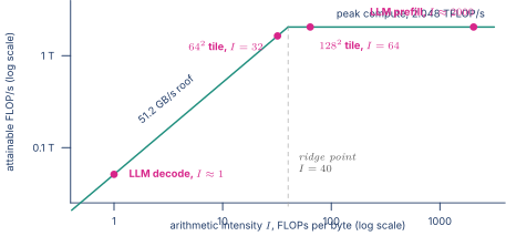
Apply it to the multiply from 1.1. At bf16, . Attainable performance is GFLOP/s, which is 3.3 percent of the machine's peak. You built 1024 multipliers and 33 of them are doing useful work. Nothing is broken. The memory system simply cannot feed the array.
And that is before you notice the fine print on the word "ideal." The 192-byte figure assumed every element was read exactly once, which requires holding all of , all of , and all of somewhere fast while you work. For that is trivially true. For in bf16 it is MiB, which does not fit in the 256 KiB scratchpad of Model Machine M and will not fit in the scratchpad of any accelerator you are likely to build.
So the real problem statement, the one the next seven parts answer, is this. Get the operand reuse of the ideal case without the storage of the ideal case. There are exactly two mechanisms. Reuse an operand across many arithmetic units in space, which is the systolic array of Part 2. And reuse a block of operands across many cycles in time, which is the tiling of Part 4. Real accelerators do both, at once, and the interaction between them is most of the design work.
02.Part 2, the systolic array, as an answer to a specific problem
2.1 The problem restated in bandwidth
Model Machine M has 1024 MACs. To keep them all busy, every cycle, the naive scheme needs operands delivered per cycle. In bf16 that is 4096 bytes per cycle, and at 1 GHz that is 4.1 terabytes per second out of the on-chip memory. On-chip SRAM is fast, but it is not that fast. A single SRAM macro of the kind SRAM Arrays and ECC describes delivers one access of perhaps 128 or 256 bits per cycle. You would need something like 128 to 256 independent banks, all conflict-free, feeding a crossbar with 2048 endpoints. The crossbar alone would be larger and burn more power than the multipliers it serves, and its wires would set the clock period rather than the arithmetic doing so.
So the question is not "how do I build 1024 multipliers." Multipliers are easy. The question is how do I arrange 1024 multipliers so that they need far fewer than 2048 new operands per cycle.
2.2 One cell, then the wiring
Start with one cell. A MAC cell holds a running sum in a register. Each cycle it takes an value and a value, forms , adds it to the register, and writes the register back.
| psum <= psum + (a * b); |
That is one line of RTL and about the simplest useful datapath there is. Now add two more registers, one that captures and one that captures , and drive the cell's right-hand neighbour from the register and its downstairs neighbour from the register.
| a_out <= a_in; // pass activation to the right | |
| b_out <= b_in; // pass weight downward | |
| psum <= psum + a_in * b_in; |
Three registers, one multiplier, one adder. Every wire leaving the cell goes to a physically adjacent cell, and no wire is longer than one cell pitch. That last property is not a detail. It is the reason the structure exists, and it is a physical-design argument as much as a microarchitectural one, in the sense of STA Synthesis and Physical Design. A design whose only wires are nearest-neighbour has no long routes, no route-dependent skew, one repeatable timing arc replicated a thousand times, and a layout you place once and array.
Now tile that cell into a grid.
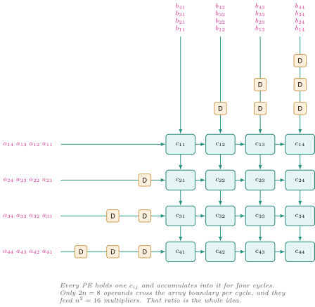
The name is systolic array, coined by H. T. Kung and Charles Leiserson around 1978, by analogy with the heart. Data is pumped through the structure in rhythmic beats, and each beat every cell does a little work on whatever arrived and passes it along. The version drawn above, where each cell owns an output element, is output-stationary, which Part 3 puts in context.
2.3 Marching the numbers through, cycle by cycle
Take the exact and from 1.1 and run them.
PE needs to see the pairs , then , then , then , in that order, on four consecutive cycles. But has to travel through cells to the left of PE to get there, and has to travel through cells above it. Each hop costs a cycle. So the operands only meet if they are launched at the right times, and the fix is to delay row of by cycles and column of by cycles before they enter. Those are the triangular chains of D registers on the two edges of the drawing.
Here is the resulting feed schedule, which is the whole thing made concrete. A dash means nothing is entering that edge that cycle.
| cycle | row 1 in | row 2 in | row 3 in | row 4 in | col 1 in | col 2 in | col 3 in | col 4 in |
|---|---|---|---|---|---|---|---|---|
| 0 | – | – | – | – | – | – | ||
| 1 | – | – | – | – | ||||
| 2 | – | – | ||||||
| 3 | ||||||||
| 4 | – | – | ||||||
| 5 | – | – | – | – | ||||
| 6 | – | – | – | – | – | – |
Follow PE, the top-left corner, which sees operands with no delay at all.
| cycle | arriving | arriving | product | running psum |
|---|---|---|---|---|
| 0 | 1 | 1 | 1 | 1 |
| 1 | 2 | 0 | 0 | 1 |
| 2 | 0 | 3 | 0 | 1 |
| 3 | 1 | 1 | 1 | 2 |
Two, which is . Now follow PE, which is one row down and two columns right, so it starts at cycle .
| cycle | arriving | arriving | product | running psum |
|---|---|---|---|---|
| 3 | 0 | 0 | ||
| 4 | 1 | 1 | ||
| 5 | 0 | 1 | ||
| 6 | 0 | 1 |
One, which is , matching the hand calculation in 1.1. The bottom-right PE starts at cycle 6 and finishes at cycle 9, so the whole array is done after 10 cycles. In general an output-stationary array reducing over terms finishes in cycles, which for is .
Notice what never happened. No cell ever addressed a memory. No cell ever needed to know its own coordinates. There is no crossbar, no arbiter, and no control beyond a global "go" and a counter. The correctness of the whole thing is carried entirely by the geometry and by the delay registers.
2.4 What the geometry bought, counted
In steady state the array consumes values of and values of per cycle at its two edges, and performs MACs per cycle. So
For that is 2. For the array of Model Machine M it is 16. For the arrays that AWS documents in the NeuronCore tensor engine, or the array in Google's first-generation TPU as described in the ISCA 2017 paper, it is 64 and 128 respectively. Compare the naive scheme's 0.5 MACs per operand and the improvement factor is exactly .
Concretely for Model Machine M, instead of 2048 operands per cycle, the array needs 64, at 128 bytes per cycle, or 128 GB/s out of the scratchpad. That is one wide SRAM read per edge per cycle. The bandwidth problem that looked impossible in 2.1 is now routine, and the entire change was a wiring decision.
This is also the honest answer to "why not just build a big SIMD unit," which is what Execution Units and Vector Microarchitecture describe. A SIMD lane array reads all of its operands from a register file every cycle, so it needs the full width of operand bandwidth and pays for a big multi-ported register file to supply it. The systolic array replaces most of that register file bandwidth with short wires between neighbours. That is the trade, stated in one sentence. A systolic array converts register-file read ports into nearest-neighbour wires.
2.5 The costs, which is where interviews actually go
Three costs, and naming all three is what separates having thought about this from having read a blog post about it.
Fill and drain. The array is not full for the first cycles nor the last . Efficiency over one pass reducing terms is
For a array with , that is percent. Two thirds of the machine's cycles are spent filling and draining. Push to 4096 and it becomes percent. Large arrays demand long reduction dimensions, and if the workload does not have one you have bought silicon you cannot use. In practice the fill and drain of consecutive tiles can be overlapped, so the loss is smaller than the formula suggests, but only if the control was designed to do that, and that overlap is exactly the kind of thing that turns out to be missing in the first RTL.
Shape mismatch. An array natively computes an output tile. Give it a problem on a array and PEs out of 65,536 do work. That is 0.4 percent utilisation, and it is not a rounding error, it is a factor of 256. This is the single most important practical fact about big systolic arrays, and it is why the industry drifted from one enormous array toward many smaller ones, or toward arrays that can be partitioned. Meta's published MTIA v1 description, for instance, is an grid of 64 independent processing elements each with its own local SRAM and its own small matrix engine, rather than one monolithic array, and the flexibility argument is exactly this one.
Latency. A result is not available until the last accumulation reaches its PE, and then it must be drained out. Be precise about which number is late. The corner PE nearest the edges sees its first operand pair on cycle zero and has its answer after cycles. It is the far corner that waits cycles just to start. For a array that skew is cycles of pure fill and drain sitting on top of the cycles of actual reduction, so the tile is not complete until hundreds of cycles after it would have been on a machine with no geometry. For throughput workloads nobody cares. For a latency-sensitive single query it matters, which is precisely why MLPerf's inference rules distinguish a single-stream scenario measured at 90th-percentile latency from an offline scenario measured in raw throughput. A design that wins one can lose the other.
03.Part 3, the dataflow taxonomy
This is the classic interview question in the domain. It is asked at Google, at Meta, at Annapurna, and at every startup, and it is asked because the answer separates people who can recite three names from people who can say what each one minimises and what it pays.
3.1 What the word "stationary" actually refers to
Write the matrix multiply as its loop nest, with nothing hidden.
| for (m = 0; m < M; m++) // output row | |
| for (n = 0; n < N; n++) // output column | |
| for (k = 0; k < K; k++) // reduction | |
| C[m][n] += A[m][k] * B[k][n]; |
Three loops, three data structures, and each data structure is independent of exactly one loop index. does not depend on . does not depend on . does not depend on . That is the entire mathematical content of the dataflow taxonomy, and everything else follows from it.
If a value does not depend on a loop index, then as that loop runs the value does not change. So if you arrange for that loop to run inside a single hardware cell, the value can sit in a register in that cell and be read for free, over and over, instead of being fetched.
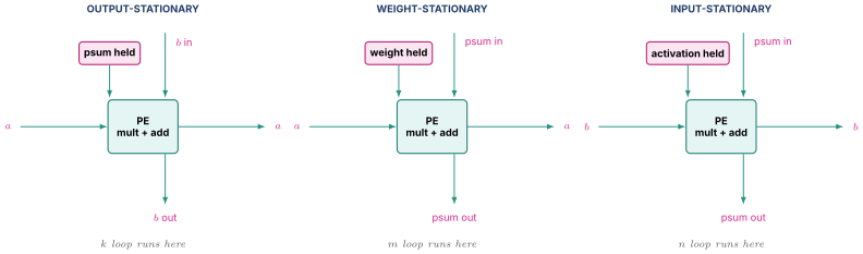
A dataflow is a choice of which of those three loops is executed inside the cell. Three choices, three names.
- Run the loop inside the cell and stays put. That is output-stationary.
- Run the loop inside the cell and stays put. That is weight-stationary, because in a neural network is the weight matrix and indexes the batch or the row of activations.
- Run the loop inside the cell and stays put. That is input-stationary or activation-stationary.
That is it. The names sound like folklore and they are actually just "which loop did you put innermost."
3.2 Output-stationary, and what it minimises
The array of Part 2 was output-stationary. PE owns and accumulates into it for all cycles.
What it minimises is partial-sum traffic. A partial sum is written once, at the very end. Never fetched, never spilled, never re-read.
That matters far more than it sounds, because of a width asymmetry that people forget. In an int8 network the inputs are 1 byte each and the accumulator is 4 bytes. In a bf16 network the inputs are 2 bytes and the accumulator is 4. The partial sum is the widest thing in the datapath, by a factor of two to four, so a byte of psum traffic saved is worth two to four bytes of input traffic saved. Output-stationary is the dataflow that refuses to move the expensive operand.
What it pays is that both inputs must arrive every cycle. The array boundary must sustain values of and values of per cycle, forever. There is no way to amortise either one.
It wins when , the reduction dimension, is long. Cost the array-edge traffic for an array over steps. It reads values of and values of , and writes psums, so traffic is elements. As grows, that lone term becomes free. Deep convolutions and transformer projections both have long . A weight matrix has .
3.3 Weight-stationary, and what it minimises
Now PE holds a weight and keeps it for the entire pass. Activations enter from the left and flow right. Partial sums enter at the top of each column and flow down, growing as they go, so that the value emerging from the bottom of column has accumulated one product from each of the PEs in that column. The reduction happens in space, along the column, rather than in time inside a register.
The first-generation Google TPU is the canonical published example. The ISCA 2017 paper describes a array of 8-bit MACs running at 700 MHz for a peak of 92 tera-operations per second, with weights loaded into the array from above and held while activations stream through and partial sums propagate. The literature classifies that as weight-stationary.
What it minimises is weight fetch. Load weights once, then stream rows of activations through them. Traffic is elements, and as grows, the weight load becomes free.
What it pays is that partial sums move every cycle, and they are the wide operand. Every column carries a growing psum through adders, which also means the accumulator adder is on a path that must be sized for the full accumulator width at every stage.
It wins when , the batch or activation-row dimension, is long relative to the array. Training with a batch of 512, or inference on a large batch of images, is exactly that. This is why weight-stationary dominated the first generation of datacenter inference chips, where batching was free.
It loses catastrophically when . Load weights, perform MACs, and throw the weights away. One MAC per weight fetched, which is zero reuse. Section 7.5 shows that is exactly the shape of large-language-model token generation, and this is one honest way to state why decode is so hard. In dataflow terms, the batch dimension that weight-stationary needs to amortise its weight load has collapsed to one.
3.4 Row-stationary, and why it is a different kind of answer
The first three are symmetric. Pick a data type, minimise its traffic. Row-stationary, introduced with the Eyeriss chip by Chen, Emer and Sze at ISCA 2016, does something categorically different. It does not minimise the traffic of any one operand. It minimises total energy across all three, and it does so by mapping a different primitive into the PE.
The primitive is a one-dimensional convolution. Each PE holds one row of filter weights and streams one row of input activations past it, producing one row of partial sums. Within the PE, the filter row is reused across every position of the sliding window, the activation row is reused across every filter tap, and the partial sums accumulate locally. All three data types get reuse inside one PE, which none of the stationary-by-type dataflows achieve.
The two-dimensional array then handles the second convolution dimension. PEs in a diagonal share the same filter row, PEs in a row share the same activation row, and PEs in a column accumulate psums for the same output row, so reuse continues between PEs, over the short nearest-neighbour links, without touching the global buffer.
The reason to care is an energy table, and the published Eyeriss figures put it starkly. Taking one MAC operation as the unit, a read from the PE's own register file costs about 1, a hop to a neighbouring PE about 2, an access to the on-chip global buffer about 6, and a DRAM access about 200. Treat those as order-of-magnitude and process-specific rather than as constants of nature, but the shape is not in doubt. The arithmetic is nearly free and the data movement is the entire energy budget. A dataflow that keeps 90 percent of accesses in the register file and the neighbour links, even at the price of slightly more total accesses, wins on joules by a wide margin.
What it pays is complexity. The mapping from a layer's shape onto the array is intricate, the control is far more involved than a counter, and the whole scheme is shaped around convolution. Fully connected layers and transformer matrix multiplies, which have no sliding window at all, do not benefit from the convolutional reuse row-stationary is built to exploit. That is a real limitation in 2026, when the workload mix has moved heavily toward transformers.
3.5 The comparison, and how to answer the question out loud
| holds in the PE | minimises | pays | wins when | |
|---|---|---|---|---|
| Output-stationary | the partial sum | psum traffic, the widest operand | both inputs delivered every cycle | reduction is long |
| Weight-stationary | one weight | weight fetch from memory | psums move and are wide | batch or row count is long |
| Input-stationary | one activation | activation fetch | psums move, weights stream | one activation feeds many filters, and weights are cheap to stream |
| Row-stationary | a filter row and an activation row | total data-movement energy across all three | mapping and control complexity, convolution-shaped | convolutional layers on an energy-constrained part |
The sentence to have ready is this. Each dataflow amortises a fixed cost over the loop it runs inside the PE, so you choose the dataflow by asking which loop bound is largest in the layers you actually care about. Output-stationary amortises the psum write-out over . Weight-stationary amortises the weight load over . If is 4096 and is 1, output-stationary. If is 512 and is 64, weight-stationary. If it is a depthwise convolution on a phone and joules are the currency, row-stationary.
And the honest coda is worth volunteering. Real accelerators are not purely any of these. They are usually output-stationary at the PE level with a weight-stationary outer loop, or they are reconfigurable between two modes because the layer shapes in one network vary by two orders of magnitude. Saying "the taxonomy is a way to reason about the choice, not a menu you pick one item from" is a stronger answer than picking one.
04.Part 4, tiling a GEMM against an on-chip scratchpad
4.1 The matrices do not fit, so the loop nest must change
Part 1 established that ideal reuse requires holding everything on chip and that everything does not fit. Part 2 gave spatial reuse inside a array. That still leaves the traffic between DRAM and the on-chip memory unsolved, because the array only holds 1024 values at a time and the matrices hold millions.
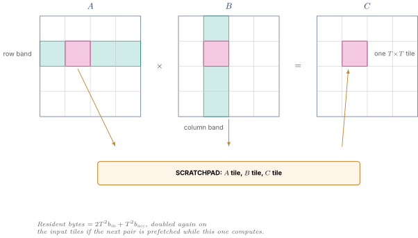
The fix is tiling, also called blocking. Cut each matrix into square blocks of size , and rewrite the loop nest so the inner three loops work entirely inside one block triple that is resident on chip.
for (i0 = 0; i0 < N; i0 += T)            // which C tile, row
 for (j0 = 0; j0 < N; j0 += T)           // which C tile, column
  for (k0 = 0; k0 < N; k0 += T) {        // which pair of A and B tiles
    load A[i0..i0+T][k0..k0+T] into scratchpad;
    load B[k0..k0+T][j0..j0+T] into scratchpad;
    for (i = i0; i < i0+T; i++)          // these three loops run
    for (j = j0; j < j0+T; j++)         // entirely on chip, and are
      for (k = k0; k < k0+T; k++)        // what the systolic array does
      C[i][j] += A[i][k] * B[k][j];
  }
Nothing about the mathematics changed. The same MACs happen in a different order. What changed is that each loaded tile is used times before it is discarded.
4.2 The traffic, worked
Count DRAM traffic for the tiled version, in elements.
The two outer loops visit output tiles. For each, the loop runs times, and each iteration loads one tile and one tile, which is elements. So
and is written once, elements. Arithmetic intensity is therefore
for large . That is the result the whole part exists for, and it is worth putting in a box in your head.
Arithmetic intensity is set by the tile size and by nothing else. Not by the matrix size, not by the number of MACs, not by the clock. The single decision that determines whether an accelerator is compute-bound or bandwidth-bound on GEMM is how big a tile fits on chip.
Check it against Part 1. Model Machine M has a ridge point of 40 FLOPs per byte. In bf16, , so compute-bound requires
4.3 The capacity calculation, which is what sizes the SRAM
Now go the other way. What does a tile size of demand in storage?
Three tiles must be resident: one of , one of , one of . Inputs are bf16 at 2 bytes. The accumulator tile is fp32 at 4 bytes, for the reasons Part 5 gives. So
But that number is wrong in practice, because if the DMA only starts fetching the next pair of tiles after the array finishes the current one, the array idles for the whole fetch. You want the fetch of tile pair to overlap the compute on tile pair , which means two copies of each input tile: one being read by the array, one being written by the DMA. That is double buffering, sometimes called ping-pong, and it is not optional on any real accelerator.
Now solve both directions on Model Machine M with its 256 KiB scratchpad.
| resident bytes | fits in 256 KiB? | vs ridge 40 | achieved fraction of peak | ||
|---|---|---|---|---|---|
| 32 | 12 KiB | yes | 16 | bandwidth-bound | 40 percent |
| 64 | 48 KiB | yes | 32 | bandwidth-bound | 80 percent |
| 96 | 108 KiB | yes | 48 | compute-bound | 100 percent |
| 128 | 192 KiB | yes | 64 | compute-bound | 100 percent |
| 192 | 432 KiB | no | 96 | – | – |
So is the design point. It is a power of two, comfortably above the threshold, and it fits with 64 KiB to spare for weights, descriptors, and the output tile staging. And the argument runs in reverse just as well, which is the version you want in an interview. If the roofline target says and the natural power of two is 128, then the scratchpad must be at least KiB, and that is where the SRAM budget number comes from. It is not a guess and it is not a round number somebody liked. It is a consequence of the DRAM bandwidth and the MAC count.
Sanity-check it a third way, in time rather than in bytes, because the three should agree. For , one step loads bytes, taking . The compute for that step is MFLOP, taking . Compute time exceeds load time, so with double buffering the DMA hides completely and the array never stalls. The ratio is exactly , the ridge point over the arithmetic intensity. Three independent routes, one answer. When your spreadsheet and your performance model and your RTL do not agree like that, one of them is wrong.
4.4 Why it is a scratchpad and not a cache
An accelerator's on-chip memory is almost always a scratchpad, a plain addressable SRAM with no tags, no valid bits, no replacement policy, no misses, and no hardware that decides anything. Software or a DMA engine puts data in it explicitly and takes data out explicitly. That is the opposite of the cache of Cache Organization and Prefetching, and the reasons are worth having straight.
The access pattern is known in advance. A cache exists because a CPU does not know what it will touch next. A GEMM knows its entire access sequence before the first cycle. Paying for tags, comparators, and replacement logic to predict something you already know is pure overhead. Tag arrays and their comparators are a meaningful fraction of a cache's area and a larger fraction of its energy per access.
Determinism. With a scratchpad the compiler can compute exactly when every byte arrives, so it can schedule the array to the cycle. With a cache, one unexpected miss stalls the array and the schedule is a distribution rather than a number. For a machine whose whole value proposition is keeping 1024 multipliers busy, a stall is expensive and an unpredictable stall is worse.
Banking for width. The array needs 32 values of and 32 of every cycle. A single SRAM macro delivers one access per cycle, perhaps 256 bits wide, which is 16 bf16 values. So you need at least four banks, and in practice more, with an address mapping chosen so the array's natural stride never puts two simultaneous accesses in the same bank. That kind of hand-designed conflict-free banking is straightforward on a scratchpad and awkward on a cache, whose bank mapping is dictated by the address bits.
What you give up is real and should be said. Software, or the DMA descriptor stream, now owns correctness of data placement. There is no hardware backstop. If the compute reads a scratchpad region before the DMA finished writing it, you get stale data silently, with no miss, no exception, and no coherence protocol to save you. That is the single most common class of bug in accelerator bring-up, it is a race between two engines rather than a logic error, and Part 8 and Part 9 both come back to it because it is the thing an assertion should catch.
Public designs bear this out. NVDLA, the open-source NVIDIA Deep Learning Accelerator whose full RTL and specification are published, is built around an explicitly managed convolution buffer feeding a MAC array, not a cache. AWS documents the NeuronCore's on-chip SBUF and PSUM as software-managed state spaces addressed by the compiler. Meta's MTIA v1 description gives each of its 64 processing elements 128 KiB of local SRAM with a large on-chip pool behind it. Different companies, same architectural decision.
05.Part 5, the numeric formats, from what a float is
5.1 A floating-point number, built from nothing
Start below the beginning. A fixed number of bits can represent a fixed number of distinct values, and the only question is which values you choose. Fixed point spaces them evenly. With 8 bits you might choose , and every gap is 0.01. Floating point spaces them logarithmically, so the gaps near zero are tiny and the gaps near the maximum are enormous, which buys enormous range at the cost of uniform precision.
The construction is scientific notation in binary. A number is stored as three fields.
The sign is one bit. The exponent field is an unsigned integer from which a fixed bias is subtracted so that negative exponents can be stored, and the bias is always for a -bit exponent field. The mantissa or significand field holds the fractional bits after an implied leading 1, which is free precision. Every normalised binary number starts with a 1, so there is no point storing it.
Work one encoding completely. Represent in fp32.
Convert to binary. and , so . Normalise by sliding the point left two places to get . So the true exponent is 2, and with fp32's bias of 127 the stored exponent field is . The mantissa field holds the bits after the leading 1, which is , padded with zeros to 23 bits. Sign is 0.
Reverse it as a check. , and . Correct.
Two derived quantities decide everything about which format to use for what.
Dynamic range is set by the exponent width alone. The largest finite value is roughly and the smallest normal value is , so the ratio between them is roughly . Eight exponent bits give a range of about , five give about , four give about .
Precision is set by the mantissa width alone. With stored mantissa bits the spacing between neighbouring representable values is relative to the value, so the worst-case relative rounding error is .
They are independent, they trade against each other for a fixed total width, and the last decade of machine-learning number formats is a single long argument about where to put the boundary.
5.2 The formats side by side
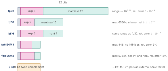
| format | // | bias | max finite | min normal | worst relative error |
|---|---|---|---|---|---|
| fp32 | 1/8/23 | 127 | |||
| fp16 | 1/5/10 | 15 | 65504 | ||
| bf16 | 1/8/7 | 127 | |||
| fp8 E4M3 | 1/4/3 | 7 | 448 | ||
| fp8 E5M2 | 1/5/2 | 15 | 57344 |
5.3 Why bf16 exists at all, which is the exponent-range argument
fp16 came first, standardised in IEEE 754-2008, and it was designed for graphics, where values live in a narrow band around one. Training a neural network revealed that its five exponent bits are not enough, and the reason is worth working numerically rather than asserting.
During training, the quantity that flows backward through the network is a gradient, and gradients get small. Multiply a chain of thirty layers each contributing a factor around 0.5 and you are at before anything unusual has happened.
Take a gradient value of and try to store it.
In fp16, the smallest normal value is . Below that there are subnormals down to . And is smaller than that. It flushes to exactly zero. The gradient does not become imprecise. It ceases to exist. The weight it was going to update never updates, and the network stops learning in that direction, silently, with no error, no NaN, and no warning.
In bf16, the smallest normal value is . A value of sits thirty decimal orders of magnitude above that floor, which is very nearly a hundred binades, nowhere near trouble.
Now the other end. During training you also compute sums of squares, and those get large. A value of squared is , which overflows fp16 to infinity at 65504, and once one infinity appears it contaminates everything downstream through the first subtraction that produces a NaN. In bf16, is unremarkable.
So the argument for bf16 is not that it is more accurate. It is strictly less accurate than fp16, with 8 significand bits against 11, and saying otherwise in an interview is the standard trap in this question. The argument is that neural networks turn out to be robust to imprecision and fragile to range. Being 0.4 percent wrong about a gradient is harmless because the next mini-batch corrects it and stochastic gradient descent is a noisy process anyway. Being zero about a gradient is a permanent loss of information.
There was a workaround for fp16 and it is worth knowing because it explains why bf16 won. Loss scaling multiplies the loss by a large constant, say , before backpropagation so that all gradients shift up into fp16's representable band, then divides the weight updates back down. It works, but it requires a dynamic controller that watches for overflow, backs the scale off, and retries the step, which is software complexity in the innermost loop of training and a source of hard-to-reproduce failures. bf16 makes the problem not exist.
And bf16 has a second property that made hardware people love it, which is worth volunteering because it is a hardware argument rather than a numerics argument. bf16 is fp32 with the bottom 16 bits deleted. Same exponent width, same bias. So conversion between the two is a truncation in one direction and a zero-pad in the other, with no exponent re-biasing, no range check, and no possibility of overflow or underflow. A bf16 to fp32 converter is a wire.
The area argument closes it. The dominant cost in a floating-point multiplier is the significand multiplier, whose area grows roughly as the square of its width. Counting the implied bit, fp32 needs , fp16 needs , and bf16 needs .
| significand multiply | relative array area | |
|---|---|---|
| fp32 | ||
| fp16 | ||
| bf16 |
So a bf16 multiplier array is roughly half the size of an fp16 one and roughly an order of magnitude below fp32. That is the partial-product array only, ignoring exponent handling, alignment, normalisation, and rounding, which do not scale the same way, so treat it as the shape of the argument rather than a synthesis result. But it is why, at a fixed area budget, you can build about nine times as many bf16 multipliers as fp32 multipliers, and that factor of nine is the reason reduced precision exists.
5.4 fp8, and the two shapes it comes in
Below 16 bits the exponent-versus-mantissa argument gets sharp enough that one format is not enough, and the Open Compute Project's OFP8 specification standardises two.
E4M3 has 4 exponent bits and 3 mantissa bits, with a bias of 7. It gives up the ability to represent infinities and uses only two bit patterns for NaN, which lets it reclaim the all-ones exponent code for finite numbers and push its maximum to 448 rather than 240. Range is small. Precision, at 4 significand bits, is the best 8-bit float can do.
E5M2 has 5 exponent bits and 2 mantissa bits, bias 15, and keeps infinities and NaNs. Its exponent field is identical to fp16's, so its dynamic range is the same as fp16's, roughly . Its precision is 3 significand bits, meaning a worst-case relative error around 12 percent.
The division of labour that has settled in practice is E4M3 for weights and activations in the forward pass, where values are well-conditioned and precision matters, and E5M2 for gradients, where the dynamic range problem of 5.3 reappears in an even sharper form. Both are usually paired with a per-tensor scale factor in a wider format, so the fp8 values only have to cover the spread within a tensor and the scale carries the tensor's overall magnitude. That combination is the same idea as int8 quantisation in Part 6, applied to a float, and the microscaling formats standardised more recently push it further by attaching a shared exponent to every small block of elements rather than to a whole tensor.
5.5 The accumulator, which is the question nobody expects
Here is the part that separates arithmetic-hardware people from everybody else, and it is asked constantly because it has a numeric answer.
You never accumulate in the input format.
Take bf16, with 8 significand bits. Accumulate 1024 values, each equal to 1.0, in bf16. Everything is fine until the running sum reaches 256. At , the spacing between representable bf16 values is . So is not representable, and round-to-nearest-even sends it back to 256. The sum sticks at 256 and never moves again, no matter how many more ones you add. You asked for 1024 and you got 256, an error of 75 percent, with no exception raised.
Here is the general form. Accumulation stagnates once the running sum reaches times the addend, where is the stored mantissa width, because at that value one unit of the addend is exactly half a step and round-to-nearest-even sends the tie back down.
| accumulate format | stagnation point for unit addends | |
|---|---|---|
| fp8 E4M3 | 3 | 16 |
| bf16 | 7 | 256 |
| fp16 | 10 | 2048 |
| fp32 | 23 | 16.8 million |
So the rule in every accelerator built in the last decade is multiply in the narrow format, accumulate in fp32. The asymmetry that makes that cheap is a scaling argument, and it is worth stating as one rather than asserting that accumulators are free. A multiplier's partial-product array grows as the square of its operand width, which is the against comparison of 5.3, so every bit removed from the multiplier's inputs is worth a great deal. An accumulator is a register and an adder, and both grow only linearly in width. Widening the multiply from 8 significand bits to 24 costs roughly nine times the array area. Widening the accumulator from 16 bits to 32 costs roughly twice a much smaller number. You are trading a quadratic cost for a linear one, in the direction that makes the quadratic one small. This is called mixed precision and it is not a compromise, it is the correct design.
The integer version has a cleaner answer. int8 times int8 gives a product bounded by , which needs 15 bits. Summing of them needs bits.
| max magnitude | bits needed | |
|---|---|---|
| 64 | 21 | |
| 256 | 23 | |
| 1024 | 25 | |
| 4096 | 27 |
An int32 accumulator has room for accumulations, so int32 simply cannot overflow for any real layer, which is why it is universal. It is also worth noticing that it is overkill. If your hardware bounds at 1024, the table above says 25 bits carries every representable sum, so a 26-bit accumulator with a guard bit is already generous, and against int32 that saves six bits of flip-flop and six bits of adder in every cell. On a 1024-MAC array that is roughly six thousand flops plus the adder logic, which is a real area line item worth raising in a PPA discussion, offset against the loss of generality if a future layer wants a longer reduction. The right answer is usually "size it for the architectural maximum and state that maximum in the specification," and stating it is the part people forget.
06.Part 6, quantisation
6.1 The mapping, worked on eight numbers
Quantisation is the mapping from a set of real numbers to a set of integers, plus enough metadata to get back. Everything else is bookkeeping.
Take eight weights.
The simplest scheme, and the one used for weights almost universally, is symmetric. Find the largest magnitude, map it to the largest representable integer, and scale everything else linearly. The largest magnitude here is 0.90, and signed int8 goes to 127, so the scale is
and the quantised value of a real is , clamped to .
| real | dequantised | error | ||
|---|---|---|---|---|
Largest error is 0.00354, which is exactly half a step, as it must be for round-to-nearest. The eight numbers now occupy 8 bytes instead of 32, and every multiply involving them is an 8-bit integer multiply rather than a 32-bit float multiply.
The reason this is a hardware topic rather than a software topic is the identity that makes it work in an array.
The scales factor out of the sum. So the array does pure integer MACs into an int32 accumulator, knowing nothing about scales, and one multiplication by at the very end recovers the real answer. If that factoring did not hold, integer arrays would be useless, and section 6.4 shows exactly which design choice breaks it.
6.2 Asymmetric, and the zero point
Weights are roughly symmetric about zero, so the scheme above wastes nothing. Activations after a ReLU are not. They are all non-negative. Map symmetrically into int8 and you use only , throwing away the entire negative half of the range, which is one whole bit of precision.
Asymmetric quantisation fixes it with a second parameter, the zero point , an integer that says which quantised code represents real zero.
For the range mapped onto the full signed int8 span, which is 256 codes and therefore 255 steps between the endpoints, and , so code means 0.0 and code means 6.0. You recovered the bit.
The cost lands squarely in the hardware, and it is the follow-up question. Expand the dot product with zero points on both operands.
Four terms. The first is the ordinary integer MAC. The third and fourth involve only weights and constants, so they are computed once at compile time and folded into the bias. The second term is the problem. It needs the sum of the activations along the reduction axis, which is data-dependent and only known at run time. The hardware must provide it, either as an extra accumulator column that sums activations in parallel with the main array, or as a separate pass. That is real silicon, spent purely to support a non-zero activation zero point.
Which is why the common industrial compromise, written down explicitly in the published LiteRT 8-bit quantisation specification and matched by the ONNX Runtime default, is symmetric weights and asymmetric activations. Setting deletes the second term entirely, because multiplies it. You keep the extra bit of activation precision and you pay nothing for it.
Worth knowing that the compromise is not universal, because an interviewer may push on it. NVIDIA's TensorRT documentation states that its quantisation scheme is symmetric on both sides, weights and activations, so the zero point is implicitly zero everywhere and the dequantisation is a single multiply. That choice deletes all three correction terms rather than one, at the cost of the activation precision bit that asymmetry was buying. Naming both conventions, and the reason each is defensible, is a better answer than asserting one is standard.
6.3 Per-tensor against per-channel, with the failure worked
A convolution or linear layer has many output channels, and each output channel has its own filter. Nothing forces those filters to have similar magnitudes, and in trained networks they routinely do not, because batch normalisation and weight decay leave some channels doing heavy lifting and others contributing very little.
Suppose a layer has 64 output channels. Channel 0's weights span . Channel 37's weights span .
Per-tensor quantisation gives the whole weight tensor one scale, set by the largest magnitude anywhere in it, so . Now quantise channel 37's largest weight.
Channel 37's entire filter is now made of the values , , and . It has been reduced to a ternary filter. The information lost is bits, so a nominally 8-bit quantisation has delivered about 1 bit to that channel. The layer's output on that channel is garbage, and because it is one channel out of 64, the aggregate accuracy metric drops by a puzzling couple of percent that nobody can localise.
Per-channel quantisation gives each output channel its own scale. Channel 37 gets and its weights use the full int8 range with the same relative precision as every other channel. The metadata cost is 64 scale values instead of one, which for a layer holding hundreds of thousands of weights is nothing.
This is not a subtle effect and it is not controversial. Per-channel weight quantisation is the default in essentially every production int8 flow, and if a candidate says "we just use per-tensor everywhere" the follow-up will be about exactly this failure.
6.4 What the hardware must provide, and the trap in the axis
Three things, and one thing you must refuse to provide.
An int32 accumulator per output element. Established in 5.5.
A requantisation stage between the accumulator and the output. The int32 accumulator must be scaled by and written back as int8 for the next layer. is a real number less than one, and hardware does not divide. So express it as a fixed-point value, with a 16- or 32-bit integer representing a fraction in , precomputed offline. At run time the hardware does one integer multiply by , one rounding right shift by , then adds the output zero point and saturates to int8. That is a multiplier, a shifter, an adder, and a clamp, per output lane, and it is a whole pipeline stage in the design.
A per-channel scale table. With per-channel quantisation, and differ per output channel, so the requantisation stage needs a small memory indexed by output channel, loaded when the layer's weights are loaded. Small, but it is a structure that has to exist, be filled by the DMA, and be sequenced correctly relative to the compute.
And now the trap, which is a genuinely good interview question because the wrong answer sounds reasonable.
Per-channel along which axis?
Go back to the identity in 6.1. It worked because was a constant with respect to , the reduction index, so it came outside the sum. Per-output-channel quantisation indexes the scale by , the output column, which is not , so the factoring still holds and the scale is applied once at the end. Free.
Per-input-channel quantisation would index the scale by . Then
and does not come out of the sum. Every single MAC would need its own scale multiply, inside the array, on the critical path, in floating point. The integer array is destroyed. So the rule is exact and worth memorising in this form. You may quantise per-channel along any axis you like except the reduction axis, because only the reduction axis is inside the sum.
The same logic explains block or group quantisation, where a scale is shared by every 32 or 64 elements along the reduction axis. That does put a scale inside the sum, so the hardware handles it by breaking the reduction into blocks. Accumulate 32 products in integer, apply that block's scale, add into a wider running accumulator, repeat. It is a real technique and it is the basis of the microscaling formats, but it costs a scale-apply stage every 32 accumulations, and that cost is the honest thing to name when asked why block sizes are 32 and not 4.
07.Part 7, transformers and LLM inference, as a hardware workload
7.1 What the model is, mechanically
Strip away everything about language. A transformer is a stack of identical layers operating on a sequence of vectors.
A token is a chunk of text, roughly three quarters of a word on average. Each token is turned into a vector of numbers, called its embedding, where is typically 2048, 4096, or 8192. A sequence of tokens is therefore a matrix, and that matrix is the only thing that flows through the model.
Each layer does two things to it, in order.
Attention lets every token look at every other token and pull in information from the ones that matter. This is the part with interesting hardware consequences and 7.2 works it by hand.
The feed-forward block, sometimes MLP, applies the same two-matrix transformation to each token independently. It is , a nonlinearity, then , where is and is . Nothing subtle. It is two GEMMs, and it holds roughly two thirds of the model's parameters.
Both blocks are matrix multiplies. A "70-billion-parameter model" means the total element count of all those weight matrices across all layers is . Everything Parts 1 through 6 built applies directly.
7.2 Attention, worked on three tokens
The mechanism is easier than its reputation. Each token produces three vectors by three separate matrix multiplies against learned weights: a query meaning "what am I looking for," a key meaning "what do I offer," and a value meaning "what I will hand over if chosen."
Take a sequence of three tokens with , and to keep the arithmetic visible take the three projection matrices to be the identity, so .
Step one, scores. Every query dots with every key, scaled by .
The exists so that the dot product's magnitude does not grow with and push the softmax into saturation. It is a numerics fix, and it matters to hardware only in that it is one more scalar multiply in the pipeline.
Step two, causal mask. In a language model a token may only attend to itself and to tokens before it, because at generation time the later ones do not exist yet. So everything above the diagonal is set to , which becomes zero after the exponential.
Step three, softmax. Convert each row into weights that are positive and sum to one, by exponentiating and normalising.
Row 1, only entry 1 survives, so weights are .
Row 2, entries . , , sum 3.028, so weights are .
Row 3, entries . twice and , sum 8.169, so weights are .
Step four, weighted sum of values.
That is attention, completely. Two matrix multiplies with a softmax between them.
The hardware consequences fall out immediately. The score matrix is , so its size grows quadratically in sequence length, and at that is a billion entries per head per layer, which cannot be materialised. That is the entire motivation for the streaming attention algorithms that compute the softmax incrementally without ever holding the full score matrix, which is a software technique with a hardware requirement. The accelerator needs enough on-chip storage and enough flexibility in its reduction hardware to run a running-maximum and running-sum alongside the matrix multiply. And softmax is not a matrix multiply. It needs an exponential, a maximum, a reciprocal, and two reduction passes. Every accelerator therefore has a vector or special-function unit sitting beside the matrix engine, and how well the two overlap is a real performance question. The AWS NeuronCore documentation, for instance, describes exactly this split: a tensor engine for the systolic matrix work, plus vector, scalar, and general-purpose SIMD engines alongside it.
7.3 The KV cache, and why it exists
Generation is sequential. The model produces one token, appends it to the sequence, and runs again to produce the next.
Look at what happens on step . The new token produces , and to compute its attention output it needs the keys and values of every previous token. But through depend only on tokens 1 through , which have not changed. Recomputing them would cost the full key and value projections for the entire prefix, every single step, which turns generation of tokens into projection work.
So you store them. The KV cache holds every key and value vector for every token, every layer, and every head, and it is read in full on every generation step.
Size it. Take a model with layers, , and ordinary multi-head attention where the keys and values are the full wide, stored in fp16.
The leading 2 is for keys and values. Half a megabyte per token. At a 4096-token context that is 2 GiB. Serve eight concurrent users and the KV cache alone is 16 GiB, which for a 7-billion-parameter model stored in fp16 at 14 GB is larger than the model.
Two mitigations you should know by name. Grouped-query attention shares one key-value pair across a group of query heads. With 32 query heads but only 8 key-value heads, the cache shrinks by exactly , to 128 KiB per token, at a small and empirically acceptable quality cost. And KV cache quantisation stores keys and values in int8 or fp8 rather than fp16, halving or quartering it again. Both exist because the KV cache, not the weights, is what limits how many users a serving system can hold.
7.4 Prefill, which is compute-bound
Generation has two phases with completely different hardware character, and confusing them is the most common mistake in this area.
Prefill processes the entire input prompt at once. All tokens go through the model together, so every matrix multiply is a genuine matrix-by-matrix product with rows.
Cost it for a 7-billion-parameter model, , , prompt length .
The weight arithmetic is two FLOPs per parameter per token:
The attention-specific arithmetic, which is the and the value-weighted sum and does not involve weights at all, is :
so about 7 percent of the total at this length. The two terms are equal when , that is when
which is a useful thing to be able to derive. Below roughly 27,000 tokens the weights dominate, above it the quadratic attention term does, and that crossover is why long-context serving is a different engineering problem from ordinary serving.
Now the bytes. The weights are read once for the whole prompt, GB in fp16.
Two thousand. Against a ridge point of 40 on Model Machine M, or a few hundred on a large datacenter part, prefill is deeply compute-bound. It is the best-behaved workload a matrix engine will ever see, it will run near peak, and if it does not, the problem is your tiling.
7.5 Decode, which is bandwidth-bound, and by how much
Decode produces one token at a time. Every matrix multiply now has exactly one row.
A matrix multiply with one row is not a matrix multiply, it is a matrix-vector product, and everything in Parts 1 through 4 collapses. Go back to the intensity formula with . You read a weight matrix and perform MACs, so you get exactly one MAC per weight element fetched, and no amount of tiling, dataflow selection, or array size changes that, because there is no reuse to find. The weight is used once by definition.
Cost one decode step on the same model, with 2048 tokens already in context.
The arithmetic is GFLOP, plus attention over the cache GFLOP. Call it 15 GFLOP.
The bytes are the entire weight set, 14 GB, plus the entire KV cache, GB. Call it 15 GB.
One. Prefill was 2050. Same model, same weights, same silicon, and the arithmetic intensity differs by a factor of two thousand.
Turn it into a time. On a machine with 1 TB/s of memory bandwidth, one decode step takes at minimum
giving about 67 tokens per second, and that is a hard floor imposed by bandwidth alone. If the same machine has 400 TFLOP/s of compute, the arithmetic would take . The matrix engine is doing useful work for 0.25 percent of the wall clock and waiting for memory for the other 99.75 percent.
Three consequences, and they are the things a hardware engineer says next.
Adding MACs does nothing. Doubling the array doubles the 0.25 percent to 0.5 percent. This is the trap in the question "how would you speed up token generation," and the answer "more compute" is wrong in a way that is easy to demonstrate.
Batching is the lever, and it works because it manufactures reuse. Serve requests at once and the weights are fetched once and used times, so . To reach a ridge point of 400 you need a batch around 400, which is why production serving systems batch as aggressively as latency budgets allow and why continuous or in-flight batching, which lets requests join and leave a running batch, was such a large practical win. The ceiling on this is the KV cache. It is per-request, so its traffic scales with and does not amortise. Batching amortises the weights and not the cache, which is precisely why grouped-query attention and cache quantisation matter so much.
The other levers are all about reading fewer bytes. Weight quantisation to int8 or fp8 halves or quarters the 14 GB. Sparsity skips bytes entirely if the hardware can address them. Speculative decoding runs a small cheap model to guess several tokens and then verifies them with one pass of the big model, converting several sequential memory-bound steps into one step with several rows, which is batching in the time dimension.
The design conclusion is the uncomfortable one, and it is worth stating plainly because it explains a lot of industry behaviour. Prefill and decode want different machines. Prefill wants a huge array and modest bandwidth. Decode wants enormous bandwidth and cares little about the array. Building one chip that does both well means either overprovisioning one resource or partitioning the fleet, and disaggregated serving, where prefill and decode run on separate machines, exists because of exactly this arithmetic.
7.6 Where the benchmarks come in
The industry-standard way to compare all of this is MLPerf, run by MLCommons, and a hardware engineer should know its shape because it is the number that ends up on the slide.
It splits into training and inference suites. Inference defines four scenarios, and they map onto the phases above. Single-stream sends one query at a time and reports a 90th-percentile latency, which is the phone and the interactive case. Multi-stream sends a fixed number of concurrent queries. Server models random arrivals against a latency bound, which is the realistic datacenter serving case and the one where the prefill-decode tension bites. Offline sends everything at once and reports pure throughput, which is the friendliest possible case for a big array.
It also splits into a closed division, where you must run the reference model with the reference preprocessing so the comparison is genuinely apples to apples, and an open division, where you may change the model and the results are not directly comparable. The 2025 rounds added large-language-model workloads including Llama-3.1-8B and DeepSeek-R1 alongside the older vision and speech tasks.
The reason it matters to an RTL engineer rather than a marketing person is that MLPerf measures the whole system, host included. Data loading, preprocessing, host-to-device transfer, and the DMA all count. A chip with a wonderful array and an underprovisioned DMA loses, and that is not a hypothetical. It is the recurring finding in submission analyses. Which is a good segue, because the DMA is Part 8.
08.Part 8, DMA microarchitecture for accelerators
Everything above says the same thing from different directions. The array is easy and the data movement is the design. This part is the data movement, and it is the part accelerator DMA roles screen on. The language they use is flow control, arbitration, cache design, compression, pipelining, address translation, on-chip interconnects, and performance analysis, applied to coordinating the movement of large amounts of data between the memory subsystem and a neural engine core. Every one of those words has a section below.
Nothing here describes any Apple design. It is the generic problem, worked from the constraints, using AXI as the concrete bus because it is a published standard and Interconnect and AMBA already covers it.
8.1 Why this is not a memcpy engine
A general-purpose DMA moves a contiguous byte range from A to B. If that were the job here, one address register, one length register, and a counter would do it.
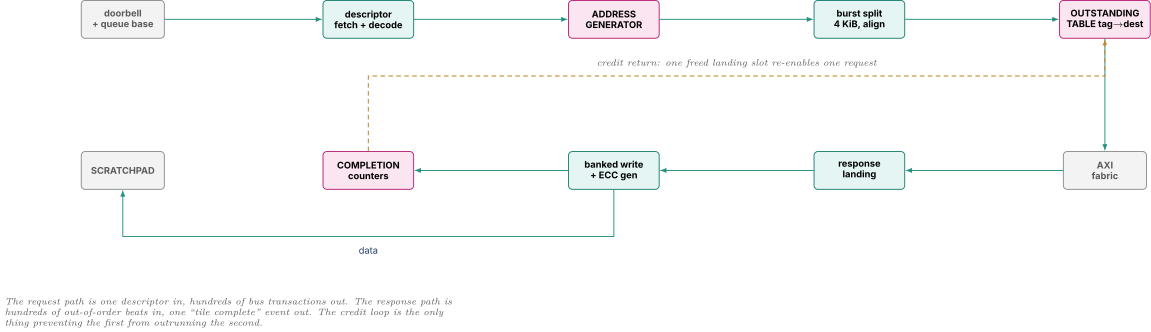
The job is not that. The job is to extract a tile of a multi-dimensional tensor out of a linear address space, deliver it into a banked scratchpad in the layout the array wants, do it far enough ahead that the array never waits, and never exceed the buffering you have. Four distinct hard problems, and they are:
The source is strided, not contiguous. A tile of an image is a rectangle inside a larger rectangle, so it is a set of short runs separated by a stride. Section 8.3.
The latency is enormous relative to the deadline. DRAM round trip is hundreds of nanoseconds while the array consumes a scratchpad line every nanosecond, so the engine has to be running hundreds of requests ahead. Section 8.5.
The responses come back out of order. The memory system reorders freely. Section 8.4.
Nothing may ever be dropped or overrun. There is no retry and no backpressure to the array. Section 8.6.
8.2 Descriptor processing
Software must not write a register per transfer, because at a few microseconds per tile that would consume a core. So work is described in memory, as descriptors, and the engine fetches them itself. SoC Integration and Interfaces section 6.3 covers the ring structure and the ownership-bit ordering hazard in full, and that material is a prerequisite rather than something to repeat. What is specific to an accelerator DMA is what the descriptor contains and what the fetch engine must do with it.
A tensor descriptor is not an address and a length. It is closer to:
| field | purpose |
|---|---|
| source base address | where the tensor starts in the linear address space |
| destination base | where in the scratchpad the tile lands |
| element size | bytes per element, which sets the innermost run length |
| per-dimension count | how many steps in each of typically three or four dimensions |
| per-dimension source stride | how far to jump in the source between steps of that dimension |
| per-dimension destination stride | the same for the scratchpad, which is usually a different layout |
| format and transform | dtype, optional decompression, optional layout transpose |
| next-descriptor pointer | for chaining |
| completion policy | interrupt, event, counter increment, or silence |
Three things the fetch engine must do that are easy to get wrong.
Prefetch the next descriptor while the current one is executing. A descriptor fetch is itself a memory read at full DRAM latency. If the engine fetches descriptor only after finishing descriptor , there is a several-hundred-nanosecond hole in the data stream between every pair of tiles, and at a tile time of a microsecond that is tens of percent of the bandwidth gone. So descriptor fetch is pipelined ahead, typically two or three deep, which immediately raises the question of what happens when software rewrites a descriptor the engine has already fetched. The answer is that the ownership protocol forbids it, and an assertion should check it.
Handle chaining without stalling. Linked descriptors let one doorbell launch a whole layer's worth of transfers. The engine walks the chain and only reports completion at the end, or at descriptors marked for it.
Respect ordering only where ordering is required. Descriptors within a chain are usually independent, so their transactions may interleave freely on the bus, which is what makes full bandwidth achievable. But a completion write must not become visible before the data it reports, which is the same acquire-release problem SoC Integration and Interfaces describes on the software side, and on the hardware side it means the status write is either issued on the same AXI ID as the data or held until the data's write responses have returned.
8.3 Address sequencing and tensor-surface traversal
This is the heart of it. Work an example completely.
Take an activation surface in NHWC layout, which means the channel index varies fastest, then width, then height. Dimensions: height , width , channels , one byte per element. The element at sits at
so the strides are 1 for channels, 64 for width, and 3584 for height.
Now ask for a tile: 8 rows, 8 columns, all 64 channels. That is bytes of useful data. What does the address stream look like?
The innermost 64 bytes, all channels at one , are contiguous. The next step in advances by exactly 64, which is where the previous run ended, so the 8 columns are contiguous too. One row of the tile is a single 512-byte run. The step in advances by 3584, which is a jump. So the tile is 8 runs of 512 contiguous bytes, at a stride of 3584 bytes.
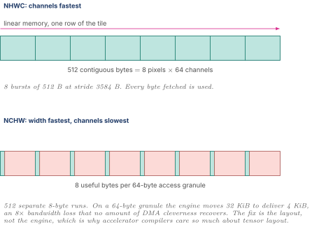
That comparison is the single most useful thing to be able to say about tensor DMA, because it shows the engine and the data layout are one design, not two. The same request, the same tile, the same total useful bytes, and an eightfold difference in delivered bandwidth decided entirely by which index varies fastest.
The address generator in RTL is a nest of counters with an adder per dimension. For a four-dimensional descriptor:
// One step of the traversal. cnt[d] counts within dimension d,
// and addr accumulates the stride of whichever dimension advanced.
always_ff @(posedge clk) begin
  if (step_en) begin
    if (cnt[0] != count[0]-1) begin
      cnt[0] <= cnt[0] + 1;  addr <= addr + stride[0];
    end else if (cnt[1] != count[1]-1) begin
      cnt[0] <= '0;  cnt[1] <= cnt[1] + 1;
      addr <= addr + stride[1] - (count[0]-1)*stride[0];
    end else if (cnt[2] != count[2]-1) begin
      cnt[0] <= '0;  cnt[1] <= '0;  cnt[2] <= cnt[2] + 1;
      addr <= addr + stride[2] - (count[1]-1)*stride[1]
                              - (count[0]-1)*stride[0];
    end else begin
      done <= 1'b1;
    end
  end
end
Two design notes that show experience. The rewind terms, the subtractions, should be precomputed once per descriptor rather than multiplied per step, because a multiplier in the address path is both area and a timing risk. And the priority chain across dimensions is a carry chain. At four dimensions it is trivial, at eight it is a real timing arc and wants a lookahead structure, which is the same argument as the carry-lookahead adder in Arithmetic Hardware wearing different clothes.
Burst formation comes next, and it has hard rules from the protocol. AXI requires that a burst not cross a 4 KiB boundary, so a 512-byte run starting at offset 0xF00 within a 4 KiB page must be split into 256 bytes and 256 bytes. The engine must also respect the maximum burst length, keep bursts aligned to the data-bus width where possible, and avoid emitting narrow transfers when a wider one would do. Getting this wrong does not produce a functional failure. It produces a design that passes every test and delivers 60 percent of its target bandwidth, which is worse, because it is found late.
Address translation deserves a sentence because these roles name it. If the engine issues virtual addresses it must go through an IOMMU or system MMU, which means a translation lookaside buffer inside or in front of the engine, translation misses that take a page-table walk of several hundred nanoseconds, and the possibility that a tile spans a page boundary and therefore two translations. Virtual Memory and Memory Ordering and I/O Architecture cover the mechanism. The accelerator-specific consequence is that a tile whose physical pages are scattered breaks the contiguity assumption of 8.3, so large pages are not a nicety, they are a bandwidth feature.
8.4 Out-of-order responses
AXI permits read data to return out of order across different transaction IDs, and memory systems exploit that heavily. A request that hits an open DRAM row returns long before one that needs a row activation, and the controller reorders deliberately to maximise row-buffer hits, as DRAM and Memory Controllers describes. So the engine must assume responses arrive in an arbitrary order.
There are two ways to cope and the choice matters.
Reorder them. Allocate a buffer, hold early responses until their predecessors arrive, and present the stream in order. This is what a CPU load path does, and it costs a buffer sized for the worst-case reordering window plus the latency added by waiting.
Do not reorder them. Carry the destination with the request. When a transaction is issued, its tag indexes an entry in the outstanding table holding the scratchpad address it belongs to and its byte count. When the response arrives, look up the tag, write the data to that address, and increment a completion counter for the owning descriptor. Order never mattered because the scratchpad is addressable and nothing downstream reads it until the whole tile is present.
For an accelerator DMA writing into a scratchpad, the second is strictly better, and being able to say why is the point of the question. The consumer is not a stream, it is a memory region, and the only thing the array cares about is that the region is complete before it reads. So the correct completion mechanism is a counter compared against the descriptor's expected transaction count, not an in-order pointer.
The exceptions are real and worth naming, because an interviewer will look for whether you know the second design is not universal. Order matters when the destination is genuinely a stream, such as a FIFO feeding the array edge directly with no scratchpad in between. It matters when the payload is compressed, because decompression is inherently sequential, so a compressed tile must be reassembled in order before it can be expanded, and the mention of compression is exactly this problem. And it matters when the destination is another agent's memory with ordering requirements of its own.
Tag capacity is worth a note. If the fabric supports only 16 AXI IDs but you need 240 outstanding reads, that is not a contradiction. Multiple transactions may share an ID, and within an ID they return in order. So the outstanding table becomes a set of per-ID queues rather than a flat array, which costs a little control complexity and buys you the transaction count you need without demanding a wide ID field from the fabric.
8.5 Buffer sizing, which is Little's law and nothing else
The question "how deep should the outstanding-transaction tracking be" has an exact answer, and it is the same answer as the credit sizing in Interconnect and AMBA.
Get to it by counting one request first, before any formula. Issue a single 64-byte read and wait for it. If the DRAM round trip is 300 ns, that one request delivers 64 bytes every 300 ns, which is MB/s. That is the entire bandwidth a strictly one-at-a-time engine can achieve, no matter how wide the bus is, because the bus is idle for all but a sliver of those 300 ns. To reach Model Machine M's 51.2 GB/s you need such requests all in the air simultaneously. Nothing about that reasoning needed a theorem.
The theorem is just the general form of it. To sustain throughput over a round-trip latency , the amount of data that must be in flight at all times is
This is Little's law, and it is not an approximation. If less than that is outstanding, the data channel goes idle waiting for responses and throughput falls short in exact proportion.
Work it for Model Machine M. Target 51.2 GB/s, DRAM round trip 300 ns.
Convert to transactions. With 64-byte reads that is 240 outstanding. With 256-byte reads it is 60. That is a strong argument for larger bursts on its own. The tracking structure shrinks by the same factor. At 240 entries with, say, 40 bits of state each (scratchpad address, byte count, descriptor id, valid), the table is about 9,600 flops, which is meaningful area and a CAM-like lookup if it is searched rather than indexed. Making it a directly indexed array rather than a CAM, by using the AXI ID as the index, is the standard trick and it is why the tag-carries-destination scheme of 8.4 is worth the design effort.
Then check the other end. Fifteen kilobytes in flight means fifteen kilobytes of landing space must exist somewhere, either as a dedicated buffer or as reserved scratchpad. On a 256 KiB scratchpad that is 6 percent, which is acceptable. If the latency were instead of 300 ns, it would be 51 KiB, which is 20 percent, and the conversation changes.
Three further sizing rules that fall out of the same arithmetic and are worth having ready.
Double buffering needs the tile time to exceed the fill time, which section 4.3 already checked. It found of compute against of load, so the prefetch depth of one tile pair is sufficient. If it were the other way round, one extra buffer would not save you, because the deficit is per tile and compounds.
The descriptor prefetch depth is the same calculation at a different scale. If a descriptor fetch takes 300 ns and a descriptor's worth of work takes , one descriptor of lookahead suffices with margin. If descriptors are small, you need more.
Latency, not bandwidth, is what you are buying with all of this. Every one of these buffers exists to convert a latency problem into an area problem, and stating it that way is a good way to show you understand the shape of the design rather than the formula.
8.6 Back-pressure, and the rule that prevents deadlock
Three places can stall.
The fabric can stall the read-address channel, which is fine and normal.
The scratchpad write port can be busy, because the compute array is reading the same memory. The DMA and the array contend for banks, so there is an arbiter, and it is a real arbiter with a real fairness question, exactly the material in Arbiters FIFOs and CAMs. Starving the DMA stalls the next tile. Starving the array stalls this tile. The usual resolution is to give the array strict priority and to bank the scratchpad so the conflict is rare rather than arbitrated often.
The consumer may not have freed the buffer the tile is going into, because the array has not finished with the previous contents.
Now the rule that makes all three safe, and it is one sentence.
Never issue a read whose landing space has not already been reserved.
If you issue anyway and the response arrives with nowhere to go, you have exactly two options and both are bad. Buffer it, which means you needed the buffer after all and sized it wrong. Or stall the AXI read-data channel by de-asserting RREADY, which blocks a shared channel and stalls every other master behind you. On a shared fabric that is not a local performance problem, it is a system-wide one, and if the agent you are blocking is one you are indirectly waiting on, it is a deadlock, of exactly the circular-dependency shape Verification Methodology describes as the classic multi-queue formal target.
Implement the rule as credits. One credit equals one reserved landing slot of a fixed size. The issue logic decrements on request and the completion path returns the credit when the data has been written and the slot re-freed. Size the credit count at the Little's-law number from 8.5, round up, and now the buffer can never overflow by construction rather than by argument. This is the same credit-based flow control as the fabric's own, applied one level down, and the reason to prefer it over a ready/valid stall is precisely that it moves the stall from a shared resource to a private one.
8.7 What breaks, which is the list worth memorising
The array reads a tile before the DMA finished writing it. The single most common accelerator bug. There is no coherence, no valid bit, and no miss. The array reads stale bytes and produces plausible wrong numbers. It is a race between two engines, so it is timing-dependent, workload-dependent, and often only appears when a DRAM refresh lands in the wrong place. The fix is a completion counter the control FSM waits on, and the verification hook is an assertion that fires if a scratchpad region is read while its outstanding-write count is non-zero. Write that assertion on day one.
Descriptor rewritten under the engine. Software updates a descriptor the prefetcher already consumed. Prevented by the ownership protocol, caught by an assertion on the ownership bit at fetch time.
The completion write passes the data. Software sees "done" and reads a buffer that is still filling. Discussed in 8.2 and in SoC Integration and Interfaces 6.3.
A tile spans a page boundary and the second page is not mapped. The transfer faults halfway, leaving the scratchpad partially written, and the recovery story has to exist rather than being discovered in the lab.
Bandwidth silently 60 percent of target because of unaligned bursts, 4 KiB splits, or a layout that produced 8-byte runs. Functionally perfect, commercially unacceptable, and found only by a performance test that somebody has to have written.
The credit accounting leaks. One credit not returned on an error path, and after a few hours of running the engine has zero credits and stops forever. This is a good formal target. The sum of issued and returned credits is an invariant, and it is a small enough property to prove rather than simulate.
8.8 Power, which is where an unusual amount of leverage lives
A DMA engine is idle a lot. Between descriptors, between layers, and whenever the array is compute-bound, most of its structures have nothing to do. That makes it an unusually good target for everything in Power Fundamentals and Clock Gating, and it is worth saying so in an interview for a role that names low power explicitly.
The address generator, the burst splitter, and the descriptor decoder are all idle whenever no descriptor is active, and their idle condition is architecturally obvious rather than inferred, which is the coarse-grained gating case. The outstanding table is a wide register array whose entries change only on issue and completion, so it is a textbook fine-grained gating target with a high-value enable. The response datapath toggles on every beat and should be operand-isolated so that a beat destined for one bank does not toggle the write path of the others. And a whole DMA channel that is unused in a given network layer is a power-gating candidate, with the break-even arithmetic from that note deciding whether the idle window is long enough to justify it.
09.Part 9, what "mapping an algorithm onto hardware" means as an RTL deliverable
The phrase appears in accelerator job role descriptions constantly and it is vague enough that candidates answer it vaguely. It is not vague. It has a concrete output, and this part is that output.
9.1 The chain, from a layer to a netlist
Suppose the requirement is to run a bf16 GEMM on Model Machine M at better than 90 percent of peak. Here is what "mapping" produces, in order, and each step is a document or a file that somebody reviews.
One. The loop nest and the transformation applied to it. Write the original three loops. Then write the tiled and reordered version with the tile factor as a symbol. This is the artefact that a compiler person and a hardware person can both read, and it is the contract between them.
Two. The tile size, with the arithmetic that justifies it. Section 4.3 gives it. , ridge point 40, so . The nearest power of two is 128. Capacity is KiB and the scratchpad is 256 KiB, so it fits. Three numbers and a comparison. If the specification says without those three numbers, the specification is incomplete, and reviewers should say so.
Three. The dataflow choice, with the shape argument. is long and the batch dimension is unremarkable, so output-stationary, per Part 3. Say what would change the answer.
Four. The array RTL. A parameterised two-dimensional generate of the MAC cell from 2.2, with the pipeline depth of the multiplier and adder stated, the accumulator width justified per 5.5, and the rounding and saturation policy written down rather than inherited from whatever the multiplier IP happened to do.
Five. The scratchpad banking calculation. The array consumes 32 bf16 values and 32 bf16 values per cycle, so 64 bytes per operand port per cycle. An SRAM macro of the kind SRAM Arrays and ECC describes gives one 256-bit access per cycle, which is 32 bytes, so each operand port needs at least two banks and realistically four to allow the DMA to write while the array reads. Then the address swizzle. The bank index must be chosen so the array's natural access stride never lands two simultaneous reads in the same bank. That is a small piece of combinational logic that is easy to get subtly wrong and easy to prove correct formally, since it is a statement about a function of address bits.
Six. The address generators and the descriptor format. Part 8.
Seven. The control FSM. Sequences load, compute, and store with double buffering, issues the skew, waits on completion counters, and handles the ragged edge when the matrix dimension is not a multiple of . The ragged edge is where the bugs are, and the ragged edge is where interviewers go.
Eight. The power intent. Per-column and per-row clock gating when the active tile is narrower than the array, operand isolation on the multipliers when a PE has no valid data, and the coarse gate on the whole array between layers. Power Fundamentals and Clock Gating is the method. The accelerator-specific observation is that the enable conditions here are architecturally known rather than inferred, because the control FSM knows exactly which PEs are active in the ragged edge, so the gating opportunity is unusually large and unusually easy to prove correct.
Nine. The assertions. Named in the Apple DMA role description explicitly, as "high quality RTL with embedded assertions and cover points." The list for this design: no accumulator overflow for the architectural maximum , no scratchpad read of a region with a non-zero outstanding-write count, the credit sum invariant from 8.7, one-hot control encodings, no bank conflict on the array's read ports, back-pressure never causes a dropped beat, and cover points on the ragged-edge tile shapes, because those are the cases random stimulus under-weights.
Ten. The correlation against a performance model. Somebody has a C++ or Python model that predicted 92 percent of peak. The RTL delivers some number. When they disagree, one of them is wrong and finding out which is a week of work. This is where Performance Modeling applies directly and it is the step most likely to be skipped and most likely to be regretted.
Eleven. PPA closure. The array's regularity is its physical selling point: identical cells, nearest-neighbour wires, one timing arc replicated, a floorplan you tile. Whether that promise survives contact with the skew registers, the edge feeds, and the accumulator drain path is a real question for STA Synthesis and Physical Design.
9.2 The thing that makes it hard
The eleven steps above look sequential and are not. Change the tile size in step two and the banking in step five changes, the descriptor strides in step six change, the FSM's ragged-edge handling in step seven changes, and the floorplan in step eleven may stop closing. Change the dataflow in step three and the accumulator width, the drain path, and the assertion list all move.
So the honest description of the job is that mapping is a search over a space where the constraints are coupled, and the deliverable is not just the chosen point but the written argument for why that point and not its neighbours. An interviewer asking "how would you map this layer" is usually checking whether you know the space is coupled, and the strongest possible answer starts by asking what the machine's ridge point is, because that one number prunes most of the space immediately.
10.Part 11, interview questions with model answers
Eighteen questions, written the way a strong candidate would actually speak them rather than the way a textbook would state them. Each has the follow-up the interviewer reaches for next, and where the question is a trap, the trap is named.
11.1 Why does matrix multiply need special hardware at all?
Answer. It is not the arithmetic. An by multiply is multiply-accumulates, and a modern CPU can do a lot of those. The problem is the ratio of arithmetic to memory traffic. If you implement the three loops literally, every MAC fetches two fresh operands, so you get half a MAC per operand fetched, which means the arithmetic intensity is about regardless of matrix size, half a FLOP per byte in bf16. That number is fixed, and it is far below the balance point of any real machine, so you sit on the bandwidth roof no matter how much compute you build.
What makes the operation special is that it can be much better. Each element of participates in different outputs, so the ideal traffic is elements for FLOPs, giving intensity , which grows linearly with size. So matrix multiply is the rare kernel where reuse is available if you build the machine that captures it. Special hardware exists to capture that reuse. Everything else, the systolic array, the scratchpad, the tiling, the DMA, is machinery for turning the naive number into the ideal number.
Follow-up. So why not just add a big cache to a CPU? Because a cache captures reuse only if the access order happens to have locality, and getting the order right is the tiling transformation, which the compiler must do anyway. Once you have done the tiling, the cache's prediction machinery, tags, replacement, and miss handling, is pure overhead you are paying for something you already know. And the CPU still cannot deliver 2048 operands per cycle from a register file, which is the actual constraint.
11.2 Define arithmetic intensity and compute it for a GEMM. What raises it?
Answer. FLOPs performed divided by bytes moved between the compute and the next level of memory. For an cubed GEMM with perfect reuse it is over , which simplifies to . For 256 by 256 matrices in bf16 that is about 85 FLOPs per byte.
Three things raise it. Larger tiles, and this is the dominant one, because for a blocked GEMM the intensity is approximately the tile dimension divided by the bytes per element, so intensity is set by tile size and nothing else. Narrower data types, because halving the bytes doubles the intensity for free. And batching, in the matrix-vector case, because it converts a shape with no reuse into one with reuse.
The number only means something against the machine's ridge point, which is peak FLOP/s divided by bandwidth. If the machine's ridge is 40 and your kernel is at 85, you are compute-bound and should stop optimising memory. If your kernel is at 12, you are running at 30 percent of peak and no amount of extra MACs will help.
Follow-up. What is the ridge point of a machine you have used? If you do not know, say so and derive one from published numbers instead. A part with 400 TFLOP/s and 3 TB/s has a ridge near 133 FLOPs per byte, which is a useful thing to have in your head because it tells you immediately that any matrix-vector operation on that part is hopeless.
Trap. Quoting intensity without saying which memory level it is measured against. Intensity against DRAM and intensity against the on-chip scratchpad are different numbers for the same kernel, and the systolic array exists precisely to make the second one large.
11.3 Why a systolic array instead of 1024 independent MAC units behind a crossbar?
Answer. Operand bandwidth and wire length, in that order.
A thousand independent MACs need two thousand operands per cycle. At 1 GHz in bf16 that is four terabytes a second out of the on-chip memory, which needs on the order of 128 to 256 conflict-free banks and a 2048-endpoint crossbar. The crossbar would be bigger and hotter than the multipliers, and its wires, not the arithmetic, would set the clock period.
The systolic array replaces almost all of that with nearest-neighbour connections. Each cell takes what its neighbour had last cycle and passes it on, so in steady state only operands cross the array boundary per cycle while MACs happen inside. For a 32 by 32 array that is 64 operands instead of 2048, a factor of 32. The one-line version is that a systolic array converts register-file read ports into short wires, and short wires are the cheapest resource on a chip.
There is a physical-design argument on top. Every wire is one cell pitch long, every timing arc is the same arc replicated, and the floorplan is one cell tiled, so it closes timing at a frequency a crossbar-based design would not reach.
Follow-up. What does that cost you? Flexibility and utilisation. The array natively computes an by tile, so a 16 by 16 layer on a 256 by 256 array uses 0.4 percent of it, and the fill and drain of cycles is dead time unless consecutive tiles are overlapped. That is why the industry has drifted toward many small arrays rather than one huge one.
11.4 Compare output-stationary, weight-stationary, and row-stationary.
Answer. They are choices about which loop of the matrix-multiply nest runs inside a single PE. does not depend on , does not depend on , and does not depend on , so whichever loop you run inside the cell, one operand sits still in a register and is read for free.
Output-stationary runs the loop in the cell, so the partial sum never moves until the end. It minimises partial-sum traffic, which matters disproportionately because the accumulator is the widest thing in the datapath, four bytes against one for int8. It pays by requiring both inputs to arrive every single cycle. It wins when the reduction dimension is long.
Weight-stationary runs the loop in the cell, so a weight is loaded once and reused across every row of activations. It minimises weight fetch. It pays by moving partial sums down the columns every cycle, and those are the wide operand. It wins when the batch dimension is long, which is why it dominated the first generation of datacenter inference chips, and the published TPU v1 description is the canonical example.
Row-stationary, from Eyeriss, is a different kind of answer. It maps a one-dimensional convolution into each PE so that filter weights, input activations, and partial sums all get reuse locally, and it optimises total data-movement energy rather than any single operand's traffic. It matters because the published energy numbers put a DRAM access at roughly 200 times a MAC and a local register file access at about 1, so total accesses in the cheap places beats fewer accesses in the expensive ones. It pays in mapping and control complexity, and it is shaped for convolution, so it does less for transformer GEMMs.
The rule I would state is that each dataflow amortises a fixed cost over the loop it runs inside the PE, so you pick by asking which loop bound is largest in the layers you care about.
Follow-up. Which for LLM token generation? Neither of the first two works well, and saying that is the right answer. Decode is a matrix-vector product, so the batch dimension is one, which destroys weight-stationary's amortisation completely. One MAC per weight fetched, zero reuse. Output-stationary at least keeps the reduction, but the array is one row wide, so utilisation collapses. The real answer is that you fix it above the dataflow layer by batching many requests together, which manufactures the missing dimension.
Trap. Answering as if one dataflow is correct. Real designs are hybrids, usually output-stationary inside the PE with a weight-stationary outer loop, and saying that the taxonomy is a reasoning tool rather than a menu is a stronger answer than picking one.
11.5 How do you choose the tile size for a blocked GEMM?
Answer. Two calculations that meet in the middle.
From the roofline side, the arithmetic intensity of a blocked GEMM is approximately the tile dimension divided by the bytes per element. So if the machine's ridge point is 40 FLOPs per byte and I am in bf16 at two bytes, I need a tile of at least 80 to be compute-bound.
From the capacity side, I need an tile, a tile, and a tile resident, and I need the input tiles double-buffered so the DMA for the next step overlaps the compute on this one. With two-byte inputs and a four-byte accumulator that is plus plus , so 12 bytes. At equals 128 that is 192 kilobytes.
So on a machine with a 256 kilobyte scratchpad, equals 128 is the answer. It is above the roofline threshold of 80, and it fits with room to spare. And the argument runs backwards just as well, which is the version that matters when you are specifying the chip rather than programming it. If the roofline says I need a tile of 80 and the natural power of two is 128, then the scratchpad has to be at least 192 kilobytes, and that is where the SRAM budget number comes from.
I would then check it a third way, in time. At equals 128 the load takes 1.28 microseconds and the compute takes 2.05, so the DMA hides completely, and the ratio 0.625 is exactly the ridge point over the arithmetic intensity. If those three routes disagree, one of my models is wrong.
Follow-up. What if the matrix dimension is not a multiple of the tile? You get a ragged edge, and the ragged edge is where the bugs and the lost performance both live. The control has to handle partial tiles, the array runs under-utilised on them, and the address generator has to produce a shorter run. I would put explicit cover points on ragged tile shapes because random stimulus under-weights them.
11.6 Why does bf16 exist when fp16 already existed?
Answer. Dynamic range, and it is worth being precise that bf16 is less accurate than fp16, not more.
fp16 has five exponent bits and ten mantissa bits. bf16 has eight and seven. So bf16 has three fewer significand bits, about 0.4 percent relative error against fp16's 0.05 percent, and three more exponent bits, giving it the same range as fp32.
The reason that trade is correct for neural networks is that training values span an enormous range. A gradient of is completely ordinary after a few dozen layers of chain rule. In fp16 the smallest normal value is and even the smallest subnormal is about , so flushes to exactly zero. The gradient does not get imprecise, it disappears, and the weight it was going to update never updates, silently. At the other end, a sum of squares around overflows fp16 to infinity and then the first subtraction produces a NaN. In bf16 the range is and neither happens.
The imprecision, meanwhile, does not hurt, because stochastic gradient descent is already a noisy process and the next mini-batch corrects a 0.4 percent error. Networks turn out to be robust to precision and fragile to range.
There are two hardware bonuses. bf16 is just fp32 with the low 16 bits removed, same exponent width and same bias, so conversion is a truncate or a zero-pad with no range check, which means the converter is a wire. And the significand multiplier is 8 by 8 instead of 11 by 11, so the partial-product array is about half the size of fp16's and roughly a ninth of fp32's, which is why at fixed area you get many more of them.
Follow-up. Why not just use fp32 everywhere? Because the multiplier area goes as roughly the square of the significand width, so fp32 costs about nine times the array area of bf16 for arithmetic the workload does not need, and it doubles every byte of weight traffic in a workload that is usually bandwidth-bound.
Follow-up. What did people do before bf16? Loss scaling. Multiply the loss by a large constant so gradients shift into fp16's band, then scale the updates back down, with a dynamic controller that detects overflow, backs off, and retries. It works and it is software complexity in the innermost loop of training, which is exactly what bf16 removed.
Trap. Saying bf16 is "more precise" or "better." It is less precise and it is better for this workload, and the distinction is the whole answer.
11.7 You have an int8 MAC array. How wide is the accumulator, and why?
Answer. int32, and the arithmetic is short. The largest int8 product is 127 times 127, which is 16,129, needing 15 bits. Summing of them needs about plus a sign bit. At equals 1024 that is 25 bits. int32 has room for about 133,000 accumulations, so it cannot overflow for any real layer, which is why it is the universal choice.
I would add that int32 is overkill and that is a legitimate PPA conversation. If the architecture bounds at 1024, 25 bits carries every representable sum and 26 gives a guard bit, so against int32 that saves six bits of flop and six bits of adder per cell, which across a thousand PEs is a real area line item. The right answer is usually to size for the architectural maximum and to write that maximum into the specification, because the failure mode of getting it wrong is silent wraparound producing plausible wrong numbers.
Follow-up. What if the inputs are bf16? Then you accumulate in fp32, and the reason is more interesting than the integer case. bf16 has eight significand bits, so once the running sum is 256 times the addend, adding the addend rounds to no change. Accumulate a thousand values of 1.0 in bf16 and the sum sticks at 256 forever, an error of 75 percent with no exception raised. fp32 has 24 significand bits, so stagnation does not happen until about 16 million. The general rule is that you multiply in the narrow format because a partial-product array grows as the square of its operand width, and you accumulate wide because a register and an adder grow only linearly, so you are trading a quadratic cost for a linear one in the direction that makes the quadratic one small.
Trap. Saying "int32 because that is what everyone uses." The interviewer wants the overflow arithmetic, and it takes ten seconds to do.
11.8 Explain per-tensor versus per-channel quantisation, and what changes in the hardware.
Answer. Quantisation maps reals to int8 with a scale, so a real value is the integer times the scale. Per-tensor gives the whole weight tensor one scale, set by the largest magnitude anywhere in it. Per-channel gives each output channel its own.
The reason per-channel exists is a concrete failure. Suppose one output channel's weights span plus or minus 0.9 and another's span plus or minus 0.007. With one scale of 0.9 over 127, the second channel's largest weight quantises to 1, so that entire filter becomes ternary, minus one, zero, and plus one. You have lost about seven bits on that channel, and the accuracy drop shows up as a mysterious couple of percent that nobody can localise. Per-channel gives that channel its own scale and it uses the full range.
In hardware, three things must exist. An int32 accumulator. A requantisation stage that scales the accumulator back to int8, which is not a divide but a precomputed fixed-point multiply and a rounding right shift, plus a zero-point add and a saturate. And for per-channel, a small scale table indexed by output channel, holding a multiplier and a shift per channel, loaded when the weights are loaded and read by the requantisation stage.
Follow-up, and this is the real question. Could you do per-channel along the input axis instead? No, and the reason is exact. The integer array works because the scales factor out of the sum. The sum of times equals times the sum of , so the array does pure integer MACs and one scale multiply happens at the end. That factoring requires the scale to be constant with respect to the reduction index. Per-output-channel indexes by the output column, which is outside the sum, so it is free. Per-input-channel would index by , which is inside the sum, so every MAC would need its own floating-point scale multiply on the critical path and the integer array is destroyed. The rule is that you may quantise per-channel along any axis except the reduction axis.
Follow-up. What about block quantisation? That deliberately puts a shared scale inside the reduction, over a block of 32 or 64 elements, and the hardware handles it by accumulating a block in integer, applying that block's scale, and adding into a wider running accumulator. It costs a scale-apply stage every 32 accumulations, which is why block sizes are 32 and not 4.
11.9 Why is large-language-model token generation memory-bandwidth-bound? Give me numbers.
Answer. Because generation produces one token at a time, so every matrix multiply has exactly one row, and a one-row matrix multiply has no reuse by construction. You read a weight and you use it once.
Take a seven-billion-parameter model in fp16. One decode step does about FLOPs, which is 14 gigaFLOPs, plus about a gigaFLOP of attention over the cache. To do that it must read all 14 gigabytes of weights, plus the KV cache, which at 32 layers, 4096 hidden and a 2048-token context is another gigabyte. So roughly 15 gigaFLOPs against 15 gigabytes, giving an arithmetic intensity of about one FLOP per byte.
For comparison, prefill on a 2048-token prompt does 28.7 teraFLOPs against the same 14 gigabytes of weights, so its intensity is about 2000. Same model, same silicon, three orders of magnitude apart.
Turn it into time. On a machine with a terabyte per second of bandwidth, 15 gigabytes takes 15 milliseconds, so 67 tokens per second is a hard floor set by bandwidth alone. If that machine also has 400 teraFLOP/s of compute, the arithmetic takes 37 microseconds. The matrix engine is busy for a quarter of one percent of the time.
Follow-up. How would you make it faster? Not with more MACs, which is the trap in the question. Batching is the primary lever, because serving requests concurrently reads the weights once and uses them times, so the intensity becomes roughly , and to hit a ridge point of 400 you need a batch near 400. That is why continuous batching was such a large practical win. The ceiling on batching is the KV cache, which is per-request and therefore does not amortise, which is exactly why grouped-query attention and KV-cache quantisation matter. The other levers are all about reading fewer bytes: weight quantisation to int8 or fp8, sparsity if the hardware can skip, and speculative decoding, which uses a small model to propose several tokens and verifies them in one pass of the big model, converting several memory-bound steps into one step with several rows.
Follow-up. What does that imply for the chip? That prefill and decode want different machines. Prefill wants a big array and modest bandwidth, decode wants enormous bandwidth and barely uses the array. One chip that does both well is overprovisioned somewhere, which is why disaggregated serving, running prefill and decode on separate machines, exists.
11.10 Design the DMA that feeds this array. What is in the descriptor?
Answer. The key point is that it is not a memcpy engine, because the source is a tile of a multi-dimensional tensor sitting inside a linear address space, so it is a set of strided runs rather than a contiguous range.
The descriptor therefore carries a source base address, a destination address in the scratchpad, an element size, and then for each of three or four dimensions a count and a source stride and a destination stride, because the scratchpad layout is usually not the DRAM layout. Plus a data type and any transform such as decompression, a next-descriptor pointer for chaining, and a completion policy.
The engine has an address generator that is a nest of counters, one adder per dimension, where the stride to add is the one belonging to whichever dimension advanced. I would precompute the rewind terms, the count-minus-one times stride subtractions, once per descriptor rather than multiplying per step, because a multiplier in the address path is area and a timing risk.
Downstream of the address generator is burst formation, which has to respect the 4-kilobyte boundary rule, the maximum burst length, and alignment, and that stage is where designs quietly lose 40 percent of their bandwidth without failing any functional test.
Follow-up. Work an example. Take an NHWC activation surface, 56 by 56 by 64 channels at one byte. Strides are 1 for channel, 64 for width, 3584 for height. An 8 by 8 by 64 tile is 4096 bytes, and because channels are contiguous and the width stride is exactly 64, a whole tile row of 8 pixels is 512 contiguous bytes. So the tile is eight bursts of 512 bytes at a stride of 3584, which is efficient.
Now the same tile in NCHW. Width is fastest and channels slowest, so a run is 8 bytes and the tile is 512 separate 8-byte runs. On a memory system with a 64-byte access granule you fetch 32 kilobytes to deliver 4, an eightfold loss. The point is that the DMA and the tensor layout are one design, not two, and no amount of cleverness in the engine recovers a bad layout.
Follow-up. What about virtual addresses? Then it goes through an IOMMU, so there is a TLB in or in front of the engine, translation misses cost a page-table walk, and a tile can span two translations. The accelerator-specific consequence is that scattered physical pages break the contiguity assumption, so large pages are a bandwidth feature rather than a nicety.
11.11 Your DMA gets read responses out of order. How do you handle it?
Answer. By not caring, if the design is right.
AXI lets read data return out of order across IDs, and memory controllers reorder deliberately to maximise DRAM row-buffer hits, so out-of-order is the normal case rather than an exception. The wrong answer is to build a reorder buffer that restores order, because that costs a buffer sized for the worst-case reordering window and adds latency for no benefit.
The right answer for a DMA writing into a scratchpad is to carry the destination with the request. When a transaction is issued, its tag indexes an outstanding-transaction table entry holding the scratchpad address it belongs to, its byte count, and the descriptor that owns it. When the response comes back, look up the tag, write the data at that address, and increment a completion counter. Arrival order never mattered, because the destination is an addressable memory and nothing reads it until the whole tile is present. The completion condition is a counter reaching the expected transaction count, not a pointer reaching the end.
Follow-up. When would you actually need a reorder buffer? Three cases. When the destination is genuinely a stream, such as a FIFO feeding the array edge with no scratchpad in between. When the payload is compressed, because decompression is sequential, so the tile has to be reassembled in order before it can be expanded. And when the destination is another agent with ordering requirements of its own.
Follow-up. What if the fabric only gives you 16 IDs and you need 240 outstanding reads? Not a contradiction. Multiple transactions can share an ID and within an ID they return in order, so the tracking becomes a small set of per-ID queues rather than a flat table. That is a little more control logic in exchange for not demanding a wide ID field from the fabric.
11.12 How many outstanding reads should the engine support?
Answer. Little's law, and it is exact rather than a heuristic. To sustain a throughput over a round-trip latency , you must keep bytes in flight at all times. Below that the data channel goes idle waiting and throughput falls short in exact proportion.
For a target of 51.2 gigabytes a second and a 300-nanosecond DRAM round trip, that is 15,360 bytes, about 15 kilobytes. With 64-byte reads that is 240 outstanding transactions. With 256-byte reads it is 60.
That factor of four is itself an argument for larger bursts, because the tracking structure shrinks by the same factor. At 240 entries of roughly 40 bits each the table is about 9,600 flops, which is real area, and it wants to be a directly indexed array rather than a CAM, which is another reason to index it by the transaction tag.
Then I would check the other end, where 15 kilobytes in flight means 15 kilobytes of landing space must exist. On a 256-kilobyte scratchpad that is 6 percent, acceptable. If the latency were a microsecond it would be 51 kilobytes, 20 percent, and the conversation changes.
Follow-up. What happens if you undersize it? You get a design that is functionally perfect and delivers, say, 60 percent of target bandwidth, and because nothing fails, it is found late. That is why I would want a directed performance test that measures sustained bandwidth against the Little's law prediction, not just a functional regression.
Follow-up. And if you oversize it? Area and power for nothing, plus a longer queue that increases worst-case latency. The throughput-versus-depth curve is linear below the bandwidth-latency product and flat above it, so there is a knee and going past it buys nothing.
11.13 How do you apply back-pressure without deadlocking the fabric?
Answer. There is one rule. Never issue a read whose landing space is not already reserved.
If you issue anyway and the data arrives with nowhere to go, you have two options and both are bad. Buffer it, which means you needed the buffer and sized it wrong. Or stall the read-data channel by dropping ready, which blocks a shared channel and stalls every other master behind you. That is not a local performance problem, it is a system-wide one, and if the agent you are blocking is one you indirectly depend on, it is a deadlock from a circular dependency where every block is individually correct.
So I would implement it as credits. One credit is one reserved landing slot. Issue decrements, and the credit returns when the data has been written and the slot freed. Size the credit count from the Little's law number. Now overflow is impossible by construction rather than by argument, and the stall has been moved from a shared resource to a private one.
Follow-up. What else can back-pressure you? The scratchpad write port, because the compute array is reading the same memory. That is a genuine arbitration problem with a fairness question. Starving the DMA stalls the next tile, starving the array stalls this one. The usual answer is strict priority to the array plus enough banking that the conflict is rare, and I would want a counter on conflict events so the assumption is measured rather than assumed.
Follow-up. How would you verify the credit scheme? Formally. The invariant is that issued credits plus returned credits equals the total, and that the count never exceeds the buffer capacity. It is small-state and intricate, which is the formal sweet spot, and the failure it prevents, a single credit leaked on an error path that stops the engine after four hours, is exactly the kind of thing simulation is bad at finding.
11.14 Your array is 128 by 128 and the layer is 16 by 16. What happens?
Answer. Two hundred and fifty-six of the 16,384 PEs do work, so utilisation is 1.6 percent, and the fill and drain of equals 254 cycles now dwarfs the useful work. It is a disaster, and it is the most important practical limitation of large systolic arrays.
There are several responses and they trade differently. Partition the array into independent sub-arrays that can work on different tiles or different layers concurrently, which is essentially the argument for a grid of smaller engines rather than one big one, and it is visible in published designs such as Meta's 8-by-8 grid of processing elements. Fold the reduction, mapping the small spatial dimension onto the array's other axis so the unused PEs take different ranges and the results are summed afterwards, which needs an extra reduction network. Batch, running several instances of the small layer at once, which works if the workload has them. Or accept it and clock-gate the idle PEs, which does not recover performance but does recover power, and knowing that gating is the fallback rather than the fix is the right framing.
Follow-up. How do you decide array size at architecture time? By profiling the layer shapes of the networks you actually intend to run and looking at the distribution, not the mean. If the shapes span two orders of magnitude, one array sized for the largest is the wrong answer, and the design should either be partitionable or should be several smaller arrays.
Trap. Answering only "it is inefficient." The interviewer wants the number and at least two mitigations.
11.15 How would you clock gate this accelerator?
Answer. This is where an accelerator is unusually easy compared with a CPU, because the idle conditions are architecturally known rather than inferred by synthesis. The control FSM knows exactly which rows and columns of the array are active on a ragged tile, so the enable is a real signal already sitting in the control, not something a tool has to prove.
Four layers of it. Coarse, at the block level, gating the whole array between layers and gating a whole DMA channel that a given layer does not use, driven by the sequencer. Per-row and per-column, gating the PEs outside the active tile shape, which on a ragged edge or a small layer is most of the array. Fine, per PE, gating the accumulator register when no valid operand arrives that cycle, which synthesis will insert automatically if the RTL writes it as a conditional assignment. And operand isolation on the multiplier inputs, which is a big win here because a bf16 multiplier is a large toggling structure and holding its inputs constant when the result will be discarded keeps the whole partial-product array quiet.
I would also be careful about what must not be gated: the descriptor engine's wake path, anything in a synchroniser, and the completion counters, for the reasons in the general clock-gating material.
Follow-up. How much would that save? I would not quote a percentage without measuring it, and I would say so. What I would quote is the method. Run a gate-level power analysis with switching activity from a real network's trace, sort ungated instances by clock power, and work the list. On my previous work that process took a block to 95 percent dynamic gating coverage, and the honest framing there is that coverage is not savings, because savings is coverage times the fraction of cycles the enables are actually low.
Follow-up. What does the gating cost? The gating cell sits on the clock path, so it adds insertion delay that clock-tree synthesis has to balance, and each cell burns its own clock power whether or not it gates anything, which sets a minimum group size for it to pay for itself. On an array of identical PEs the group sizes are large and the enables are architecturally derived, so the economics are unusually favourable.
11.16 How would you verify a systolic array?
Answer. Split it, because the datapath and the control fail differently.
The datapath is wide and its state is essentially all reachable, which is exactly where formal dies. So it gets a reference model and constrained-random stimulus. That means a bit-accurate software model of the array, written from the specification rather than from the RTL, with a scoreboard comparing per-tile results. The important detail is the reference model must implement the same rounding, saturation, and accumulation order as the hardware, because a floating-point accumulation is not associative and a model that sums in a different order will mismatch in the last bits and waste a week.
The control is small-state and intricate, which is exactly where formal wins. The properties I would write: no accumulator overflow for the architectural maximum reduction length, the scratchpad is never read while its outstanding-write count is non-zero, the credit sum invariant, one-hot on the sequencer encoding, no two simultaneous accesses map to the same scratchpad bank, and back-pressure never drops a beat.
Coverage goes on the shapes, not the data. Ragged tiles in each dimension, the minimum and maximum reduction length, back-to-back descriptors with no gap, a descriptor chain crossing a page boundary, and the out-of-order response patterns.
Follow-up. What is the hardest bug to find here? The race where the array reads a tile the DMA has not finished writing. There is no coherence and no miss, so it produces plausible wrong numbers, and it depends on DRAM timing, so it appears once every few hours. The answer is the assertion, written on day one, rather than the debug.
Follow-up. Would you use gate-level simulation? For a subset, yes, because the array is full of registers that are not reset, and X-optimism in RTL will hide initialisation bugs that gate level exposes immediately.
11.17 What does "mapping an algorithm onto hardware" mean concretely?
Answer. It is a specific set of deliverables, not an attitude.
The loop nest, before and after the transformation, written down as the contract between the compiler people and the hardware people. The tile size with the roofline and capacity arithmetic that justifies it. The dataflow choice with the shape argument for it. The array RTL with its pipeline depth, accumulator width, and rounding policy stated. The scratchpad banking and the address swizzle that keeps it conflict-free. The address generators and descriptor format. The control FSM including the ragged edge. The power intent. The assertion and cover-point list. The correlation against the performance model. And PPA closure.
What makes it hard is that those are coupled, not sequential. Change the tile size and the banking, the descriptor strides, the FSM's edge handling, and possibly the floorplan all move. So the real deliverable is the chosen point plus the written argument for why that point and not its neighbours.
Follow-up. Where would you start on a new layer type? With the machine's ridge point, because that one number prunes most of the design space before you do anything else. Then the layer's shape, to pick the dataflow. Then capacity, to pick the tile. Everything else follows.
11.18 You have never built an ML accelerator. Why should we hire you for this?
Answer. I would answer it directly rather than around it.
I have not built one, and I would not claim the dataflow-mapping experience of somebody who has. What the role in front of me is actually about, though, is data movement: descriptors, address generation, outstanding transactions, ordering, flow control, buffering, and power. That is four years of front-end RTL work I have done, in SystemVerilog, with assertions, with formal properties I wrote myself on control logic of exactly this character, and with a power-management IP whose whole job was sequencing and flow control under correctness constraints.
The specific things I would point at. Credit-based flow control and Little's law sizing are the same reasoning I have applied to queues and handshakes. The formal properties I wrote for power-management state machines are the same class of property as a credit invariant or an ordering guarantee between a completion write and its data. The clock-gating work applies unusually well here because a DMA engine is idle between descriptors and its enables are architecturally known. And my doctoral work was on SRAM and error correction, which is directly the scratchpad and the accumulator array.
What I would need to learn is the workload fluency, and I have done the work to close the gap between not knowing it and being able to reason about it: why decode is bandwidth-bound and prefill is not, what a tile of an NHWC surface looks like as an address stream, why the accumulator is wider than the multiplier, and why per-channel quantisation cannot be done along the reduction axis. I would rather show you that reasoning than claim experience I do not have.
Follow-up. What would your first three months look like? Reading the existing RTL and the microarchitecture specification, correlating one existing block's measured bandwidth against its Little's law prediction so I understand where the real bottlenecks are rather than the assumed ones, and writing assertions for the invariants nobody has written down yet. Those are all things a new person can do that produce value and teach the design at the same time.
Trap. Overclaiming. The follow-up to any vague claim of accelerator exposure will be a specific question about a dataflow choice or a mapping decision, and a thin answer there costs more than the honest position would have.
11.Part 12, check yourself
Answer out loud, in full sentences, as an interviewer would hear them. If you cannot, reread the section named.
- Multiply two matrices by hand, then count the MACs and the bytes under both naive and ideal reuse. Explain why the two byte counts differ by a factor of three. (1.1, 1.2)
- Derive the arithmetic intensity of an GEMM. Why does it grow with under ideal reuse and not grow at all under naive reuse? (1.3)
- Define the ridge point and compute it for a machine with 2.048 TFLOP/s and 51.2 GB/s. What does a kernel at achieve on that machine? (1.4)
- A colleague proposes 1024 independent MACs behind a crossbar. Compute the operand bandwidth that needs, then explain what a systolic array does instead and what it costs. (2.1, 2.4, 2.5)
- Walk a output-stationary array through the first four cycles and say why the input streams have to be skewed. (2.3)
- Give the loop-nest reason that there are exactly three "stationary" dataflows, then say what each minimises and what it pays. (3.1 to 3.5)
- Row-stationary minimises nothing in particular and wins anyway. Explain the energy argument. (3.4)
- Show that the arithmetic intensity of a blocked GEMM is approximately . Then size the tile and the scratchpad for a ridge point of 40 in bf16. (4.2, 4.3)
- Why is an accelerator's on-chip memory a scratchpad rather than a cache, and what do you give up? (4.4)
- Encode 6.75 in fp32 by hand. Then say which field sets dynamic range and which sets precision. (5.1)
- Explain why bf16 exists, using a gradient of and a value of . Why is "bf16 is more accurate" the wrong answer? (5.3)
- Accumulate a thousand ones in bf16. What do you get, and why? Give the general stagnation rule. (5.5)
- How wide must an int8 accumulator be for ? Show the arithmetic. (5.5)
- A channel's weights span in a tensor whose maximum is . What happens under per-tensor int8, quantitatively? (6.3)
- Why can you quantise per output channel for free but not per input channel? Show it algebraically. (6.4)
- Work attention on three tokens by hand with the identity projections. Then say what the KV cache stores and why. (7.2, 7.3)
- Compute the arithmetic intensity of prefill and of decode for a 7B model. Explain the factor of two thousand. (7.4, 7.5)
- Someone proposes doubling the MAC array to speed up token generation. Explain why that fails and what works instead. (7.5)
- Describe the address stream for an tile of a 56 by 56 by 64 NHWC surface, then for the same tile in NCHW. Quantify the difference. (8.3)
- Your DMA gets responses out of order. Give the design that does not need a reorder buffer, and the three cases where you still do. (8.4)
- Size the outstanding-transaction table for 51.2 GB/s at 300 ns of latency, in bytes and in transactions. (8.5)
- State the rule that prevents a DMA from deadlocking a shared fabric, and say what goes wrong if you break it. (8.6)
- List the six things that break in an accelerator DMA and say which of them are silent. (8.7)
- List the eleven deliverables of "mapping a layer onto hardware" and explain why they are coupled rather than sequential. (9.1, 9.2)
12.Part 13, related notes
- Arithmetic Hardware for the multiplier and adder structures a MAC array is built from, and for the carry-lookahead argument that reappears in the address generator's dimension chain
- Execution Units for the SIMD and FMA alternative to a systolic array, and for the port and bypass reasoning that explains why a register-file-fed array does not scale to a thousand lanes
- Performance Modeling Part 5 for roofline in its general form, and for the correlation discipline that step ten of Part 9 depends on
- Interconnect and AMBA for AXI channels, burst rules, transaction IDs, out-of-order completion, and credit-based flow control, all of which Part 8 assumes
- SoC Integration and Interfaces section 6.3 for the descriptor ring and the ownership-bit ordering hazard, and 6.4 for IO coherency, which decides whether the DMA snoops the CPU caches or the driver does cache maintenance by hand
- Arbiters FIFOs and CAMs for the queues, credit counters, and the scratchpad port arbiter between the DMA and the array
- SRAM Arrays and ECC for the scratchpad macros, banking, and the protection question on weight and accumulator storage
- Power Fundamentals and Clock Gating for the gating and operand-isolation methods of section 8.8 and step eight of Part 9, including the break-even arithmetic that decides minimum gating group size
- Cache Organization and Prefetching for the cache machinery that section 4.4 argues an accelerator should not pay for
- Virtual Memory and Memory Ordering for IOMMU translation, page boundaries, and the weak ordering that makes the descriptor barriers necessary
- Verification Methodology for the formal-versus-simulation split that section 11.16 applies, and for the multi-queue deadlock class that section 8.6 is guarding against
- STA Synthesis and Physical Design for whether the systolic array's regularity promise survives the skew registers and the drain path
- RTL Design and SystemVerilog for the assertion and cover-point craft the Apple DMA role description names explicitly
- Apple Context and Behavioral for the years-of-experience framing on a BS-plus-three role, and for how to deliver the honest gap statement in 11.18
- Floating-Point Arithmetic for IEEE 754, rounding modes, and the FMA that Part 5 builds on
- Integer Arithmetic Inside the CPU for two's complement and integer multiply, underneath Part 6
- Vector Microarchitecture and Vector and SIMD Programming Models for the vector engine that sits beside every matrix engine and runs the softmax
- The Memory Wall and DRAM and Memory Controllers for the bandwidth and reordering behaviour that Parts 1 and 8 take as given
- I/O Architecture for DMA, the IOMMU, and memory-mapped IO from the architecture side
- RISC-V: A Modern Open ISA because the control cores inside several published accelerators are RISC-V, which makes two of your listed gaps into one