Chiplets, Die-to-Die Interconnect, and Advanced Packaging
September 8, 2026118 min readadvanced
Two consequences follow. First, specification version numbers move, and a confidently wrong version claim is worse than a hedge. The text says which revision introduced a feature only where that is publicly…
Two consequences follow. First, specification version numbers move, and a confidently wrong version claim is worse than a hedge. The text says which revision introduced a feature only where that is publicly documented, and otherwise says "recent revisions" and moves on. If an interviewer's product is on a particular revision, they know it better than you do and the correct move is to ask. Second, the numbers in Part 1 are worked examples, not industry data. Wafer prices, defect densities, and packaging costs are commercially sensitive and the public figures span wide ranges. Every number is labelled with where it came from and every conclusion is stated in a form that survives a factor of two in the inputs. Carry that discipline into the room. The reasoning is the asset. The constants are illustration.
01.Part 1, the economic argument, worked
Chiplets are not an architectural idea that happened to have a cost benefit. They are a cost idea that happens to have architectural consequences. Every interview on this subject opens, in some phrasing, with "why do chiplets exist," and the only answer that survives a follow-up is one with arithmetic behind it. So do the arithmetic first, before any picture of a package.
1.1 One defect, one die, and where the money goes
Start from the physical fact. A wafer comes out of the line with a scattering of manufacturing defects on it: a particle that landed on a photoresist layer, a via that did not open, a short between two adjacent metal lines. The rate is expressed as a defect density , in defects per square centimetre, and public figures for a mature leading-edge node sit somewhere around 0.1 per cm² with a new node several times worse. Treat 0.1 as an illustration, not a fact about any specific process.
A die dies if a killer defect lands on it. So the question is: given a defect density and a die area, what fraction of dies survive?
The simplest model assumes defects land independently and uniformly, which makes the number of defects on a given die a Poisson random variable with mean , where is the die area. The die works if that count is zero:
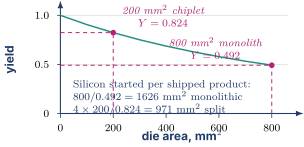
Put a number on it. Take per cm² and a large die of mm², which is 8 cm². Then and
Fewer than half the dies work. Now take a small die of mm², which is 2 cm². Then and . Four out of five work.
Here is the trap, and it is worth walking into deliberately because it is the single most common wrong answer to this question. If you need four of those small dice to build one product, and they are independent, the probability that all four are good is
Exactly the same number as the monolithic die. That is not a coincidence. Under the Poisson model raised to the fourth power is , identically, for any and any . So under the simplest yield model, splitting a die into pieces and requiring all the pieces buys nothing.
If you have ever heard someone say "chiplets improve yield" and stopped there, this is where the argument falls over, and a good interviewer knows it. This is not a straw man, either. The vault's own Trends, Constraints, and Quantitative Principles puts it in exactly that stopped-short form, that splitting a large monolithic die into chiplets "raises overall yield substantially," which is the version most textbook treatments give. So what is the real argument?
1.2 The real argument is silicon consumed per shipped product
The mistake above is the phrase "requiring all the pieces." Nobody fabricates four specific dice and hopes. You fabricate a population of small dice, test them, throw away the bad ones, and assemble products from the good ones. The right metric is therefore not yield, it is how much silicon you had to start in order to end up with one shipped product.
Monolithic. To get one good 800 mm² die you must start of them, consuming
Chiplets. To get one good 200 mm² die you must start of them, consuming mm². You need four, so
Same total function, same total 800 mm² of useful area, and the split consumes 45 percent less silicon. That is the argument, and it survives the Poisson model's multiplicativity because it never required four specific dice to be simultaneously good. Every defect that lands on a monolithic die throws away 800 mm². Every defect that lands on a chiplet throws away 200. The gain is not in the yield number, it is in how much you lose per loss.
Say it in one sentence and it lands: splitting the die does not make defects rarer, it makes each defect cheaper.
1.3 Defects cluster, and the model has to say so
The Poisson model is wrong in a specific and well-documented way. Defects are not sprinkled uniformly. They arrive in clusters: a scratch, a particle shower, an edge effect, a lithography excursion in one region of the wafer. That clustering is modelled by replacing the Poisson distribution with a negative binomial, giving what the literature calls the negative-binomial, Bose-Einstein, or (at a particular parameter value) the Seeds model:
The clustering parameter controls how tightly defects bunch. Small means heavy clustering. As the expression reduces to and you are back to Poisson. Published treatments commonly use somewhere between 2 and 4 for modern processes, with named after Seeds and after Dingwall. The vault's Trends, Constraints, and Quantitative Principles uses and between 0.1 and 0.3 for a mature node, so use here for consistency.
Redo both numbers. Monolithic at cm²:
Chiplet at cm²:
Notice what clustering did. Monolithic yield went up, from 0.449 to 0.492, because a cluster of five defects that would have killed five dice under Poisson now often lands inside one die and kills only that one. A big die is partly protected by clustering, which is genuinely counterintuitive and worth being able to say.
But the silicon-per-product metric still lands on the same side:
A 40 percent reduction rather than 45. The qualitative conclusion is identical under both models, which is exactly the robustness you want before quoting a result.
One honest caveat to volunteer if pushed. Applying the same to a 200 mm² die and an 800 mm² die is an approximation, because is empirically fitted at a particular die size and clustering statistics do not scale perfectly. The direction of the conclusion is not sensitive to that, but the exact percentage is, and saying so is cheap and correct.
1.4 There is a second, quieter gain at the wafer edge
Wafers are round and dice are rectangular, so a ring of partial dice around the circumference is scrapped. The vault gives the standard approximation for gross dice per 300 mm wafer:
where is in mm². The second term is the edge loss, and the thing to watch is the pair of exponents. The interior term falls as while the edge term falls only as , so as the die grows the edge term shrinks more slowly than the quantity it is being subtracted from. Say it in the form that survives a follow-up: a big die loses fewer dice to the edge but a larger fraction of what it could have had.
At : , minus , giving 64.8 gross dice. The edge took 27 percent. At : , minus , giving 306.3 gross dice. The edge took 13 percent.
Four times 64.8 is 259.2, but you actually get 306.3. The split recovers about 18 percent more usable dice from the same wafer purely by fitting the wafer edge better. That is a second-order effect and you should present it as one, but it is real and free.
1.5 The cost equation, and the crossover
Now put money on it. Combine the wafer cost, the dies per wafer, and the yield:
and for the split product, four of those plus a packaging premium that covers the interposer or bridge, the extra assembly steps, and the per-die test that a monolithic part does not need.
Take a wafer cost of $16,000, which sits inside the public range commonly quoted for a leading node, and hold , , and \Delta P = \60$. That packaging premium is an assumption, not a datum. Public estimates for 2.5D assembly vary by more than a factor of three depending on interposer size and volume, so treat it as a dial and watch what it does.
| Monolithic area | Monolithic $ per good die | Four chiplets, silicon only | Plus $60 package | Cheaper |
|---|---|---|---|---|
| 100 mm² | 27.6 | 24.4 | 84.4 | monolithic, by |
| 200 mm² | 63.4 | 51.0 | 111.0 | monolithic |
| 300 mm² | 108.0 | 79.6 | 139.6 | monolithic |
| 425 mm² | 177.7 | 118.3 | 178.3 | dead even |
| 500 mm² | 227.8 | 143.0 | 203.0 | chiplets |
| 800 mm² | 501.7 | 253.6 | 313.6 | chiplets, by 37 percent |
Read the table as a story rather than a lookup. At small die sizes the silicon saving is a few dollars and the packaging premium is sixty, so chiplets are absurd. The silicon saving grows superlinearly with area because yield is convex, and somewhere around 425 mm² it overtakes a fixed sixty-dollar premium. Past that the gap widens fast, and at 800 mm² the split product costs 37 percent less to build.
Now do the sensitivity, because that is what makes the answer credible. Rerun the crossover at other packaging premiums and it moves to roughly 310 mm² at $30 and roughly 590 mm² at $120. So the honest statement is:
With a leading-node wafer, a mature defect density, and a packaging premium somewhere between thirty and a hundred and twenty dollars, the crossover lands between roughly three hundred and six hundred square millimetres. Below that, monolithic. Above it, split.
That is a statement an interviewer can push on and you can defend, because you told them which inputs it depends on before they asked.
Two more things the table quietly teaches. First, the crossover explains an observation you can make from the outside: large server and accelerator parts went chiplet years before phone and laptop parts did, and phone parts largely have not, because a phone SoC is well under the crossover and pays a packaging premium it cannot amortise. Second, the crossover moves down over time, because leading-node wafer cost is rising faster than packaging cost and because packaging volume is driving assembly cost down. Nothing in the argument is a fixed truth about silicon. It is a race between two cost curves.
1.6 The second argument, and it is the stronger one: mixing nodes
Yield is the argument people quote. Node mixing is the argument that actually decides most real partitioning, and it is worth more money.
Here is the physical fact underneath it. Not everything on a die scales at the same rate when you move to a newer process. Logic scales well: smaller transistors, tighter standard cells, real density gain. SRAM has been scaling substantially more slowly than logic for several generations, which is publicly documented and which is why cache area has been growing as a fraction of die area. Analogue and high-speed I/O barely scale at all, because a SerDes needs a certain capacitor to hit a certain noise floor and a certain driver to hit a certain output swing, and physics does not care what node you are on. Electrostatic discharge structures and pads are set by the package, not the transistor.
So a monolithic die on the newest node is paying the newest node's price per square millimetre for a large area that gains nothing from being there.
Work it. Take the same 800 mm² of function, but say 300 mm² of it is logic that genuinely benefits from the leading node and 500 mm² is I/O, SerDes, analogue, and pads that do not. Leading-node wafer $16,000 at . Mature-node wafer, say $5,000 at , both illustrative.
Monolithic, everything on the leading node. From the table, $501.7 per good die, plus a simple package, call it $15. Total $517.
Split by node. Two logic chiplets of 150 mm² on the leading node: DPW, and , so 360.0 good per wafer at $44.4 each, $88.9 for two. Two I/O dice of 250 mm² on the mature node: DPW, and , so 212.8 good per wafer at $23.5 each, $47.0 for two. Silicon total $135.9, plus the $60 advanced package. Total $196.
A 62 percent reduction, and notice what did not happen: nothing got smaller, nothing got faster, no transistor was saved. The same silicon was simply bought where it was cheapest. That is why this argument beats the yield argument in practice, and why the first partitioning question on a real product is almost never "where does the yield curve say to cut" but "what on this die does not want to be on the expensive node."
The corollary is a design rule you can state in one line and that a lot of candidates cannot: an I/O die is the single most obvious chiplet in any system, because I/O is the largest block whose cost per square millimetre is highest and whose benefit from the new node is lowest.
1.7 The third argument, reuse across a product family
The third argument is amortisation of non-recurring engineering, and it is the one that a company's finance organisation cares about most.
A tapeout at a leading node costs a mask set plus a design and verification programme. Public estimates for leading-node mask sets run to tens of millions of dollars and for total design cost of a large SoC into the hundreds of millions. The numbers are contested and vary enormously with design size, so do not quote a specific one in an interview. What matters is the structure, and the structure is clean enough to state without any dollar figure at all.
Suppose you want four products: a one-socket part, a two-socket part, a four-socket part, and an eight-socket part, differing in compute capacity and sharing everything else. Monolithically that is four separate die designs, four tapeouts, four verification programmes, four sets of masks, four physical-design closures. With chiplets it is two die designs: one compute chiplet and one I/O chiplet. The four products are then assembly-level configurations that differ in how many compute chiplets go on the substrate.
If a die design costs units of engineering, you moved from to and you covered the same four SKUs. And you did something the cost model does not capture. You decoupled the schedules. The compute chiplet can respin on a new node without touching the I/O chiplet, which means the expensive, risky, schedule-driving piece is smaller and the boring piece is reused.
The cost of this is a real constraint most people miss. Reuse only works if the interface is frozen, and freezing an interface early is precisely what an architecture team hates doing. A die-to-die interface that changes between the compute chiplet and the I/O chiplet destroys the entire reuse argument, which is a large part of why a standard interface with a compliance programme is worth so much, and it is the natural bridge into Part 5.
1.8 What the three arguments do not say
Keep the negative space clear, because it is where the follow-up lives.
Chiplets do not make a chip faster. A monolithic die of the same function is faster, lower power, and lower latency than the same function split across a package, always, with no exceptions. The split is a cost decision that you then pay for in performance, and the whole engineering discipline of Parts 2 through 8 is about paying as little as possible.
Chiplets do not reduce total silicon area. They increase it, because each die now needs its own die-to-die PHYs, its own power delivery, its own seal ring and scribe-line allowance, and its own test structures. Part 2.5 puts a number on that.
And chiplets do not make a design simpler. They convert an on-die wire into a protocol, and protocols have training, retry, flow control, error handling, and version negotiation. That is the trade, and being able to state it in that shape is the difference between a candidate who has read a press release and one who has thought about it.
02.Part 2, the costs, stated honestly
Every one of these is a question an interviewer will reach for after you deliver Part 1, because Part 1 is the sales pitch and they want to know whether you have heard the objections.
2.1 The link burns energy that a wire did not
An on-die wire between two blocks costs whatever its capacitance costs and nothing else. There is no protocol, no serialiser, no clock recovery, no cyclic redundancy check. The moment those blocks are on different dice, every bit that crosses pays for a transmitter, a receiver, a sampling clock, and a share of the digital logic that keeps the link alive.
Part 4 works the arithmetic. The short version is that a good die-to-die link costs somewhere between about a quarter and one picojoule per bit depending on reach and packaging, which is roughly an order of magnitude better than a long-reach serialiser-deserialiser, and rather more than that at the advanced-package end, but is still not free the way an on-die wire is.
Turn that into a system number, because that is what makes it real. Suppose two dice exchange 1 terabyte per second, which is bits per second, at 0.5 pJ per bit:
Four watts of pure interconnect, doing no computation, that a monolithic design would not have spent. On a 300 W part that is one and a third percent and nobody notices. On a 15 W mobile part it is 27 percent and it kills the product. That single calculation is most of the reason phone-class parts have largely stayed monolithic, and it connects the packaging decision to the power budget in exactly the way Power Fundamentals and Clock Gating connects everything else.
2.2 Latency across a boundary is real and it is not the flight time
The instinctive worry is the speed of light, and the instinctive worry is wrong. Compute it and dismiss it.
A signal on an organic package substrate propagates at roughly with a relative permittivity near 3.5 to 4, giving something in the region of 6 to 7 picoseconds per millimetre. Twenty-five millimetres, which is about as far as a standard-package die-to-die link is specified to reach, is therefore about 160 picoseconds. On a silicon interposer at 2 mm it is about 13 picoseconds. Both are trivial next to a 3 GHz clock period of 333 ps.
So where does the latency come from? From the protocol, and it stacks up like this:
Serialisation. Data must be gathered into whatever unit the link moves. If the link carries a 256-byte flit and runs at 256 GB/s, gathering one flit takes exactly 1 ns before anything is transmitted.
Transmit path. The physical layer must retime the data into the transmit clock domain, drive it, and forward a clock alongside it.
Receive path. Sample, deskew per lane, deserialise, and realign into a flit.
Error checking. The cyclic redundancy check covers a whole flit, so it cannot be evaluated until the last byte of that flit has arrived. If the receiver refuses to forward a flit before the check passes, that is a store-and-forward delay of one full flit time, another 1 ns in the example above. If it forwards optimistically and cancels on failure, it has pushed the problem into the consumer, which is a design choice with its own consequences.
Clock domain crossing. The receiving die's core logic runs on its own clock, unrelated to the forwarded clock. Two flops of synchroniser at 2 GHz is 1 ns of pure latency, on top of the asynchronous FIFO's own occupancy.
Add them and a one-way crossing lands in the low single-digit nanoseconds, with published vendor claims varying and with the total depending strongly on flit size, frequency ratio, and whether the design chose store-and-forward or cut-through. Do not quote a specific number as though it were a specification. Do say that the flight time is negligible and the protocol pipeline is everything, because that is the insight and it is stable.
Then translate it. A round trip is two crossings, so call it under ten nanoseconds if the link is good. At 3 GHz that is roughly thirty core cycles added to anything that has to go across and come back. For a bulk data transfer, invisible. For a coherent request that must reach a directory on another die and return, it is the difference between a 25 ns and a 45 ns hit, and Part 7 is about what that does.
2.3 Testing gets much harder, and "known good die" is the whole problem
This is the cost that surprises people, and it is where your DFT background becomes an asset rather than a liability.
In a monolithic flow you test the wafer, you package the good dice, you test the packaged part, and a part that fails final test costs you one package. In a chiplet flow you assemble several dice into one package, and if any one of them is bad you have thrown away all the others plus the interposer plus the assembly. The economics of Part 1 assumed you only assemble good dice. That assumption has a name, known good die, and delivering it is a research-grade problem.
Why is it hard? Because wafer-level probe test is genuinely weaker than packaged test, for reasons that are physical rather than procedural.
Probe cards contact pads mechanically, and at the bump pitches of Part 3 a probe needle is comparable in size to the bump. Fine-pitch probing is possible but it is slow, it damages bumps, and it limits how many pads you can contact at once, which limits parallel test and therefore test time and therefore cost. Probe contact resistance is worse than a soldered joint, so at-speed I/O test through a probe card is limited. Wafer-level thermal control is poorer than package-level, so you cannot easily test at the temperature corners where marginal parts fail. And a die at wafer sort has not yet experienced the mechanical and thermal stress of assembly, which is exactly the stress that turns a marginal defect into a failure.
The consequence is that the yield you can demonstrate at wafer level is lower than the yield the die actually has, and the gap is what you pay for. That gap is why per-die test cost belongs in in Part 1.5, and why the crossover moves when your test capability changes.
There is a second-order effect worth naming because it shows systems thinking. If each die's known-good probability is and you assemble of them, the probability that the assembly is built entirely from good dice is , and the assembly yield multiplies on top of that. At and you are already down to before assembly defects. So the escape rate at die test enters the product cost raised to the power of the chiplet count, which is a strong argument for spending on test and a strong argument against very high chiplet counts.
Part 8.6 covers what you build into the RTL to make this tractable.
2.4 Thermal and mechanical problems multiply
Two dice side by side on a substrate share a heat spreader and a power delivery network, and they interact. Two dice stacked interact much more.
The stacking problem is a thermal series resistance problem. Heat leaves a die through its back side into a thermal interface material and then into a lid or heat sink. Put a second die on top of the first and the lower die's heat must now travel through the upper die, through the bond interface, and through everything above, before it reaches the sink. The literature on 3D thermal management is consistent that upper dice see higher thermal resistance to the sink, and that in logic-on-logic stacks the die in the middle can end up hottest of all, because it is heated from below and insulated from above.
That has a direct architectural consequence: you cannot stack two high-power dice. What you can stack is a high-power die on a low-power one, which is why the publicly described 3D logic products put compute on top of a base die holding cache, I/O, and power delivery, rather than compute on compute. If an interviewer asks how you would partition for a 3D stack, "put the power density where it can get out" is the first-order answer.
Then the mechanical half, which is genuinely a different failure mode. Silicon has a coefficient of thermal expansion around 2.6 parts per million per kelvin. Copper is around 17. An organic build-up substrate sits in the same region as copper in the plane of the package, roughly 15 to 20, and is far higher than that through its thickness. The mismatch that matters is not copper against substrate, it is everything against silicon, and that is a factor of six or more at every interface. Heat the assembly and the layers want to grow by different amounts, and the mismatch shows up as stress concentrated at exactly the small features you care about: microbump joints, through-silicon via sidewalls, hybrid-bond interfaces, and underfill. Repeated thermal cycling drives warpage, void formation in vias, delamination, and cracking. This is why chiplet products carry reliability qualification requirements that a monolithic part does not, and it is why the automotive-oriented additions to the die-to-die standards, which include health monitoring and predictive failure analysis, exist at all.
There is a subtler stress effect that connects to your doctoral work. Local mechanical stress changes carrier mobility, which changes transistor drive strength, which changes timing. Stress near a through-silicon via is a documented enough phenomenon that physical design tools enforce a keep-out zone around each via, in which standard cells may not be placed. That is area you lose that has nothing to do with the via's own footprint, and mentioning it is a strong signal that you have thought past the block diagram.
2.5 And it costs area, which nobody puts in the slide
Split one die into four and you have added, per die: a seal ring and scribe-line allowance, its own power delivery entry points and decoupling, its own clock generation or clock distribution entry, its own reset and test infrastructure, and one or more die-to-die PHYs with their bump fields.
The PHY bump field is the interesting one because it is not a soft cost. A die-to-die interface is laid out along the die edge, because that is where the neighbouring die is, and the number of lanes you can bring out is set by how many bumps fit along that edge. The industry word for die edge available to an interface is shoreline or beachfront, and it is a genuinely scarce resource: a die has only four edges and every interface wants one.
So a chiplet design has a constraint monolithic designs do not: the floorplan is partly dictated by which blocks need to talk across the boundary, because the ones that do must sit near an edge. That constraint is real, it is unfamiliar, and it is the kind of thing a physical-design-aware interviewer will probe.
03.Part 3, packaging from first principles
Everything above assumed a package exists and costs money. Now build it up from nothing, because the packaging choice determines the bump pitch, the bump pitch determines the interconnect density, and the interconnect density determines what kind of link you can build at all.
3.1 What a package is actually for
Strip it to function. A bare die is a fragile piece of silicon about three quarters of a millimetre thick, with connection pads whose spacing is measured in tens of microns. A circuit board has features measured in tens of thousandths of an inch, which is to say hundreds of microns, because that is what a board can be etched and assembled at economically.
So a package does exactly one essential thing. It is a fan-out, a mechanical and electrical translator from the die's fine pitch to the board's coarse pitch. Everything else it does follows from having to exist for that reason, whether that is protecting the die, spreading heat, or providing a place to put decoupling capacitors.
Older packages did the fan-out with wire bonds, thin gold or copper wires from pads around the die's perimeter up to the package. Wire bonds are cheap and they are still everywhere in low-cost parts, but they are perimeter-only, so pad count scales with die perimeter rather than die area, and each wire is a millimetre or more of inductive loop, which is fatal for both signal integrity and power delivery at any speed.
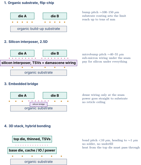
Flip-chip replaced them for anything high performance. Instead of pads around the edge, the die grows an array of solder bumps across its whole face, and it is flipped over and soldered directly onto the package substrate. Now pad count scales with die area, the connection is a short vertical bump rather than a long wire, and the power delivery network can inject current in the middle of the die rather than only around the edge. Flip-chip bump pitch on an organic substrate is typically in the region of 100 to 150 microns, set by what the substrate underneath can route.
Hold that number, because everything in this part is a fight to make it smaller.
3.2 The organic substrate, and what its routing rules buy
The standard package substrate is a laminate: layers of organic resin with copper wiring, built up much like a fine printed circuit board. Its wiring capability is described by line and space, the width of a copper trace and the gap to the next one. High-end build-up substrates are publicly described in the range of a few microns of line and space at the aggressive end, with more typical production values coarser than that.
Now do the arithmetic that makes the packaging ladder make sense. Suppose you must route escape wiring out from under a bump field at 110 µm pitch. Between two adjacent bumps you have 110 µm of width minus the bump's own pad. Call the pad 45 µm and about 65 µm of clear channel is left. At 8 µm line and 8 µm space each trace consumes 16 µm of that channel, so traces fit through the gap per layer. Multiply by the number of routing layers and that sets how many signals can escape per millimetre of die edge.
That is why the standard-package die-to-die interface exists as a distinct, coarser mode: the constraint is not the die, it is what the substrate can route out from under the die. A finer bump pitch is useless if nothing can be wired to it.
What the organic substrate buys you in return is everything the others do not: it is cheap, it is mature, it is mechanically compliant, it can be large, and it can carry a signal 25 mm or more. What it costs you is density.
3.3 The silicon interposer, which is 2.5D
If the substrate's wiring is the limit, put something with better wiring underneath the dice. A silicon interposer is a large, deliberately simple silicon die, with no transistors or very few, that carries several layers of damascene copper wiring at on-chip dimensions, meaning line and space measured in fractions of a micron rather than microns. The compute dice are mounted face-down on the interposer with fine microbumps. The interposer is mounted on the ordinary organic substrate with ordinary flip-chip bumps. Vertical through-silicon vias carry power and low-density signals from the substrate up through the interposer to the dice.
The name 2.5D is a deliberate joke that is also an accurate description. It is not 3D because no active die sits on top of another active die. Every die is face-down in the same plane. But it is not 2D either, because there is a silicon layer beneath doing routing that a substrate could never do. TSMC's CoWoS, meaning chip-on-wafer-on-substrate, is the best-known public example of this construction.
What it buys is enormous. Microbump pitch drops to roughly 40 to 55 microns, and the wiring underneath is on-die-quality, so you can bring out an order of magnitude more signals per millimetre of shoreline and each of them sees a short, well-controlled, low-capacitance wire. That is exactly the regime that makes the advanced-package die-to-die mode of Part 5 possible.
What it costs is an extra large silicon die, fabricated and thinned and through-via'd. It costs an extra assembly step with its own yield. It costs a hard limit on how big the interposer can be, since it is patterned by the same steppers as any other die and therefore cannot exceed a reticle field without stitching. And it costs warpage risk from putting a large thin sheet of silicon between two things with different expansion coefficients.
The economic complaint about an interposer is easy to state: you are paying for silicon area under the whole assembly, including the large regions where you only needed power delivery. That complaint is the entire motivation for the next option.
3.4 Embedded bridges, which buy the density only where it is needed
Notice that the high-density wiring is only needed between the dice, in a strip near the shared edge. Everywhere else, ordinary substrate routing is fine. So instead of a full interposer, embed a small piece of silicon inside the organic substrate, positioned exactly under the seam between two dice, and let it carry the dense wiring locally while the rest of the connections go straight into the substrate as usual. Intel's publicly described EMIB, the embedded multi-die interconnect bridge, is the best-known implementation of this idea.
What it buys is the interposer's local wiring density at a fraction of the silicon area, no through-silicon vias in the main current path for power (power goes straight from substrate to die, not up through an interposer), and no reticle-size ceiling on the overall package.
What it costs is a substrate process that can embed and align a silicon die inside a laminate to micron accuracy, which is a genuinely difficult manufacturing capability, plus a floorplanning constraint: the high-density connections must be located over the bridge, which is a narrow region, so a designer no longer has freedom about where the die-to-die interface sits.
The comparison to state in an interview is one sentence: an interposer gives you dense wiring everywhere and charges you for silicon everywhere, and a bridge gives you dense wiring where the seam is and charges you only there. Which is better depends on how much of the assembly's total wiring is die-to-die versus die-to-board, and that is a property of the product.
3.5 True 3D, through-silicon vias, and hybrid bonding
Everything so far kept every die in one plane. 3D means stacking active dice on top of each other, and it changes the interconnect from a horizontal wire to a vertical connection a few tens of microns long.
Two mechanisms. The older one keeps solder in the picture: thin the upper die, punch through-silicon vias through it, and connect the stack with microbumps. Public figures put through-silicon vias at around 5 µm diameter through a die thinned to around 50 µm, and microbump pitches for stacking in the region of 25 to 40 µm, with the literature noting that solder microbump pitch is hard to scale much below the tens of microns because solder volume, bridging, and joint reliability all get worse as the joint shrinks.
The newer one removes solder entirely. Hybrid bonding polishes two wafer or die surfaces to atomic flatness, each with an oxide field and recessed copper pads, and bonds them directly: oxide to oxide by dielectric bonding, then a thermal anneal that expands the copper into contact so copper meets copper. There is no solder, no underfill, and no bump. Public descriptions place hybrid-bond pitch below 10 µm today and heading toward the low single digits and eventually the region of 1 µm, and TSMC's SoIC and Intel's Foveros Direct are the publicly named implementations.
Do the density arithmetic once and the significance is obvious. Connection density goes as the inverse square of pitch, so moving from a 40 µm microbump to a 4 µm hybrid bond is a factor of
a hundred times more connections per square millimetre. And the connection itself is a micron-scale copper stub with a capacitance in the region of a femtofarad rather than a bump with tens of femtofarads. That is the regime where the die-to-die link stops looking like a link and starts looking like a wire, which is what makes the 3D die-to-die mode in Part 5.6 a genuinely different animal with a much lower energy per bit.
What it costs is everything. Wafer-level flatness and cleanliness requirements that are extreme even by semiconductor standards, because a single particle ruins a bond over a large area. Copper grain structure control, because the anneal-driven expansion has to be uniform. And, most importantly for the economics of Part 2.3, hybrid bonding is hostile to known-good-die. If the process is wafer-to-wafer, you are bonding whole wafers including the bad dice, and the composite yield is the product of the two wafers' yields die by die. Die-to-wafer bonding recovers the ability to place only known-good dice, at the cost of throughput.
3.6 The ladder, summarised
| Construction | Typical connection pitch | Wiring available between dice | Practical reach | Relative cost |
|---|---|---|---|---|
| Organic substrate, flip-chip | ~100 to 150 µm | substrate build-up layers, microns of line and space | tens of mm | baseline |
| Silicon interposer, 2.5D | ~40 to 55 µm microbump | on-die damascene, sub-micron | a few mm | high, silicon under everything |
| Embedded bridge | ~40 to 55 µm microbump | on-die damascene, locally | bridge length | between the two |
| 3D microbump stack | ~25 to 40 µm | vertical, through-silicon vias | tens of µm | high |
| 3D hybrid bond | below 10 µm, trending toward ~1 µm | vertical, copper to copper | a few µm | highest |
Every pitch figure here is a public order-of-magnitude range and every one of them moves year to year. What does not move is the ordering and the reason for it, and that is what to carry into an interview.
04.Part 4, the physical link, and picojoules per bit
Now connect the packaging to the electrical design, because the entire reason to care about bump pitch is that it changes what kind of transmitter you are allowed to build.
4.1 A die-to-die link is not a SerDes, and the reason is reach
Start with the thing it is not. A long-reach serialiser-deserialiser, the kind that carries PCIe or Ethernet across a board and through connectors, faces a channel with tens of decibels of loss at the Nyquist frequency. To get a signal through that channel it needs: a large output driver, transmit equalisation to pre-distort the signal, receive equalisation with a continuous-time linear equaliser and usually a decision-feedback equaliser, and a clock and data recovery loop, because after that much channel there is no usable forwarded clock. All of that is analogue circuitry that runs continuously, and it is why long-reach SerDes energy sits in the single-digit picojoules per bit, with published figures for the fastest generations in the range of several picojoules per bit.
Now change one thing. Make the channel 2 mm of clean silicon interposer wiring instead of 30 cm of lossy board. The channel loss essentially disappears. And once the loss disappears, so does the justification for every circuit above.
Do the flight-time arithmetic to see why this is a hard boundary rather than a matter of degree. At roughly 6.5 ps per millimetre:
- 2 mm of interposer is about 13 ps of flight. At 32 GT/s the bit period is ps. Flight time is under half a bit period, so at any instant there is less than one bit in flight on the wire. The wire behaves as a lumped capacitor. You can drive it with a plain inverter, unterminated, and pay .
- 25 mm of substrate is about 160 ps, which is five bit periods. Five bits are on the wire simultaneously. The wire is now a transmission line, reflections from an unterminated far end will arrive back in the middle of subsequent bits, and you must terminate it. A terminated line burns static current whenever it is driven, whether or not anything is switching.
That is the whole story of why reach dominates energy, and it is a much better answer than "shorter wires have less capacitance." Shorter reach lets you delete the termination, the equaliser, and the clock recovery, and those are where the energy was.
Two more consequences follow from the same fact and both are worth naming. First, because the channel is clean and short, a die-to-die link can forward its clock alongside the data rather than recovering it, which removes the phase-locked loop and clock-data-recovery loop from the receive path and removes their latency too. Second, because it does not need a fast serialiser to overcome pin scarcity, it can be wide and slow rather than narrow and fast: many parallel lanes at a modest rate instead of a few lanes at an extreme one. Wide and slow is much more energy-efficient per bit, and it is only affordable because the packaging gave you the bumps.
4.2 Bump pitch to bandwidth density, worked
The figure of merit for how much a link buys you per unit of die edge is shoreline bandwidth density, in gigabytes per second per millimetre of die edge. Build it from the pitch.
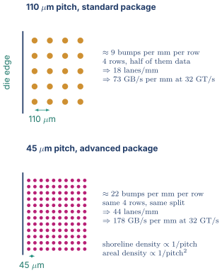
Take a standard-package pitch of 110 µm. Along one millimetre of die edge you fit
The PHY's bump field is several rows deep. Take four rows, so 36.4 bumps per millimetre of shoreline. Not all of them carry data: you need power, ground, the forwarded clock, a valid signal, the sideband, and any spares. Assume half are data lanes, so 18.2 lanes per millimetre. At 32 GT/s per lane:
Now the advanced-package pitch of 45 µm. Along one millimetre you fit bumps per row, four rows gives 88.9, half are data gives 44.4 lanes per millimetre, and
Public UCIe material quotes shoreline density in the region of 28 to 224 GB/s per mm for the standard package and 165 to 1317 GB/s per mm for the advanced package, the wide ranges reflecting different data rates and bump-field depths. Both of the numbers above land inside their respective published ranges, which is the check you want on a hand calculation.
One scaling relationship is worth getting exactly right because it is a favourite follow-up. Shoreline density scales as . Areal density scales as . You can verify which one a published figure means. The UCIe material states that moving from a 45 µm bump pitch to 25 µm gives higher density, and
exactly, so that particular claim is areal. Being able to do that check out loud, in a sentence, is a small thing that signals you read specifications rather than summaries of them.
4.3 Picojoules per bit, derived rather than quoted
The standard figure of merit for a link's efficiency is energy per bit, measured in picojoules. Define it precisely first, because a sloppy definition is where the follow-up lands. It is the total energy the link consumes divided by the number of payload bits it delivered, and "total" should include the transmitter, the receiver, the clocking, and the digital logic of the link layer. A number that counts only the output driver is not comparable to anything.
Now derive a floor for the advanced-package case using nothing but Power Fundamentals and Clock Gating Part 1.1. Charging a capacitance from 0 to takes from the supply. For random data, a given lane makes a transition on average once every four bits, so
Estimate . Two millimetres of interposer wiring at roughly 0.2 pF per mm is 0.4 pF, plus a microbump, a pad, and the receiver input, call it 0.1 pF. So pF. At a swing of V,
Public UCIe material gives an advanced-package efficiency target in the region of 0.25 pJ per bit. So the wire itself is about a quarter of the budget and the remaining three quarters is transmitter and receiver circuitry, the sampling clock, the deserialiser, and the digital link logic. That ratio is the whole design insight for this regime. At short reach, shrinking the wire further buys you almost nothing unless you shrink the PHY with it.
Now the standard-package case, where the transmission-line analysis of 4.1 applies. A terminated line of characteristic impedance driven with a swing burns roughly while it is being driven, and with random data it is driven about half the time:
At 32 Gb/s that is pJ per bit for the termination alone, before driver inefficiency, equalisation, or any of the receive path. Public UCIe material gives a standard-package target in the region of 0.5 pJ per bit, so again the wire is a modest fraction and the circuitry is most of it.
The comparison table that follows is the one worth memorising, and every entry in it is a public order-of-magnitude range rather than a specification:
| Link | Reach | Approximate energy per bit |
|---|---|---|
| On-die global wire | mm | well under 0.1 pJ, and no protocol at all |
| Die-to-die, hybrid-bonded 3D | µm | publicly described as far below the 2D figures, so treat it as a small fraction of 0.1 pJ and hedge |
| Die-to-die, advanced package | ~2 mm | ~0.25 pJ, which is the published UCIe target rather than a measured range |
| Die-to-die, standard package | up to ~25 mm | ~0.5 pJ published target, and real parts land between that and roughly 1 pJ |
| Long-reach SerDes, board and connector | cm to tens of cm | single-digit pJ |
Every number in that column moves with process, voltage, and data rate. What does not move is the ordering and the ratios, and the sentence that explains them: energy per bit is set by reach, because reach decides how much analogue machinery the channel forces you to build.
05.Part 5, UCIe as a public standard
Now the specific thing an interviewer will name. Describe it from the published specification material only, and hedge version-specific details, because the specification has revised several times and the person across the table is probably working against one particular revision.
5.1 What the standard is, and what it is not
UCIe, Universal Chiplet Interconnect Express, is an open industry standard for connecting dice inside a single package. It was introduced in 2022 by a consortium whose founding members include most of the large processor, foundry, and packaging companies, and it has revised several times since. The publicly documented sequence is 1.0, then 1.1, then 2.0 which added a manageability and debug architecture and support for 3D packaging, then 3.0 which was announced in August 2025 and adds 48 and 64 GT/s data rates along with manageability and sideband-reach extensions. Each revision is described as backward compatible with the previous ones. Do not assert a feature's revision number unless you are certain. Say "recent revisions added" and let the interviewer supply the number.
Three things it is not, and getting these right prevents the most common category error.
It is not a memory protocol and not a board-level protocol. Nothing about UCIe appears on any pin that leaves the package. It is an internal chip-to-chip boundary in exactly the way DFI is an internal controller-to-PHY boundary in DRAM Controllers JEDEC and DFI.
It is not a coherence protocol. It carries one. It does not define one. Part 7 is about what that distinction costs.
It is not a packaging technology. It is defined over packaging technologies that already exist, and the specification's job is to define what a compliant transmitter and receiver look like at a given bump pitch so that two dice from two companies interoperate.
That last point is the actual product being sold. The technical content is not radical. Parallel clock-forwarded die-to-die links existed before it. What did not exist was an interoperability contract with a compliance programme, and without one the reuse argument of Part 1.7 cannot be realised across company boundaries. State that and you have answered "why does this standard matter" better than a feature list would.
5.2 The three layers, and why the split is where it is
UCIe is defined as three stacked layers, and the interesting question is not what they are called but why the boundaries fall where they do.
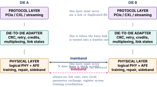
The physical layer is the electrical interface to the package plus the digital logic that owns it. There are three publicly described components. First, the analogue front end, meaning the transmitters and receivers. Second, a logical PHY that runs link initialisation, training, and calibration and implements test and repair. Third, a sideband channel used for parameter exchange and negotiation between the two dice. The design principle is that this layer is protocol-agnostic. It moves bits and knows nothing about what they mean.
The die-to-die adapter is the intermediate layer, and it is the interesting one. Public descriptions of its responsibilities are consistent: flit framing and mapping, CRC generation and checking, link-level retry for reliable delivery, credit-based flow control, protocol multiplexing so that more than one protocol can share a link, and link power-state management.
Read that list again and notice what it is. It is precisely the set of jobs required to turn a channel that can drop a bit into a channel that cannot. That is why the boundary is where it is. The protocol layer above is a coherence or transaction protocol that was designed for an on-die fabric where wires do not corrupt data, and it would be a disaster to teach it about bit errors. So the adapter absorbs the entire problem and presents an interface with the same guarantees an on-die fabric has: no loss, no duplication, and order preserved.
The protocol layer hosts whatever is actually being carried. Publicly named options are PCIe, CXL, and a raw streaming mode that carries anything else. Streaming is the important one for a chiplet designer, because it is the escape hatch. If what you want to move across the package is your own fabric protocol or a standardised coherence protocol like Arm's CHI Chip-to-Chip, streaming is the mode that carries it.
5.3 Inside the physical layer: modules, lanes, clock, and sideband
The physical layer is organised into modules, a module being the unit of link that trains and operates together. Public descriptions give the standard-package module as 16 lanes and the advanced-package module as 64 lanes, with multiple modules aggregated to reach the bandwidth a product wants.
Alongside the data lanes each module carries a forwarded clock, a valid signal marking when data on the lanes is meaningful, and a track signal used for per-lane drift correction at higher rates. The forwarded clock is the point of 4.1. Because the channel is clean and short, the transmitter can simply send its clock alongside the data and the receiver does not need to recover it.
The sideband is separate and is worth understanding properly because it answers several interview follow-ups at once. It is described as a forwarded clock pin and a data pin in each direction, running at a low fixed rate, and it is used for parameter exchange, register access for debug and compliance, and coordination of link training and management with the partner die.
Why does a separate low-speed channel exist at all when there is a perfectly good high-speed one right next to it? Because of a bootstrap problem. The mainband is not usable until it has been trained, and training requires the two dice to agree on data rate, lane mapping, and repair configuration. That negotiation has to happen over something, and it has to be something that works before anything has been configured. So the sideband runs at a rate slow enough to work with no training at all, and it is the channel of last resort for debug when the mainband is broken. If you ever have to bring up a die-to-die link in a lab, the sideband is the only thing you have.
5.4 Inside the adapter: CRC, retry, credits, multiplexing
This is the layer an RTL designer would most likely be asked to build, so it is worth being concrete.
Flits. Data crosses the link in fixed-size units. Public descriptions of the UCIe flit formats include a raw 64-byte format with no CRC or retry bytes, a 68-byte format consisting of 64 bytes of payload with a 2-byte header and a 2-byte CRC added by the adapter, and several 256-byte formats including latency-optimised variants that trade payload bytes against CRC and header overhead. Treat the exact byte splits as version-dependent and do not recite them. What you should be able to explain is why a family of formats exists rather than one. A small flit has lower store-and-forward latency and higher header overhead, a large flit is the reverse, and different protocols and products sit at different points on that trade.
CRC and retry. The adapter computes a cyclic redundancy check across each flit on transmit and verifies it on receive. On a mismatch it requests replay, and the transmitter resends from its replay buffer. Public material describes a detection guarantee expressed in terms of the number of random bit errors detected. Do not quote a specific polynomial or guarantee unless you have the specification open.
Two design consequences you should be able to derive on the spot. First, the replay buffer must hold every flit that has been transmitted but not yet acknowledged, so its size is the bandwidth-delay product of the acknowledgement loop. At 256 GB/s and a 20 ns round trip that is bytes, so roughly 5 kB of buffer per direction, and it grows linearly with both rate and latency. Second, the sequence-number space must exceed the maximum number of unacknowledged flits by a comfortable margin, or a wrapped sequence number can be mistaken for a fresh one.
Credit-based flow control. The receiver advertises buffer credits. The transmitter may only send when it holds a credit. The receiver returns credits as it drains. This is exactly the mechanism from Interconnect and AMBA Part 7, moved across a package. The reason it must be credits rather than a backpressure signal is latency. A stop signal takes a full round trip to take effect, so by the time it arrives the transmitter has already sent a round trip's worth of data, and the receiver would need that much buffering anyway. Credits make the buffering explicit and let you size it.
Multiplexing. More than one protocol can share a link, which means the adapter is also an arbiter, and everything from Arbiters FIFOs and CAMs about fairness and starvation applies.
Link power states. The adapter manages low-power states, publicly named L1 and L2, and it must sequence entry and exit with the partner die. This is a distributed power-sequencing problem, which is the Power Fundamentals and Clock Gating Part 7.4 discipline applied across a package boundary where the two halves cannot see each other's rails.
5.5 The protocol layer, and why streaming matters most
Public material names PCIe and CXL as directly supported protocols, plus a raw streaming mode. CXL itself is CXL and Coherent Memory Expansion's subject and is worth reading alongside this section, because the coherent-attach semantics it defines are exactly what the streaming discussion below is an alternative to. The value of native PCIe and CXL support is that an enormous amount of existing IP and software already speaks them, so a chiplet exposing a PCIe interface across the package is immediately usable.
For a chiplet-based CPU or accelerator, though, streaming is the mode that matters, because what you want to send is your own fabric's traffic. The publicly described example worth knowing is Arm's AMBA CHI Chip-to-Chip, announced in 2024, which extends the on-chip CHI coherence protocol across a package and is explicitly described as being transported over UCIe's streaming interface. That is the architecture to have in your head for a coherent multi-chiplet CPU: the coherence protocol is CHI or something like it, the transport is UCIe streaming, and the adapter in between is what makes the transport look lossless enough for a coherence protocol to survive on it.
5.6 Standard, advanced, and 3D modes
The specification defines the same architecture and the same protocols across several packaging regimes, differing in the bump map and the PHY organisation. Public descriptions give:
| Mode | Bump pitch | Reach | Module width | Energy target | Repair strategy |
|---|---|---|---|---|---|
| Standard package | ~100 to 130 µm | up to ~25 mm | 16 lanes | 0.5 pJ/bit target | no spare lanes, degrade width |
| Advanced package | ~25 to 55 µm | up to ~2 mm | 64 lanes | 0.25 pJ/bit target | spare lanes for repair |
| 3D | ~10 to 25 µm down to ~1 µm | vertical, µm | optimised for hybrid bonding | described as substantially better | see specification |
Two details in that table are worth pulling out because they are exactly the kind of thing that separates candidates.
First, the repair strategies genuinely differ, and the reason is bump budget. Public descriptions state that an advanced-package x64 module is organised as two groups of 32 data lanes, each group with two spare lanes, so up to two failed lanes per group can be repaired independently. The standard-package x16 module has no spare lanes at all. Instead, a failure causes the link to degrade in width, from x16 to x8 to x4. The reason is that at 110 µm pitch every extra bump is expensive shoreline, and adding spares costs more than the repair is worth, whereas at 45 µm a spare bump is cheap. That is a clean example of a packaging parameter propagating all the way into a protocol feature.
Second, some signals have no repair and no degradation path. Public descriptions note that a failure of the forwarded clock, the valid signal, the track signal, or the sideband is fatal for that module, and the response is to route traffic through other modules. That tells you something structural about how to build a product: module count is your redundancy granularity, and a design with one module has no graceful degradation at all.
5.7 What to hedge, and how to hedge it
The specification has revised repeatedly and the details that move are exactly the ones that sound impressive: data rates, flit format byte counts, feature-to-revision mapping, and compliance requirements. The professional posture is to be fluent about structure and explicitly approximate about constants.
A sentence that works: "As of the revisions I have read, the advanced package targets something in the region of a quarter of a picojoule per bit at bump pitches in the forties of microns, and the data rate ceiling has moved up at least twice since 1.0. If we are designing against a specific revision I would want the document open, because those numbers have all moved."
That sentence costs nothing, and it is much better than a confident wrong figure. An interviewer who works on this every day will know instantly which of the two you are.
06.Part 6, the other public approaches, and what each solves
UCIe is not the only die-to-die interface and an interviewer may test whether you know that. The right level of knowledge here is what problem each one was built to solve, not the pinout.
Bunch of Wires, developed in the Open Compute Project's Open Domain-Specific Architecture group, is an open parallel die-to-die PHY specification. Its distinguishing choice is that it was explicitly designed to work well on ordinary organic substrates rather than requiring silicon interposers, which is a deliberate cost position. It is defined as a set of unidirectional slices carrying 16 bits each, aggregated to reach the throughput you need, source-synchronous with a forwarded differential clock, in a family of modes from BoW-32 up to BoW-512 whose per-slice rates span an order of magnitude. Its published energy targets sit in the region of under 0.5 to 1 pJ/bit for doubly terminated modes and under 0.25 to 0.5 pJ/bit for unterminated ones, which is the same physics as Part 4.1 and lands in the same place. The problem it solves: give the ecosystem a low-cost open PHY that does not force anyone to buy an interposer.
Advanced Interface Bus, originally developed at Intel and contributed publicly with its 2.0 specification placed in the CHIPS Alliance repository, is a parallel clock-forwarded die-to-die interface that predates UCIe and was used in publicly described multi-die FPGA products. The problem it solves: it was an early existence proof that a wide, slow, unterminated parallel link across a package was a better answer than a SerDes, and it fed the thinking that produced the later standards.
High Bandwidth Memory is not usually described as a die-to-die interface but it is the field's most important existence proof and it is worth citing. HBM connects a stack of DRAM dice to a processor across a silicon interposer using a 1024-bit-wide interface at a comparatively modest per-pin rate. That is exactly the wide-and-slow trade of Part 4.1, arrived at independently and shipped in volume for years before chiplet standards existed. If an interviewer asks whether wide parallel die-to-die links are practical, HBM is the answer. They have been shipping in enormous volume for a decade.
Proprietary links. Several vendors have publicly described their own die-to-die interconnects for their own products, and public product disclosures and keynote material are fair to discuss. Two rules for an interview. First, discuss them only at the level of what has been publicly announced. Do not speculate about anyone's internals. Second, if you are interviewing at a company with a proprietary link, do not lecture them about it. Ask.
Retimers and going off-package. One publicly described role in the UCIe architecture is a retimer, a device that terminates the die-to-die link and re-drives the protocol over a longer-reach medium so that two packages, or a package and a board connector, can be joined. The concept matters because it is how the die-to-die and board-level worlds are meant to meet, and because it explains why native support for PCIe and CXL exists in the protocol layer. Those are the protocols that already know how to go off-package.
The synthesis to offer if asked to compare them: they differ far less in physics than in cost position and governance. All of them are wide, parallel, clock-forwarded, unterminated-or-lightly-terminated links, because the physics of Part 4.1 admits essentially one good answer at these reaches. What differs is which packaging they assume, who owns the specification, and whether there is a compliance programme that makes cross-vendor assembly commercially safe.
07.Part 7, coherence across dice
This is the part where your existing notes do all the work, and it is also the part where the hardest interview questions live, because it is the intersection of two things that are individually difficult.
7.1 What coherence needs from a fabric, restated
From Cache Coherence Protocols, a coherence protocol is a distributed state machine. Each cache line is in a state at each participant, and transitions are driven by messages: requests, snoops, responses, and data. The protocol's correctness argument rests on several assumptions about the fabric it runs on, and every single one of them is quietly violated by a package boundary.
The assumptions are five. Messages are not lost. Messages are not duplicated. Messages in a given class arrive in a defined order, or the protocol is explicitly designed for unordered delivery. Different message classes cannot block each other, which is the virtual-channel argument in Interconnect and AMBA Part 4. And the latency, while variable, is bounded, so a transaction that has not completed indicates a bug rather than a slow day.
An on-die fabric delivers all of that essentially for free. Wires do not corrupt data at any rate the protocol needs to care about, the fabric is designed with per-class virtual channels, and latency is a handful of cycles.
7.2 Latency, worked
Take a plausible on-die number from Cache Coherence Protocols and Cache Organization and Prefetching: a core misses in its private cache, the request reaches the last-level cache slice and its directory, the directory finds the line unshared, and data comes back. Call the whole thing 25 ns, which is about 75 cycles at 3 GHz, and which is in the right neighbourhood for a large modern last-level cache.
Now put the directory on the other die. From Part 2.2, one crossing costs low single-digit nanoseconds. Take 5 ns and a round trip of 10 ns.
a factor of 1.4. Tolerable. Now take the case that actually hurts. The line is held modified in a cache on a third die, so the directory must snoop across another boundary and the data must come back across it.
a factor of 1.8, and it is the case that arises exactly when two threads are sharing, which is exactly when software is already unhappy. Now recall the false-sharing arithmetic in Cache Coherence Protocols Part 6.1 and notice that the slowdown factor there gets multiplied by this one.
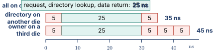
Two design conclusions follow and both are worth stating unprompted.
Placement of the home node becomes an architectural decision. In a monolithic design, which last-level-cache slice owns an address is a hashing decision made mostly for load balancing. Across dice it becomes a locality decision, because a home node on the wrong die costs a round trip on every access. That is the same reasoning as the address-mapping argument in DRAM Controllers JEDEC and DFI Part 5.2, transplanted.
Occupancy becomes the binding constraint. The number of outstanding coherent transactions you need in order to keep a link busy is the bandwidth-delay product. At 256 GB/s and 100 ns of round-trip latency:
Four hundred simultaneous transactions is a large tracker structure, and if you build 128 of them your link runs at a third of its rate no matter how good the PHY is. This is the single most common way a chiplet system underperforms its data sheet, and it is a structure-sizing question, which is exactly the kind of question you can answer from Arbiters FIFOs and CAMs.
7.3 Error handling, which is the genuinely hard part
An on-die wire has a bit error rate low enough that a coherence protocol simply does not model errors. A die-to-die link does not have that property. It runs at tens of gigatransfers per second through a solder joint that has been thermally cycled, and it will have errors.
So the link must detect and correct them, and the only practical mechanism at these rates is CRC plus retry. That creates three problems the protocol layer must never see.
Variable latency. A retried flit arrives late. A protocol that assumed a bounded latency now sees an outlier, and a timeout tuned for the good case fires spuriously. Timeouts on a die-to-die-connected coherence protocol must be sized for the retry-storm case, not the typical case.
Reordering. If retry is per-flit and the link keeps sending while waiting for a replay, flits arrive out of order. Coherence protocols are very sensitive to ordering within a message class. Delivering an invalidate-acknowledge before the invalidate it acknowledges will produce a state machine transition that no designer wrote. The adapter therefore either replays everything after the failure point, which is simple and wasteful, or reorders at the receiver, which requires buffering and sequence numbers.
Duplication, which is the subtle one. A replay resends a flit. If the acknowledgement for the original was lost rather than the flit itself, the receiver now gets it twice. In a data-streaming protocol a duplicate is a corruption of the byte stream, which is bad. In a coherence protocol a duplicate is far worse. A duplicated credit return inflates the credit count and eventually overflows a queue. A duplicated invalidate-acknowledge lets a directory believe an invalidation completed when one participant has not seen it. A duplicated ownership transfer creates two owners of one line and the machine's memory model silently stops holding.
So the adapter must deliver exactly once, and exactly-once delivery over a lossy channel is not free: it requires sequence numbers, a replay buffer sized to the round trip, and an acknowledgement protocol that distinguishes "I did not receive it" from "I received it and my acknowledgement was lost."
And then the case where the link cannot recover at all. A network drops a packet and a higher layer retransmits. A coherence protocol has no higher layer. A lost coherence message is a transaction that never completes, which is a hang, and a hang is the worst possible failure because it produces no information. So a die-to-die-connected coherent system needs, at minimum, poison propagation, marking data as known-bad so it travels to a consumer that can report it, and transaction timeouts that convert a hang into a machine-check exception with a recorded address. Designing those is a genuinely interesting problem and volunteering that you have thought about it is a strong signal.
7.4 Flow control and deadlock, transplanted
From Interconnect and AMBA Part 4, a coherence protocol deadlocks if a request channel can be blocked by a response channel that is itself waiting on a request. The standard fix is virtual channels: independent buffer pools per message class, so that a backlog in one class cannot stall another, with credits managed per class.
Across a die boundary those virtual channels must all share one set of physical lanes. That is fine in principle, and it is what virtual channels were invented for. It creates two new hazards.
Shared buffering re-creates the deadlock. If the adapter's replay buffer, or its receive buffer, is a single shared pool, then one class filling it blocks every class, and you have carefully built virtual channels and then defeated them one layer down. The buffering must be partitioned per class, or at minimum reserved per class, and this is a review item rather than something that shows up in simulation.
Retry interacts with credits. A flit carrying credit returns that is retried delays those credits. If the transmitter is blocked waiting for credits that are stuck behind a retry that is itself waiting for buffer space, you have a dependency cycle across the layer boundary. This is the class of bug that formal verification is genuinely good at and simulation is genuinely bad at, for exactly the reasons in Verification Methodology, and if you have written formal properties over ordered protocol behaviour this is a place to say so.
7.5 What you actually do about all of this
Four mitigations, in roughly the order a real design applies them.
Cut where the traffic is not. The single most effective thing is to partition so that the cut plane carries as little coherent traffic as possible. Cutting between a compute complex and its I/O is nearly free. Cutting through the middle of a shared cache is nearly fatal.
Filter aggressively at the boundary. A snoop filter at each die's edge that knows which lines could possibly be cached on the other side turns most cross-die snoops into local negative answers. This is the Cache Coherence Protocols Part 5.4 snoop-filter argument, and its value goes up enormously when the alternative costs a package crossing rather than a few cycles.
Accept non-uniformity and expose it. If a cross-die access costs 1.8 times a local one, that is a NUMA system whether or not you call it one, and the honest response is to make the topology visible to the operating system so that it can place threads and pages accordingly, rather than pretending it is uniform and letting the scheduler discover it the hard way.
Size the trackers for the bandwidth-delay product, per 7.2, because otherwise none of the above matters.
08.Part 8, what this means for an RTL designer
Everything so far has been architecture and economics. This part is the job, and it is where your record actually maps.
8.1 Link training is a state machine, and it is your kind of state machine
A die-to-die link does not work when you power it on, for exactly the reasons a DDR interface does not, from DRAM Controllers JEDEC and DFI Part 10.3. Process, voltage, temperature, package trace length, and bump-to-bump variation all shift timing by more than the bit period, so the link must measure itself.
The publicly described UCIe link state machine progresses through named states: RESET, then SBINIT where the sideband is initialised and repaired, then MBINIT where the mainband is initialised and repaired or degraded and the data rate is set to the lowest supported rate, then MBTRAIN where the operational speed is established and clock-to-data centring and per-lane deskew are performed in sub-states, then LINKINIT, then ACTIVE. There are low-power states L1 and L2, a PHYRETRAIN path for recalibration, and a TRAINERROR state which is described as a transitional state that returns the machine to RESET after a fatal or non-fatal event. Public material notes that the RESET state has a minimum residency, on the order of milliseconds, to let phase-locked loops settle.
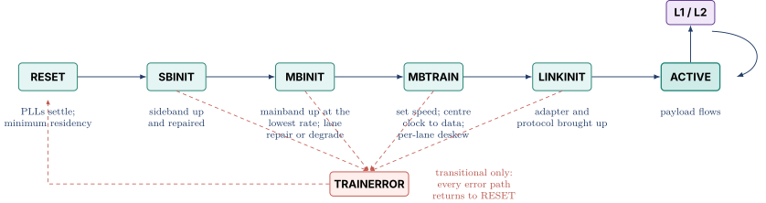
For an RTL designer this is a large, deeply nested, timed state machine with a partner state machine on another die that it can only talk to over a slow sideband, and every transition must be agreed by both sides. That is a hard piece of control logic, it is exactly the kind of thing formal verification is good at, and it is exactly the kind of thing you have written properties over. If you get one question about "what would you own on a die-to-die IP," this is the honest and strong answer.
Two properties worth naming as things you would prove rather than simulate: that the machine cannot reach ACTIVE unless both sides agreed the same configuration, and that every error path terminates in RESET rather than in a state with no exit. Liveness properties over a training sequence are precisely the class random simulation is worst at.
8.2 Lane repair, and the network you must not build
From 5.6, an advanced-package module has spare lanes and can repair failures. The interview question is how you implement that in RTL, and there is a right answer and a wrong one.
The wrong answer is a full crossbar: every logical lane able to source from any physical lane. For 32 lanes that is a 32-to-1 multiplexer replicated 32 times, which is enormous, slow, and sits directly in the highest-frequency path in the design.
The right answer exploits the structure of the problem. You are not remapping arbitrarily. You are skipping over failed lanes and shifting everything above by one position. So the network is a chain of 2-to-1 multiplexers. Logical lane takes physical lane or physical lane , depending on whether a failure has occurred at or below . One multiplexer deep, one gate of delay, and with two spares in a group you get two shift positions, which is a 3-to-1 select per lane at worst.
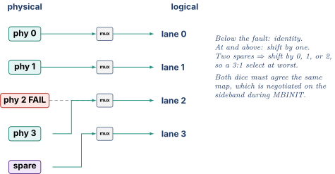
Three follow-ups worth having ready. How is the map decided? During MBINIT, by testing each lane and negotiating the repair configuration over the sideband. It must be agreed by both ends because a mismatched map silently scrambles the data. Where is the map stored? In registers that survive a retrain but must be re-established after a full reset, which means the training sequence has to run again, which means boot time. Can it be redone at runtime? Only through a retrain, which means the link goes down, which means the adapter must quiesce traffic first, which is the same quiesce-and-drain discipline as any power-state transition.
8.3 CRC and retry, and sizing the replay buffer
The mechanism is straightforward and the design content is entirely in the sizing and the corner cases.
Sizing. The replay buffer must hold every flit sent but not yet acknowledged, which is the bandwidth-delay product of the acknowledgement loop. At 256 GB/s with a 20 ns loop that is 5.12 kB per direction. Note what that means: the buffer is an SRAM, it is on the highest-bandwidth path in the design, it must be written every cycle and read on the replay path, and it grows linearly with both data rate and latency. Every generation that doubles the data rate doubles this SRAM. That is a real area and power cost that belongs in the pJ-per-bit accounting of Part 4.
Sequence numbers. Wide enough that the space exceeds the maximum in-flight count with margin, so a wrap cannot be mistaken for a fresh flit.
Acknowledgement. Piggybacked on reverse traffic where possible, with a standalone acknowledgement flit and a timer for the idle case, because a link with no reverse traffic must still drain its replay buffer.
The corner cases, which are where the bugs are. What happens if the acknowledgement itself is corrupted? If a retry request is corrupted? If both directions fail simultaneously? If the replay buffer fills while a retry is in progress? Each of those is an ordering question over a distributed pair of state machines, and each is a good formal property.
8.4 The clock domain crossing at the boundary
The receive path recovers data in the domain of the forwarded clock that came from the other die. The die's own logic runs on its own clock, generated by its own phase-locked loop from its own reference. Those two are asynchronous in the full sense of Clocking Reset and Domain Crossing: unrelated frequencies, unrelated phases, and drifting relative to each other.
So there is an asynchronous FIFO at the boundary with gray-coded pointers and the usual synchroniser discipline, and it is on the highest-bandwidth path in the design, which means it is wide and it is not cheap.
Then the hazard nobody mentions, and it is worth volunteering because it is the same structure you already know from two other notes. The forwarded clock stops in the low-power states. A synchroniser whose destination clock has stopped never resolves. So if the wake path for the link is itself synchronised into the forwarded-clock domain, the link cannot wake, because waking requires a clock that only starts once the link has woken. That is exactly the deadlock in Power Fundamentals and Clock Gating Part 4.4 and exactly the self-refresh deadlock in DRAM Controllers JEDEC and DFI Part 10.4, arriving for a third time in a new setting.
The resolution is the same one. The wake path must be on an always-running clock or must be asynchronous. In a die-to-die link there is a natural candidate, and it is the sideband, which is why the sideband is described as always-on and why it has its own forwarded clock separate from the mainband's. Being able to say "the sideband exists partly so that the mainband can be woken from a state in which the mainband's own clock is stopped" is a genuinely good observation and it comes free from material you already know.
8.5 Reset, power, and the fact that the other die can vanish
Two dice have separate power rails, separate reset trees, and separate clock generation. They can be powered and reset independently, and a robust design must assume they will be.
Reset domain crossing across a package. From Clocking Reset and Domain Crossing, a signal crossing between two reset domains can be sampled while its source is in reset and its destination is not, producing an undefined transition at the destination. Across a package this means that die A can be reset while die B is running, so every signal arriving at B from A must be either isolated or tolerant of A disappearing mid-transaction. B's link state machine has to detect the loss, abandon its outstanding transactions with an error rather than waiting forever, and return to RESET cleanly.
Isolation at the boundary. From Power Fundamentals and Clock Gating Part 7.3, an unpowered domain's outputs float toward mid-rail and a receiving gate in a powered domain sees an input between its thresholds, drawing crowbar current and producing an undefined output. Everything in that argument applies unchanged across a package, with one difference that makes it worse. On-die you can place an isolation cell in the powered domain and control it from an always-on domain. Across a package, the enable for that clamp has to come from somewhere that is still alive, and there is no shared always-on domain by construction. So the receiving die must clamp its own inputs based on its own knowledge of the link state, which means the link state machine is a safety mechanism and not only a bring-up mechanism.
Sequencing. Bringing up a two-die system is a distributed power-sequencing problem. Neither die can assume the other is ready. The sequence has to be negotiated, it has to have timeouts at every step, and it has to have a defined behaviour when a timeout fires. That is the same discipline as the power-down and power-up tables in Power Fundamentals and Clock Gating Part 7.4, and describing it in that vocabulary is one of the highest-value translations available to you in any of these interviews.
8.6 Test access across dice
Two distinct problems, and separating them is the mark of somebody who has thought about it.
Testing each die before assembly, which is the known-good-die problem from Part 2.3. Structurally this is ordinary scan and memory built-in self-test from DFT and Silicon Debug, with the additional constraint that it must run through a probe card at fine pitch, which limits parallelism and at-speed capability. The design response is to push more of the test on-die: more built-in self-test, more on-die compression so fewer probe pads are needed, and on-die measurement structures so the die can report its own timing margin rather than requiring an external measurement.
Testing the assembled stack, which is genuinely new. Once the dice are bonded you cannot probe the connections between them. They are microbumps or hybrid bonds under a die, physically inaccessible. So the interconnect itself must be testable from the outside through the dice, and there is a standard for the access architecture: IEEE Std 1838, approved at the end of 2019 and published in March 2020, defines a test access architecture for three-dimensional stacked integrated circuits. It is a die-centric standard, meaning it specifies what each die must provide so that any stack assembled from compliant dice is testable, rather than specifying a stack. Its publicly described components are four. A die wrapper register around each die lets that die and the interconnect above and below it be isolated and tested on its own. A primary test access port sits on the die that faces the outside world, with secondary test access ports on the dice above it. Serial test elevators carry stimulus up the stack and responses back down. And an optional flexible parallel port gives higher-bandwidth access than a serial port can. The purpose of all of it is modularity. Individual dice and the interconnect layers between adjacent dice can be tested separately rather than only as a whole.
For the die-to-die link specifically the practical mechanisms are loopback modes. Near-end loopback turns the transmitter back into the receiver on the same die to prove the PHY works without the package. Far-end loopback has the remote die return what it received to prove the channel works. Add an on-die pattern generator and checker so the link can run a bit-error-rate test on itself for as long as you like, and add per-lane error counters so a marginal lane is identifiable rather than showing up as an aggregate failure. All of that is design-for-test you must build in, because there is no way to add it afterwards, which is the DFT and Silicon Debug Part 8 argument arriving in a place where it is even more true than usual.
8.7 Where the bugs actually are
Worth having a list, because "what would you worry about" is a common question and a specific list beats a general answer.
The training sequence in its corner cases: an error at exactly the moment of a state transition, one side timing out while the other proceeds, a repair map agreed on one side and not the other.
The retry protocol in its corner cases: acknowledgement lost rather than data, both directions failing at once, replay buffer full during a retry.
The clock domain crossing when a clock stops, per 8.4.
The credit accounting when it interacts with retry, per 7.4, which is where a duplicated or lost credit turns into a slow leak that manifests as a hang after hours of running.
And the whole class of power and reset asymmetry bugs, where one die does something the other did not expect because they are genuinely independent machines.
Notice what those have in common. They are all distributed protocol ordering problems with enormous input-ordering spaces and small amounts of state, which is the formal verification sweet spot described in Verification Methodology Part 5.6. If you are asked how you would verify a die-to-die link, the structure of the answer is: assertions on the protocol rules, formal on the state machines and the credit and retry logic, simulation against a partner model for the data path, and a bit-error-rate loopback regression for the physical layer. Answering "UVM" and stopping is the failure mode.
09.Part 9, the interview questions, with answers
Fourteen questions of the kind actually asked when a role names chiplets, die-to-die interfaces, or advanced packaging, each with a model answer written the way a strong candidate would speak it rather than the way a textbook would write it, the follow-up the interviewer will reach for next, and the trap where there is one. Read them out loud. They are calibrated to be spoken in one to three minutes, which is the real constraint.
Q1. Why do chiplets exist?
Model answer. Three reasons, and they are in increasing order of how much money they actually save.
The first is yield, and I want to state it carefully because the usual version of it is wrong. Under a pure Poisson model, splitting a die into four and requiring all four to be good gives you exactly the same yield you started with, identically, because to the fourth power is . So "chiplets improve yield" is not by itself an argument. The real argument is silicon consumed per shipped product. With a defect density of 0.1 per square centimetre, an 800 square millimetre die yields about half, so you burn about 1600 square millimetres of silicon for every one you ship. Four 200 square millimetre dice yield about 82 percent each, so you burn about 970. Same function, 40 percent less silicon started. The point is not that defects got rarer, it is that each defect now throws away 200 square millimetres instead of 800.
The second reason is mixing process nodes, and it usually saves more. Logic scales well on a new node, SRAM scales much more slowly, and analogue and I/O barely scale at all. On a monolithic die you pay leading-node prices per square millimetre for a lot of area that gains nothing from being there. Split the I/O and analogue onto a mature node and, on the numbers I would work, the cost drops by more than half without shrinking anything.
The third is reuse. Four SKUs that differ only in compute capacity are four separate tapeouts monolithically and two die designs with chiplets. That halves the non-recurring engineering and it decouples the schedules, so the compute die can move to a new node without dragging the I/O die along.
The follow-up. "So why isn't everything a chiplet?"
Because there is a fixed packaging premium and a per-die test cost, and below some die size the silicon saving does not cover it. If I put the packaging premium at sixty dollars, the crossover on my numbers lands around 425 square millimetres, and it moves to roughly 310 at thirty dollars and roughly 590 at a hundred and twenty. So the honest answer is that the crossover is somewhere in the three-to-six hundred square millimetre region depending on the packaging premium, and that is why large server and accelerator parts went chiplet years before mobile parts did, and why mobile parts largely still have not.
The trap. Saying "better yield" and stopping. The interviewer will ask you to show it, and the naive version of the calculation says the gain is zero. Being the candidate who volunteers that the naive version is zero, and then explains where the gain actually is, is a completely different impression from being the candidate who has to be corrected.
Q2. When are chiplets the wrong answer?
Model answer. Four situations, and I would name them in this order.
When the die is small. Below the crossover the packaging premium dominates and you are simply paying more for a worse part.
When the cut plane carries a lot of latency-critical traffic. A crossing costs low single-digit nanoseconds each way in protocol pipeline, and the flight time is negligible so you cannot engineer it away. If the cut is between a core and its L2, that is fatal. If it is between a compute complex and its I/O, it is nearly free. The partition question is really a traffic question and I would want a traffic profile before choosing a cut.
When the power budget is tight. A terabyte per second across the package at half a picojoule per bit is four watts of pure interconnect. On a 300 watt part that is noise. On a 15 watt part it is more than a quarter of the budget and the product is dead. This is most of why phone-class SoCs stayed monolithic.
When the volume is low. The reuse argument amortises non-recurring engineering across SKUs and units. At low volume there is nothing to amortise across, and you have added packaging complexity and a new class of assembly yield risk for a saving that never arrives.
The follow-up. "What if the die is above the reticle limit?"
Then the question is different, because monolithic is not on the menu. A single die cannot exceed the stepper's reticle field, and the largest accelerators have been at that limit for years. At that point chiplets are not a cost optimisation, they are the only way to build the product at all, and the cost analysis is about how to partition rather than whether to.
The trap. Treating this as purely a cost question. Half the reasons above are technical, and an interviewer asking "when is it wrong" usually wants to hear the latency and power reasons, because those are the ones a designer has to live with.
Q3. Walk me through the packaging options and what each one buys.
Model answer. I would frame it as a ladder where every rung buys a finer connection pitch by putting something more expensive between the dice, because pitch is what sets everything else.
Bottom rung, an organic substrate with flip-chip bumps. Pitch is around 100 to 150 microns, set by what the build-up layers underneath can route out from under the bump field. It is cheap, mature, mechanically forgiving, and it will carry a signal tens of millimetres. It just cannot give you density.
Next, a silicon interposer, which is what 2.5D means. A large mostly-passive silicon die under everything, carrying damascene wiring at sub-micron line and space, with through-silicon vias bringing power up from the substrate. Microbump pitch drops to something like 40 to 55 microns and the wiring between dice becomes on-die quality. The complaint is that you are buying silicon area under the entire assembly including the regions where you only needed power.
Then embedded bridges, which answer that complaint directly. Put a small silicon bridge inside the substrate under just the seam between two dice. You get the interposer's local density where the connections actually are, you pay for silicon only there, power goes straight from substrate to die without a via trip, and there is no reticle ceiling on the package. The cost is a hard substrate manufacturing capability and a floorplan constraint, because the dense connections have to sit over the bridge.
Top rung, true 3D. Either thinned dice with through-silicon vias and microbumps in the tens of microns, or hybrid bonding, where two polished surfaces with recessed copper pads are bonded directly, copper to copper, with no solder at all. Hybrid bond pitch is publicly described as below ten microns and heading toward around one. Since density goes as the inverse square of pitch, going from a forty micron microbump to a four micron bond is a hundred times the connections per square millimetre, and the connection is a micron-scale copper stub with roughly a femtofarad of capacitance instead of a bump with tens.
The follow-up. "So why isn't everything hybrid bonded?"
Three reasons. Cost and process difficulty, since it needs atomic-scale flatness and a single particle ruins a large area. Thermal, because stacking puts one die's heat path through another and the die furthest from the sink runs hottest, which means you cannot stack two high-power dice. And known-good-die, because if the bonding is wafer to wafer you are bonding bad dice along with good ones and the composite yield is the product of the two wafers die by die, which destroys the economics from question one. Die-to-wafer bonding gets the known-good-die property back at the cost of throughput.
The trap. Saying 2.5D means "two and a half dimensions" as though it were a technical description. It is a joke that stuck. The content is that all the dice are coplanar but there is a silicon routing layer beneath them, and knowing that is the difference between having read the term and understanding it.
Q4. What is picojoules per bit and why is a die-to-die link so much better than a SerDes?
Model answer. It is total link energy divided by payload bits delivered, and the definition matters, because a number that counts only the output driver is not comparable to one that counts the clocking and the digital logic too. I would always ask what is included before comparing two numbers.
The reason a die-to-die link wins by an order of magnitude is not that the wire is shorter in some vague sense. It is that the reach changes what circuits the channel forces you to build, and there is a specific threshold.
Signals travel about six and a half picoseconds per millimetre in these materials. At thirty-two gigatransfers per second the bit period is about thirty-one picoseconds. So two millimetres of interposer is thirteen picoseconds of flight, which is under half a bit period, which means there is less than one bit on the wire at any instant and the wire behaves as a lumped capacitor. I can drive it with a plain inverter, unterminated, and pay . Twenty-five millimetres of substrate is a hundred and sixty picoseconds, which is five bit periods, so five bits are on the wire simultaneously, it is a transmission line, and I have to terminate it, and a terminated line burns static current.
A long-reach SerDes going across a board has tens of decibels of channel loss, so it needs a big driver, transmit equalisation, a continuous-time equaliser and a decision-feedback equaliser on the receive side, and a clock and data recovery loop. That is all continuous analogue and it is where the several picojoules per bit go. Delete the channel loss and you delete every one of those circuits, and you also get to forward the clock instead of recovering it, which removes both the loop and its latency.
The follow-up. "Put a number on the wire itself."
For the advanced-package case: two millimetres of interposer wiring at around 0.2 picofarads per millimetre is 0.4 picofarads, plus a bump and receiver, call it half a picofarad. Random data makes a zero-to-one transition once every four bits on average, so the energy is a quarter of , which at 0.75 volts is about 0.07 picojoules per bit. The published UCIe target for that package is about a quarter of a picojoule, so the wire is roughly a quarter of the budget and the transmitter, receiver, sampling clock, and digital logic are the other three quarters. That ratio is the design conclusion. At short reach, making the wire shorter buys almost nothing unless the PHY shrinks with it.
The trap. Attributing the whole advantage to capacitance. If it were only capacitance the ratio would track the length ratio, and it does not. The standard package is more than ten times the reach and only about twice the energy per bit, because the fixed PHY cost dominates at short reach. Getting that non-proportionality right is the tell.
Q5. Explain UCIe's layering. What lives where, and why is the boundary there?
Model answer. Three layers, and the interesting question is why the cuts are where they are rather than what they are called.
The physical layer is the analogue front end plus a logical PHY that runs link initialisation, training, calibration, and test and repair, plus a separate sideband channel used for parameter exchange and coordination with the partner die. This layer moves bits and deliberately knows nothing about what they mean.
The die-to-die adapter sits in the middle and does flit framing, CRC generation and checking, link-level retry, credit-based flow control, protocol multiplexing, and link power-state management.
The protocol layer hosts whatever is being carried, publicly PCIe, CXL, or a raw streaming mode for anything else.
The reason the adapter's boundary is where it is, is the whole architecture in one sentence. The protocol above was designed for an on-die fabric where wires do not corrupt data, so it has no concept of a lost or duplicated message. A die-to-die link at tens of gigatransfers through a thermally cycled solder joint definitely does have bit errors. So the adapter's entire job is to absorb that difference. It takes a channel that can lose bits and presents a channel that cannot, with no loss, no duplication, and order preserved. Everything in its responsibility list follows from that one requirement.
The other thing worth saying is what the standard is not. It is not a memory protocol, it is not a coherence protocol, and it is not a packaging technology. Nothing about it appears on a pin that leaves the package. It is an internal chip boundary, in the same way DFI is an internal boundary between a memory controller and its PHY.
The follow-up. "Why does the sideband exist when there is a high-speed link right next to it?"
Bootstrap. The mainband is not usable until it has been trained, and training requires the two dice to agree on data rate, lane mapping, and repair configuration. That negotiation has to happen over a channel that works with no configuration at all, so the sideband runs at a low fixed rate with its own forwarded clock. It is also the only channel you have in the lab when a link will not come up, and it is the natural place to put the wake path, because a synchroniser in the mainband's clock domain cannot resolve when that clock is stopped in a low-power state.
The trap. Describing it as a chiplet protocol in a way that implies it defines the transaction semantics. It defines a transport. If you want coherence across the package you still need a coherence protocol on top, and the publicly described example is Arm's CHI Chip-to-Chip riding on UCIe's streaming interface.
Q6. Standard package or advanced package? How do you choose?
Model answer. The choice is made for you by three things, and I would check them in order.
Distance. The advanced package mode is specified to a reach of about two millimetres, the standard mode to about twenty-five. If the two dice are not adjacent, the decision is already made.
Bandwidth needed per millimetre of shoreline. At roughly 110 micron pitch and 32 gigatransfers I get something like seventy gigabytes per second per millimetre of die edge. At 45 microns I get something like a hundred and eighty. If the product needs more than the standard package can deliver over the edge length I have available, I need the advanced package regardless of what it costs.
Energy budget. Roughly a quarter of a picojoule per bit versus roughly a half. At a terabyte per second that is a two-watt difference, which matters or does not depending on the part.
Then the thing that surprises people, which is that the two modes are not just faster and slower versions of the same design, they have different reliability strategies. The advanced package x64 module has spare lanes, publicly described as two groups of thirty-two data lanes with two spares each, so it repairs failures by remapping. The standard package x16 module has no spares at all, and instead degrades width, x16 to x8 to x4. The reason is bump economics. At 110 microns a spare bump costs real shoreline and is not worth it, and at 45 microns it is cheap. So a packaging parameter propagates all the way into a protocol feature, and that is worth knowing because it changes what my RTL has to implement.
The follow-up. "What has no repair path at all?"
The forwarded clock, the valid signal, the track signal, and the sideband. Public descriptions treat a failure in any of those as fatal for the module, and the recovery is to route traffic through other modules. That has a direct product consequence: module count is my redundancy granularity, so a design with a single module has no graceful degradation, and if field reliability matters I would want at least two even if one would carry the bandwidth.
The trap. Choosing on cost alone. Cost is the last of the four inputs, not the first, because the first three can eliminate a choice outright.
Q7. Design the lane repair logic.
Model answer. First I would say what I am not going to build, which is a crossbar. Letting any logical lane source from any physical lane is a thirty-two-to-one multiplexer replicated thirty-two times, sitting in the highest-frequency path in the design, and it will not close and it will not fit.
The structure of the problem is much kinder than that. I am not remapping arbitrarily, I am skipping over failed lanes. So logical lane either takes physical lane , or, if there has been a failure at or below , takes physical lane . That is a chain of two-to-one multiplexers, one gate deep. With two spares per group I need three positions, so a three-to-one select at worst, still one level.
The state is a small per-group register holding how many failures occurred below each position, or equivalently the shift amount. That is written once during training and read continuously, so it is a configuration register, not a datapath.
The part that actually needs care is not the multiplexer, it is the agreement. Both dice have to apply the same map, because if one shifts and the other does not, the data is silently scrambled and every downstream check fails in a way that does not point at the cause. So the map is negotiated over the sideband during mainband initialisation, both sides acknowledge it, and I would want an assertion and ideally a formal property that the link cannot reach the active state with mismatched maps.
The follow-up. "Can you repair at runtime?"
Not without a retrain, because changing the map mid-flight scrambles data in flight. So the sequence is: detect a rising per-lane error rate, quiesce the adapter so nothing is in flight, take the link down to retrain, re-run the repair negotiation, and come back up. That means runtime repair is a system-level event with a visible stall, not a transparent one, and it means the adapter needs a clean quiesce-and-drain capability. Which is the same requirement as entering a low-power state, so I would build one mechanism and use it for both.
The trap. Forgetting that repair has to be symmetric and negotiated. Candidates almost always design the multiplexer correctly and almost never mention that the other die has to be told, and the bug that creates is one of the nastiest kinds: functionally silent, data-dependent, and it looks like a physical layer problem when it is a control problem.
Q8. How does the link recover from a bit error, and what does that cost?
Model answer. CRC over each flit at the transmitter, checked at the receiver, and on a mismatch the receiver requests a replay and the transmitter resends from a replay buffer. That much is standard. The design content is in three places.
Sizing the replay buffer. It has to hold everything sent but not yet acknowledged, which is the bandwidth-delay product of the acknowledgement loop. At two hundred and fifty-six gigabytes per second with a twenty nanosecond loop that is about five kilobytes per direction. That is an SRAM on the highest-bandwidth path in the design, written every cycle, and it scales linearly with both the data rate and the latency, so every generation that doubles the rate doubles this memory. That cost belongs in the energy-per-bit accounting and people forget it.
Latency. Checking a CRC means waiting for the whole flit, so if I refuse to forward until the check passes I have added a full flit time of store-and-forward delay. At two hundred and fifty-six bytes and two hundred and fifty-six gigabytes per second that is a nanosecond. If instead I forward optimistically and cancel, I have pushed the problem to the consumer, which for a coherence protocol is usually unacceptable.
Exactly-once delivery, which is the part that matters most and gets mentioned least. If the data arrived fine and the acknowledgement was lost, the replay delivers a duplicate. For a byte stream a duplicate is corruption. For a coherence protocol it is much worse: a duplicated credit return inflates the credit count and eventually overflows a queue, a duplicated invalidate-acknowledge lets a directory think an invalidation completed when a participant never saw it, and a duplicated ownership transfer gives you two owners of a line and the memory model silently stops holding. So the adapter needs sequence numbers wide enough not to wrap into the in-flight window, and an acknowledgement protocol that distinguishes "not received" from "received, acknowledgement lost."
The follow-up. "What if it cannot recover?"
Then you cannot just drop it the way a network would, because a coherence protocol has no higher layer to retransmit and a lost coherence message is a transaction that never completes, which is a hang, and a hang gives you no information at all. So the design needs poison propagation, marking data as known-bad so it reaches a consumer that can report it, and transaction timeouts that convert a hang into a machine check with a recorded address. I would treat "this link can produce an unrecoverable error" as a first-class requirement rather than an afterthought, and I would want the timeout values and the error registers designed in from the start.
The trap. Describing CRC and retry as though it were the whole answer. Every candidate can describe retry. The distinguishing content is the buffer sizing, the store-and-forward latency, and the duplication hazard, and specifically the observation that duplication is far more dangerous in a coherence protocol than in a data stream.
Q9. Why is extending a cache coherence protocol across a die boundary hard?
Model answer. Because a coherence protocol makes five assumptions about its fabric and a package boundary breaks four of them.
It assumes messages are not lost, are not duplicated, are ordered within a class, that classes cannot block each other, and that latency is bounded. On-die all of that is free. Across a package, the link can corrupt bits, which means retry, which means variable latency and possible reordering and possible duplication, and it means the failure mode when recovery fails is a hang rather than a dropped packet.
The latency cost I would quantify rather than assert. If a local last-level-cache-and-directory transaction is twenty-five nanoseconds and a crossing costs about five each way, then a request to a directory on another die is thirty-five, and if the line is held modified on a third die it is forty-five. That is a factor of one point eight on exactly the accesses that occur when threads are sharing, which is exactly when software is already suffering, and it multiplies with any false-sharing penalty already present.
The occupancy cost is the one that actually breaks products. To keep a two-hundred-and-fifty-six gigabyte per second link busy at a hundred nanoseconds of round trip I need the bandwidth-delay product in flight, which is twenty-five kilobytes, which is four hundred cache lines, which is four hundred simultaneous outstanding transactions. If I build a hundred and twenty-eight trackers I get a third of my link bandwidth no matter how good the PHY is, and the data sheet will still say two hundred and fifty-six.
The flow control cost is that coherence needs independent virtual channels so that requests, snoops, responses, and data cannot block each other, and across the boundary they all share one physical link. That is fine in principle, but if the adapter's receive buffer or replay buffer is a single shared pool, one class filling it blocks all of them and I have rebuilt the deadlock the virtual channels existed to prevent, one layer down where nobody is looking.
The follow-up. "What would you do about the latency?"
Four things in order. Partition so the cut plane carries as little coherent traffic as possible, because a cut between compute and I/O is nearly free and a cut through a shared cache is nearly fatal. Put an aggressive snoop filter at each boundary so most cross-die snoops become local negative answers, which is worth far more here than on-die because the alternative costs a package crossing. Accept that it is a non-uniform memory system and expose the topology to software rather than pretending it is uniform. And size the trackers for the bandwidth-delay product, because none of the rest matters if the link is starved.
The trap. Answering only about latency. Latency is the obvious cost and it is not the hardest one. The hardest one is that a coherence protocol has no tolerance for duplication and no recovery path from a lost message, and that is what makes the adapter's exactly-once guarantee load-bearing.
Q10. How do you handle the clock domain crossing at the die boundary?
Model answer. The receive path lands in the domain of the clock that was forwarded from the other die. The local logic runs on a clock generated by the local phase-locked loop from a local reference. Those are asynchronous in the full sense: unrelated frequency, unrelated phase, drifting. So it is an asynchronous FIFO with gray-coded pointers and two-flop synchronisers on each pointer, and it is wide and on the highest-bandwidth path in the design so it is not a cheap structure.
Then the hazard that is easy to miss and that I would raise before being asked. The forwarded clock stops in the link's low-power states. A synchroniser whose destination clock has stopped never resolves. So if the wake path is synchronised into the forwarded-clock domain, the link cannot wake up, because waking requires a clock that only starts once the link has woken. That is a genuine deadlock and it is the same structure as gating a synchroniser's clock in a power-managed block, and the same structure as a memory controller whose clock stops during self-refresh.
The fix is the same one in all three cases. The wake path has to be on an always-running clock or be fully asynchronous. In a die-to-die link there is a natural candidate, because the sideband is described as always-on with its own forwarded clock separate from the mainband's. So one of the things the sideband exists for is to be able to wake a mainband whose own clock is stopped.
The follow-up. "What about the reset side?"
Same structural problem, different mechanism. The two dice have independent reset trees and either can be reset while the other runs, so every signal arriving from the other die has to be tolerant of the source disappearing mid-transaction. My link state machine has to detect the loss, terminate outstanding transactions with an error rather than waiting forever, and return cleanly to reset. And there is an isolation problem too. If the other die powers down, its outputs float toward mid-rail, and a receiving gate with a mid-rail input draws crowbar current and produces an undefined output that propagates. On-die I would put an isolation cell in the powered domain with its enable driven from an always-on domain. Across a package there is no shared always-on domain, so the receiving die has to clamp its own inputs based on its own view of the link state. That makes the link state machine a safety mechanism, not just a bring-up mechanism, which changes how carefully I would verify it.
The trap. Treating this as a routine asynchronous FIFO question. The FIFO is the easy half. The interesting half is what happens when the far clock stops or the far die disappears, and volunteering that unprompted is what distinguishes the answer.
Q11. How do you test a chiplet-based product, and what makes known-good die hard?
Model answer. Two separate problems and I would keep them separate because the techniques are different.
Before assembly. Each die has to be tested at wafer level, and this is where the economics from question one live, because if I assemble a bad die I have thrown away all the good ones plus the interposer plus the assembly. The difficulty is that wafer probe is genuinely weaker than packaged test, for physical reasons. Probe needles are comparable in size to the bumps at these pitches, so fine-pitch probing is slow and damaging and limits how many pads I can touch at once, which limits parallel test and therefore cost. Contact resistance through a probe is worse than a soldered joint, so at-speed I/O test is limited. Wafer-level thermal control is worse, so testing at the temperature corners where marginal parts fail is harder. And the die has not yet experienced the mechanical and thermal stress of assembly, which is exactly the stress that turns a marginal defect into a failure.
The design response is to move test on-die: more built-in self-test, more on-die compression so I need fewer probe pads, and on-die margin measurement so the die reports its own timing headroom rather than needing an external measurement.
After assembly. Now I cannot probe the connections at all, because they are microbumps or hybrid bonds under a die. So the interconnect has to be testable through the dice, and there is a standard for the access architecture, IEEE 1838, which is die-centric and defines a die wrapper register around each die, a primary test access port on the die facing the outside world with secondary ports on the dice above it, and serial test elevators carrying stimulus up the stack and responses back down, so individual dice and the layers between adjacent dice can be tested modularly.
For the link itself the practical mechanisms are loopback. Near-end loopback proves the PHY without the package. Far-end loopback proves the channel. Add an on-die pattern generator and checker and per-lane error counters so I can run a bit-error-rate test and identify a marginal lane rather than seeing an aggregate failure.
The follow-up. "What does escape rate at die test do to your product yield?"
It compounds. If each die is known-good with probability and I assemble of them, the probability the assembly is built entirely from good dice is before I count any assembly defects at all. At ninety-nine percent and eight dice that is already ninety-two percent. So test escape enters product cost raised to the chiplet count, which is a strong argument for spending on test and a real argument against very high chiplet counts. It also means the cost model in question one is sensitive to my test capability, not just to my defect density.
The trap. Treating it as ordinary DFT with more instances. The genuinely new content is that the interconnect between dice is physically inaccessible after assembly, so it has to be designed to test itself, and there is no way to add that afterwards.
Q12. You have a 700 square millimetre monolithic design. Partition it.
Model answer. I would ask two questions before drawing anything, and I would say so, because a partition proposed without them is guessing.
First, where is the traffic? I want a bandwidth and latency profile between every pair of major blocks. The cut plane should be a minimum cut of that graph weighted by latency sensitivity, not by bandwidth alone, because bulk bandwidth across a package is cheap and latency-critical coherent traffic is not.
Second, what does not want to be on the leading node? That is usually the largest single win, and it is usually obvious: SerDes, analogue, PHYs, pads, and anything driven by an external standard rather than by my own frequency target.
With those, the default shape I would start from is compute chiplets on the leading node and one or more I/O dice on a mature node. Concretely for seven hundred square millimetres, say two compute chiplets of about a hundred and seventy-five each on the leading node, and one I/O die of about three hundred and fifty on a mature node. That gets me the yield gain on the expensive silicon and the node-mixing gain on the cheap silicon, and the cut plane is compute-to-I/O, which is the cut that carries the least latency-critical traffic.
There are three cuts I would refuse without a very strong reason. Through a core, because pipeline stages cannot tolerate nanoseconds. Between a core and its private caches, same reason. And through the middle of a shared last-level cache, because that turns every cache access into a coin flip on whether it costs a package crossing.
Then the constraint people forget. The blocks that talk across the boundary have to sit near the die edge, because that is where the bumps are, and shoreline is scarce. So the partition is also a floorplan decision, and if the block that needs to talk across is architecturally in the middle of the die, either the partition or the floorplan has to change.
The follow-up. "What if you need a shared last-level cache across both compute dice?"
Then I would keep the cache with its home nodes on one die per address range and accept the non-uniformity, rather than trying to make it look uniform. I would put a snoop filter at each boundary so a cross-die snoop that will miss never crosses. I would make the address-to-home-node mapping a design parameter rather than a fixed hash, so that locality can be tuned against real traffic the way an address map is tuned in a memory controller. And I would size the outstanding transaction trackers for the bandwidth-delay product of the cross-die path, because that is the number that decides whether the link runs at its rated bandwidth.
The trap. Partitioning by block diagram tidiness. The natural-looking cut, one that follows the architectural hierarchy, is often exactly the wrong one, because architectural hierarchy reflects design-team boundaries rather than traffic. Saying "I would cut where the traffic is not, and I would need the traffic data to know where that is" is the correct opening and is not a dodge.
Q13. What breaks thermally and mechanically when you stack?
Model answer. Thermally, the problem is that heat leaves through the back of the die into the sink, and stacking puts one die in another die's heat path. The die furthest from the sink has the highest thermal resistance to it, and in a logic-on-logic stack the die in the middle can be hottest of all because it is heated from below and insulated from above. The thermal interface material and the bump layer are both poor conductors relative to silicon, so each interface adds resistance.
The architectural consequence is direct and it is the thing to say: you cannot stack two high-power dice. What works is high power on top of low power, which is why the publicly described 3D logic products put compute on a base die holding cache, I/O, and power delivery, rather than compute on compute. If I were partitioning for a stack, the first rule would be to put the power density where it can get out.
There is a second thermal effect worth naming. Leakage rises steeply with temperature, roughly doubling every ten degrees on the usual approximation, so a hotspot in a stack is a positive feedback loop in exactly the way it is in a monolithic part, only with worse thermal resistance to fight it with. So the thermal design point has to be conservative or the part throttles.
Mechanically, the driver is coefficient of thermal expansion mismatch. Silicon is around two and a half parts per million per kelvin, copper around seventeen, and an organic substrate is in the same region as copper in plane and considerably higher through its thickness. The mismatch that drives the failures is everything else against silicon. Every thermal cycle makes the layers try to grow by different amounts, and the stress concentrates at the small features: microbump joints, through-silicon via sidewalls, hybrid-bond interfaces, and underfill. The failure modes are warpage, voiding in vias, delamination, and cracking, and they are cumulative, which means they show up in reliability qualification rather than in first silicon.
The follow-up. "Does any of that affect the RTL or the timing?"
Yes, in a way that surprises people. Local mechanical stress changes carrier mobility, which changes drive strength, which changes delay. Stress around a through-silicon via is significant enough that physical design tools enforce a keep-out zone in which standard cells cannot be placed, so a via costs you area well beyond its own footprint. And the thermal gradients across a stacked die are larger than across a monolithic one, which widens the on-die variation that static timing has to cover, so timing signoff corners get worse. Neither of those changes what the RTL says, but both change what closes.
The trap. Answering only about heat. The mechanical half is a genuine and separate reliability problem, and the fact that it shows up as a qualification failure rather than a bring-up failure is what makes it dangerous.
Q14. Silicon comes back. The die-to-die link trains at 4 GT/s but fails at 32. Debug it.
Model answer. The signature is informative before I touch anything, because "works slow, fails fast" eliminates a lot.
It is almost certainly not a functional bug in the protocol logic, because that logic runs identically at both rates and a state machine that works at four gigatransfers works at thirty-two. It is also almost certainly not a lane mapping or repair problem, because a scrambled map fails at every rate. So the fault is in the timing-dependent part: the training that happens between the two rates, or the electrical margin at the higher rate.
My first hypothesis is the per-lane deskew and clock-to-data centring, because that is the step that exists only at the higher rates. At four gigatransfers the bit period is two hundred and fifty picoseconds and the natural skew between lanes is small compared to it, so an untrained or badly trained link still works. At thirty-two the bit period is thirty-one picoseconds and lane-to-lane skew from bump position and package trace length is comparable to it, so the link only works if centring succeeded. So I would read the trained delay values out over the sideband and look at the distribution. If they are all at a rail, or all at the reset default, training did not converge and I have a control bug rather than an electrical one.
Second hypothesis is electrical margin, which I would separate from the first by measuring rather than guessing. Run the built-in bit-error-rate test with a deliberately swept sampling point and build an eye contour per lane. If every lane has a small but non-zero eye, I have a systemic margin problem, which points at supply noise, at the reference clock's jitter, or at a package channel worse than modelled. If one or two lanes are bad and the rest are fine, that is a physical defect and it is exactly what the lane repair mechanism is for, and I should ask why repair did not engage.
Third, supply and clock. Ramping the link to full rate turns on a lot of switching at once, which is a di/dt event on a shared rail, and the resulting droop hits the receiver's own sampling clock. That would show as a failure that depends on how many lanes are active and on what the rest of the die is doing, which is a distinctive and testable signature.
So the plan is: read the trained values first because it is free, then run the built-in eye measurement per lane, then vary one thing at a time, rate, voltage, temperature, and active lane count, and see which one moves the failure.
The follow-up. "What would you have built in to make this debuggable?"
The sideband has to work at the lowest rate with no training, because it is my only channel when the mainband is dead, and I would not put anything on the critical debug path that depends on the mainband. Then: readable trained delay values and repair maps, per-lane error counters rather than an aggregate, a sweepable sampling point so the eye can be measured in situ, near-end and far-end loopback so I can separate the PHY from the channel, and a way to force the link to a specific rate and a specific repair configuration so I can bisect. All of that has to be designed in, and none of it can be added after tapeout, which is the general design-for-debug argument arriving in a place where the alternative is having no visibility at all.
The trap. Reaching for the protocol logic. Logic bugs do not usually care about the data rate. The rate dependence points at training and at electrical margin, and saying so first shows you reasoned from the evidence rather than from where you are most comfortable.
10.Part 11, check yourself
Answer out loud, in full sentences, as an interviewer would hear them. If you cannot, reread the section named.
- Show that splitting a die into four under a Poisson yield model changes the probability that all four are good by exactly nothing, then explain where the real economic gain comes from. (1.1, 1.2)
- Write the negative binomial yield model, explain what the clustering parameter does, and say why a large die's yield goes up when you account for clustering. (1.3)
- Work the silicon-consumed-per-shipped-product figure for an 800 mm² die and for four 200 mm² dice, under both yield models, and say why the conclusion is robust. (1.2, 1.3)
- Sketch the cost crossover between monolithic and four-way split, name the inputs it depends on, and say how far it moves when the packaging premium goes from thirty to a hundred and twenty dollars. (1.5)
- Explain the node-mixing argument and work an example. Why does it usually save more money than the yield argument? (1.6)
- Explain the reuse argument, and say what design constraint it imposes that architects dislike. (1.7)
- Name five costs of splitting a die and quantify at least two of them. (2.1 through 2.5)
- Why is the flight time across a package irrelevant, and what does the crossing latency actually consist of? (2.2)
- What is known-good die, why is wafer probe weaker than packaged test, and what does escape rate do to product yield as chiplet count rises? (2.3, Q11)
- Climb the packaging ladder from organic substrate to hybrid bonding, giving the approximate pitch and the thing you pay for at each rung. (3.1 through 3.6)
- Compute the flight time for 2 mm and 25 mm at a 32 GT/s bit period, and explain why that single calculation determines whether you may leave the line unterminated. (4.1)
- Derive shoreline bandwidth density from bump pitch for a 110 µm and a 45 µm pitch, and say which scaling exponent applies to shoreline density and which to areal density. (4.2)
- Derive an energy-per-bit floor for a 2 mm interposer link from , compare it to the published target, and say what the difference tells you about where to spend design effort. (4.3)
- Give UCIe's three layers, and explain why the adapter's boundary is where it is in terms of what the protocol layer must never see. (5.2)
- Why does the sideband exist? Give two independent reasons. (5.3, 8.4)
- Compare the standard-package and advanced-package modes on pitch, reach, module width, energy, and repair strategy, and explain why the repair strategies differ. (5.6)
- Name three other public die-to-die approaches and say what problem each solves. Why does HBM count as evidence? (6)
- List the five assumptions a coherence protocol makes about its fabric and say which ones a package boundary breaks. (7.1)
- Work the latency of a coherent transaction that stays on-die, crosses once, and crosses twice, and say what that does to the false-sharing penalty. (7.2)
- Why is duplication more dangerous than loss for a coherence protocol? Give three specific failures a duplicated message causes. (7.3)
- Compute the outstanding-transaction count needed to keep a 256 GB/s link busy at 100 ns of round trip, and say what happens if you build half that. (7.2)
- Walk the link training state sequence and say what each state establishes. What must be true before SBINIT completes? (8.1)
- Design the lane repair network. Why is it not a crossbar, and what is the part that has to be negotiated? (8.2)
- Size a replay buffer for 256 GB/s and a 20 ns acknowledgement loop, and say how that number scales generation over generation. (8.3)
- Explain the clock-domain-crossing deadlock at a die boundary, and name the two other notes where the same structure appears. (8.4)
- Why can a receiving die not use an ordinary isolation cell when its partner powers down, and what does it do instead? (8.5)
- What is IEEE 1838 for, and what are the two loopback modes you would build into a die-to-die PHY? (8.6)
- A link trains at 4 GT/s and fails at 32. Give your three hypotheses in order and say what you would read first. (Q14)
11.Part 12, related notes
- Cache Coherence Protocols for the protocol whose fabric assumptions Part 7 breaks, for the directory and snoop-filter material behind 7.5, and for the false-sharing arithmetic that the cross-die latency multiplies
- Interconnect and AMBA for virtual channels, deadlock avoidance, and credit-based flow control, all of which Part 5.4 and Part 7.4 move across a package boundary
- Power Fundamentals and Clock Gating for the derivation Part 4.3 reuses, for the isolation-cell argument Part 8.5 transplants, and for the power-sequencing discipline that a two-die bring-up is a harder version of
- Clocking Reset and Domain Crossing for the asynchronous FIFO at the receive boundary, for reset domain crossing between independently reset dice, and for the synchroniser-with-a-stopped-clock deadlock in 8.4
- Arbiters FIFOs and CAMs for the arbitration inside the adapter's protocol multiplexing and for the queue-sizing reasoning behind the replay buffer and the transaction tracker
- CXL and Coherent Memory Expansion for CXL, one of the two named protocols the UCIe protocol layer carries natively, and for the coherent-attach model that a retimer taking the link off-package is meant to serve
- System IP Debug Trace and RAS for poison propagation, machine-check reporting, and the transaction timeouts that Part 7.3 demands when a die-to-die link cannot recover
- SRAM Arrays and ECC for the coding theory behind the CRC in Part 8.3, and for the detection-versus-correction trade that decides why a die-to-die link retries rather than corrects
- DFT and Silicon Debug for scan, built-in self-test, and the designed-in observability argument that Part 8.6 depends on entirely
- Verification Methodology for where formal, assertions, and simulation each belong on the bug classes listed in Part 8.7
- SoC Integration and Interfaces for the integration contract around a hard macro, which is what a die-to-die PHY is, and for the high-speed-IO material that Part 4.1 contrasts against
- DRAM Controllers JEDEC and DFI for DFI as the other example of a standardised internal chip boundary, for the training-and-recalibration argument that Part 8.1 mirrors, and for the stopped-clock synchroniser deadlock arriving there first
- STA Synthesis and Physical Design for the shoreline and floorplan constraints of Part 2.5 and for the timing-corner consequences of the thermal gradients in Part 2.4
- Reliability Aging and Variation for the thermal-cycling and stress mechanisms behind Part 2.4, and for the variation vocabulary that the other meaning of "die-to-die" belongs to
- Cross Company Context and Behavioral for the cluster framework used in Part 10.1 and for the sourcing discipline that governs how to talk about any company's packaging choices
- RISC V ISA Privileged and Vector for the separate gap that three of the five companies in Part 10.1 also screen on
- Trends, Constraints, and Quantitative Principles for the vault's die-cost equation, the dies-per-wafer approximation, and the Bose-Einstein yield model that Part 1 uses throughout